December 1990
Order Number 271029-005
M80287
80-BIT HMOS
NUMERIC PROCESSOR EXTENSION
Military
Y
High Performance 80-Bit Internal
Architecture
Y
Implements Proposed IEEE Floating
Point Standard 754
Y
Expands M80286 10 Datatypes to
Include 32- 64- 80-Bit Floating Point
32- 64-Bit Integers and 18-Digit BCD
Operands
Y
Object Code Compatible with M8087
Y
Built-In Exception Handling
Y
Operates in Both Real and Protected
Mode M80286 Systems
Y
Available in a 40-Pin Cerdip Package
Y
Protected Mode Operation Completely
Conforms to the M80286 Memory
Management and Protection
Mechanisms
Y
Directly Extends M80286 10 Instruction
Set to Trigonometric Logarithmic
Exponential and Arithmetic Instructions
for All Datatypes
Y
8 x 80-Bit Individually Addressable
Numeric Register Stack
Y
6 8 10 MHz
Y
Military Temperature Range
b
55 C to
a
125 C (T
C
)
The Intel M80287 is a high performance numerics processor extension that extends the M80286 10 architec-
ture with floating point extended integer and BCD data types The M80286 20 computing system (M80286
and M80287) fully conforms to the proposed IEEE Floating Point Standard Using a numerics oriented archi-
tecture the M80287 adds over fifty mnemonics to the M80286 20 instruction set making the M80286 20 a
complete solution for high performance numeric processing The M80287 is implemented in N-channel deple-
tion load silicon gate technology (HMOS) and packaged in a 40-pin ceramic package The M80286 20 is
object code compatible with the M80286 20 and M8088 20 Intel's HMOS III process provides superior
radiation tolerance for applications with stringent radiation requirements
HMOS is a patented process of Intel Corporation
271029 � 1
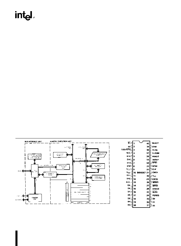
Figure 1 M80287 Block Diagram
271029 � 2
NOTE
N C pins must not be connected
Figure 2 M80287 Pin
Configuration

M80287
Table 1 M80287 Pin Description
Symbol
Type
Name and Function
CLK
I
CLOCK INPUT
This clock provides the basic timing for internal M80287
operations Special MOS level inputs are required The M82284 or M8284A
CLK outputs are compatible to this input
CKM
I
CLOCK MODE SIGNAL
Indicates whether CLK input is to be divided by 3
or used directly A HIGH input will select the latter option This input may be
connected to V
CC
or V
SS
as appropriate This input must be either HIGH or
LOW 20 CLK cycles before RESET goes LOW
RESET
I
SYSTEM RESET
Causes the M80287 to immediately terminate its present
activity and enter a dormant state RESET is required to be HIGH for more
than 4 M80287 CLK cycles For proper initialization the HIGH-LOW
transition must occur no sooner than 50 ms after V
CC
and CLK meet their
D C and A C specifications
D15 � D0
I O
DATA
16-bit bidirectional data bus Inputs to these pins may be applied
asynchronous to the M80287 clock
BUSY
O
BUSY STATUS
Asserted by the M80287 to indicate that it is currently
executing a command
ERROR
O
ERROR STATUS
Reflects the ES bit of the status word This signal
indicates that an unmasked error condition exists
PEREQ
O
PROCESSOR EXTENSION DATA CHANNEL OPERAND TRANSFER
REQUEST
A HIGH on this output indicates that the M80287 is ready to
transfer data PEREQ will be disabled upon assertion of PEACK or upon
actual data transfer whichever occurs first if no more transfers are required
PEACK
I
PROCESSOR EXTENSION DATA CHANNEL OPERAND TRANSFER
ACKNOWLEDGE
Acknowledges that the request signal (PEREQ) has been
recognized Will cause the request (PEREQ) to be withdrawn in case there
are no more transfers required PEACK may be asynchronous to the
M80287 clock
NPRD
I
NUMERIC PROCESSOR READ
Enables transfer of data from the M80287
This input may be asynchronous to the M80287 clock
NPWR
I
NUMERIC PROCESSOR WRITE
Enables transfer of data to the M80287
This input may be asynchronous to the M80287 clock
NPS1 NPS2
I
NUMERIC PROCESSOR SELECTS
Indicates the CPU is performing an
ESCAPE instruction Concurrent assertion of these signals (i e NPS1 is
LOW and NPS2 is HIGH) enables the M80287 to perform floating point
instructions No data transfers involving the M80287 will occur unless the
device is selected via these lines These inputs may be asynchronous to the
M80287 clock
CMD1 CMD0
I
COMMAND LINES
These along with select inputs allow the CPU to direct
the operation of the M80287 No actions will occur if these signals are both
HIGH These inputs may be asynchronous to the M80287 clock
CLK286
I
CPU CLOCK
This input provides a sampling edge for the M80287 inputs
S1 S0 COD INTA READY and HLDA It must be connected to the
M80286 CLK input
S1 S0
I
STATUS
These inputs allow the M80287 to monitor the execution of
COD INTA
ESCAPE instructions by the M80286 They must be connected to the
corresponding M80286 pins
HLDA
I
HOLD ACKNOWLEDGE
This input informs the M80287 when the M80286
controls the local bus It must be connected to the M80286 HLDA output
READY
I
READY
The end of a bus cycle is signaled by this input It must be
connected to the M80286 READY input
V
SS
I
GROUND
System ground both pins must be connected to ground
V
CC
I
POWER a
5V supply
2
M80287
FUNCTIONAL DESCRIPTION
The M80287 Numeric Processor Extension (NPX)
provides arithmetic instructions for a variety of nu-
meric data types in M80286 20 systems It also exe-
cutes numerous built-in transcendental functions
(e g tangent and log functions) The M80287 exe-
cutes instructions in parallel with an M80286 It ef-
fectively extends the register and instruction set of
an M80286 10 system for existing M80286 data
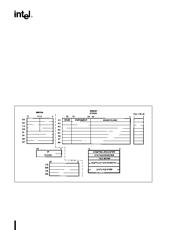
types and adds several new data types as well Fig-
ure 3 presents the program visible register model of
the M80286 20 Essentially the M80287 can be
treated as an additional resource or an extension to
the M80286 10 that can be used as a single unified
system the M80286 20
The M80287 has two operating modes similar to the
two modes of the M80286 when reset M80287 is in
the real address mode It can be placed in the pro-
tected virtual address mode by executing the
SETPM ESC instruction The M80287 cannot be
switched back to the real address mode except by
reset In the real address mode the M80286 20 is
completely software compatible with M8086 88 20
Once in protected mode all references to memory
for numerics data or status information obey the
M80286 memory management and protection rules
giving a fully protected extension of the M80286
CPU In the protected mode M80286 20 numerics
software
is
also
completely
compatible
with
M8086 20 and M8088 20
The M80287 has two operating modes similar to the
two modes of the M80286 When reset M80287 is
in the real address mode It can be placed in the
protected virtual address mode by executing the
SETPM ESC instruction The M80287 cannot be
switched back to the real address mode except by
reset
In
the
real
address
mode
the
M80286 M80287 is completely software compatible
with M8086 M8087 and M8088 M8087
Once in protected mode all references to memory
for numerics data or status information obey the
M80286 memory management and protection rules
giving a fully protected extension of the M80286
CPU In the protected mode M80286 M80287 nu-
merics software is also completely compatible with
M8086 M8087 and M8088 M8087
271029 � 3
Figure 3 M80286 20 Architecture
3

M80287
ABSOLUTE MAXIMUM RATINGS
Storage Temperature under Bias b65 C to a150 C
Case Temperature
b
55 C to a125 C
Voltage on any Pin with
Respect to Ground
b
1 0 to a7V
Power Dissipation
3 0 Watt
NOTICE This is a production data sheet The specifi-
cations are subject to change without notice
WARNING Stressing the device beyond the ``Absolute
Maximum Ratings'' may cause permanent damage
These are stress ratings only Operation beyond the
``Operating Conditions'' is not recommended and ex-
tended exposure beyond the ``Operating Conditions''
may affect device reliability
Operating Conditions
Symbol
Description
Min
Max
Units
T
C
Case Temperature (Instant On)
b
55
a
125
C
V
CC
Digital Supply Voltage
4 75
5 25
V
D C CHARACTERISTICS
(Over Specified Operating Conditions)
Symbol
Parameter
Min
Max
Unit
Test Conditions
V
IL
Input LOW Voltage
b
0 5
0 8
V
V
IH
Input HIGH Voltage
2 0
V
CC
a
0 5
V
V
ILC
Clock Input LOW Voltage
CKM e 1
2 0
V
CC
a
1
V
CKM e 0
3 8
V
CC
a
1
V
V
OL
Output LOW Voltage
0 45
V
I
OL
e
3 0 mA
V
OH
Output HIGH Voltage
2 4
V
I
OH
e b
400 mA
I
LI
Input Leakage Current
g
10
m
A
0V
s
V
IN
s
V
CC
I
LO
Output Leakage Current
g
10
m
A
0 45V
s
V
OUT
s
V
CC
I
CC
Power Supply Current
600
mA
T
C
e b
55 C
C
IN
Input Capacitance
10
pF
F
C
e
1 MHz
C
O
Input Output Capacitance
20
pF
F
C
e
1 MHz
(D0 � D15)
C
CLK
CLK Capacitance
12
pF
F
C
e
1 MHz
4

M80287
A C CHARACTERISTICS
(Over Specified Operating Conditions)
TIMING REQUIREMENTS
A C timings are referenced to 0 8V and 2 0V points on signals unless otherwise noted
Symbol
Parameter
6 MHz
8 MHz
10 MHz
Unit Comments
-6 Min -6 Max -8 Min -8 Max -10 Min -10 Max
T
CLCL
CLK Period
CKM e 1
165
500
125
500
100
500
ns
CKM e 0
62 5
166
50
166
40
166
ns
T
CLCH
CLK LOW Time
CKM e 1
100
343
68
343
53
343
ns At 0 8V
CKM e 0
15
146
15
146
11
146
ns At 0 6V
T
CHCL
CLK HIGH Time
CKM e 1
50
230
43
230
28
230
ns At 2 0V
CKM e 0
20
151
20
151
18
151
ns At 3 6V
T
CH1CH2
CLK Rise Time
10
10
10
ns 1 0V to 3 6V
if CKM e 1
T
CL2CL1
CLK Fall Time
10
10
10
ns 3 6V to 1 0V
if CKM e 1
T
DVWH
Data Setup to NPWR Inactive
75
75
75
ns
T
WHDX
Data Hold from NPWR Inactive
30
18
18
ns
T
WLWH
NPWR NPRD Active Time
95
90
90
ns At 0 8V
T
RLRH
T
AVRL
Command Valid to NPWR or
0
0
0
ns
T
AVWL
NPRD Active
T
MHRL
Minimum Delay from PEREQ
130
130
100
ns
Active to NPRD Active
T
KLKH
PEAK Active Time
85
85
60
ns At 0 8V
T
KHKL
PEAK Inactive Time
250
250
200
ns At 2 0V
T
KHCH
PEAK Inactive to NPWR
50
40
40
ns
NPRD Inactive
T
CHKL
NPWR NPRD Inactive to
b
30
b
30
b
30
ns
PEAK Inactive
T
WHAX
Command Hold from NPWR
30
30
22
ns
T
RHAX
NPRD Inactive
T
KLCL
PEAK Active Setup to NPWR
50
40
40
ns
NPRD Active
T
IVCL
NPWR NPRD RESET
70
70
53
ns
to CLK Setup Time
T
CLIH
NPWR NPRD RESET
45
45
37
ns
from CLK Hold Time
T
RSCL
RESET to CLK Setup Time
20
20
20
ns
T
CLRS
RESET from CLK Hold Time
20
20
20
ns
NOTE
T
ja
e
41 C W
T
jc
e
14 C W
5
M80287
A C CHARACTERISTICS
(Over Specified Operating Conditions)
TIMING RESPONSES
Symbol
Parameter
6 MHz
8 MHz
10 MHz
Unit Comments
-6 Min -6 Max -8 Min -8 Max -10 Min -10 Max
T
RHQZ
NPRD Inactive to Data Float
37 5
35
25
ns
(Note 2)
T
RLQV
NPRD Active to Data Valid
60
60
60
ns
(Note 3)
T
ILBH
ERROR Active to BUSY
100
100
100
ns
(Note 4)
Inactive
T
WLBV
NPWR Active to BUSY Active
100
100
100
ns
(Note 5)
T
KLML
PEACK Active to PEREQ
127
127
127
ns
(Note 6)
Inactive
T
CMDI
Command Inactive Time
Write-to-Write
95
95
75
ns
At 2 0V
Read-to-Read
95
95
75
ns
At 2 0V
Write-to-Read
95
95
75
ns
At 2 0V
Read-to-Write
95
95
75
ns
At 2 0V
T
RHCH
Data Hold from NPRD
3
3
3
ns
(Note 7)
Inactive
NOTES
2 Float condition occurs when output current is less than I
LO
on D0 � D15
3 D0 � D15 loading CL
e
100 pF
4 BUSY loading CL
e
100 pF
5 BUSY loading CL
e
100 pF
6 On last data transfer of numeric instruction
7 D0 � D15 loading CL
e
100 pF
6
M80287
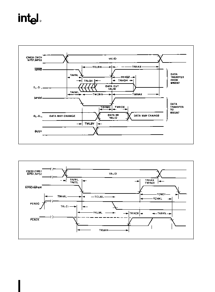
WAVEFORMS
DATA TRANSFER TIMING
(Initiated by M80286)
271029 � 16
DATA CHANNEL TIMING
(Initiated by M80287)
271029 � 17
7
M80287
WAVEFORMS
(Continued)
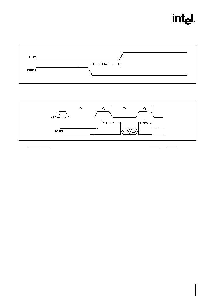
ERROR OUTPUT TIMING
271029 � 18
CLK RESET TIMING (CKM e 1)
271029 � 19
NOTE
Reset NPWR NPRD are inputs asynchronous to CLK Timing requirements for RESET NPWR and NPRD are given for
testing purposes only to assure recognition at a specific CLK edge
8

M80287
WAVEFORMS
(Continued)
CLK NPRD NPWR TIMING (CKM e 1)
271029 � 20
CLK RESET TIMING (CKM e 0)
271029 � 21
NOTE
Reset must meet timing shown to guarantee known phase of internal
d
3 circuit
CLK NPRD NPWR TIMING (CKM e 0)
271029 � 22
NOTE
Reset NPWR NPRD are inputs asynchronous to CLK Timing requirements for RESET NPWR and NPRD are given for
testing purposes only to assure recognition at a specific CLK edge
9
M80287
WAVEFORMS
(Continued)
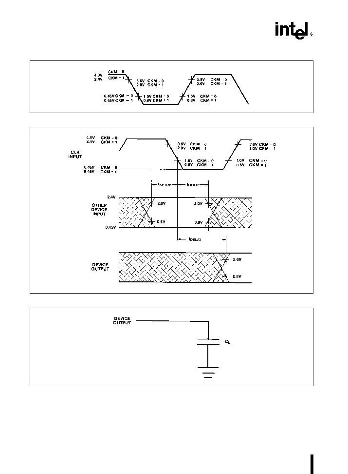
271029 � 23
AC Drive and Measurement Points
CLK Input
271029 � 24
AC Setup Hold and Delay Time Measurement
General
271029 � 25
AC Test Loading on Outputs
10

M80287
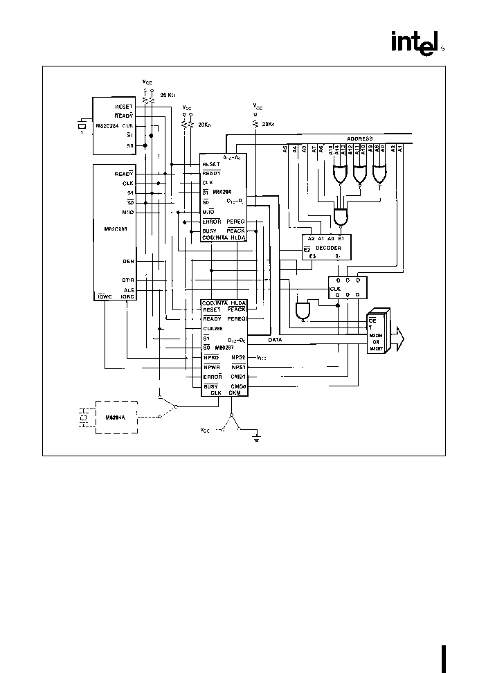
SYSTEM CONFIGURATION WITH
M80286
As a processor extension to an M80286
the
M80287 can be connected to the CPU as shown in
Figure 4 The data channel control signals (PEREQ
PEACK) the BUSY signal and the NPRD NPWR
signals allow the NPX to receive instructions and
data from the CPU When in the protected mode all
information received by the NPX is validated by the
M80286 memory management and protection unit
Once started the M80287 can process in parallel
with and independent of the host CPU When the
NPX detects an error or exception it will indicate this
to the CPU by asserting the ERROR signal
The NPX uses the processor extension request and
acknowledge pins of the M80286 CPU to implement
data transfers with memory under the protection
model of the CPU The full virtual and physical ad-
dress space of the M80286 is available Data for the
M80287 in memory is addressed and represented in
the same manner as for an M8087
The M80287 can operate either directly from the
CPU clock or with a dedicated clock For operation
with the CPU clock (CKM e 0) the M80287 works
at one-third the frequency of the system clock (i e
for an 8 MHz M80286 the 16 MHz system clock is
divided down to 5 3 MHz) The M80287 provides a
capability to internally divide the CPU clock by three
to produce the required internal clock (33% duty cy-
cle) To use a higher performance M80287 (8 MHz)
an M8284A clock driver and appropriate crystal may
be used to directly drive the M80287 with a
duty
cycle clock on the CLK input (CKM e 1)
SYSTEM CONFIGURATION WITH
M80386
The M80287 can also be connected as a processor
extension to the M80386 CPU as shown in Figure
4b
All software written for M8086 M8087 and
M80286 M80287 is object code compatible with
80386 M80287 and can benefit from the increased
speed of the M80386 CPU
Note that the PEACK input pin is pulled high This is
because the M80287 is not required to keep track of
the number of words transferred during an operand
transfer when it is connected to the M80386 CPU
Unlike the M80286 CPU the M80386 CPU knows
the exact length of the operand being transferred
to from the M80287 After an ESC instruction has
been sent to the M80287 the M80386 processor
extension data channel will initiate the data transfer
as soon as it receives the PEREQ signal from the
M80287 The transfer is automatically terminated by
the M80386 CPU as soon as all the words of the
operand have been transferred
Because of the very high speed local bus of the
M80386 CPU the M80287 cannot reside directly on
the CPU local bus A local bus controller logic is
used to generate the necessary read and write cycle
timing as well as the chip select timings for the
M80287 The M80386 CPU uses I O addresses
800000F8 through 800000FF to communicate with
the M80287 This is beyond the normal I O address
space of the CPU and makes it easier to generate
the chip select signals using A31 and M IO It may
also be noted that the M80386 CPU automatically
generates 16-bit bus cycles whenever it communi-
cates with the M80287
HARDWARE INTERFACE
Communication of instructions and data operands
between the M80286 and M80287 is handled by the
CMD0 CMD1 NPS1 NPS2 NPRD and NPWR sig-
nals I O port addresses 00F8H 00FAH and 00FCH
are used by the M80286 for this communication
When any of these addresses are used the NPS1
input must be LOW and NPS2 input HIGH The
IORC and IOWC outputs of the M82288 identify I O
space transfers (see Figure 4) CMD0 should be
connected to latched M80286 A1 and CMD1 should
be connected to latched M80286 A2
I O ports 00F8H to 00FFH are reserved for the
M80286 M80287 interface To guarantee correct
operation of the M80287 programs must not per-
form any I O operations to these ports
The PEREQ PEACK BUSY and ERROR signals of
the M80287 are connected to the same-named
M80286 input The data pins of the M80287 should
be directly connected to the M80286 data bus Note
that all bus drivers connected to the M80286 local
bus must be inhibited when the M80286 reads from
the M80287 The use of COD INTA and M IO in the
decoder prevents INTA bus cycles from disabling
the data transceivers
The S1 S0 COD INTA READY HLDA and CLK
pins of the M80286 are connected to the same
named pins on the M80287 These signals allow the
M80287 to monitor the execution of ESCAPE in-
structions by the M80826
PROGRAMMING INTERFACE
Table 2 lists the seven data types the M80287 sup-
ports and presents the format for each type These
values are stored in memory with the least signifi-
cant digits at the lowest memory address Programs
retrieve these values by generating the lowest ad-
dress All values should start at even addresses for
maximum system performance
11
M80287
271029 � 4
Figure 4 M80286 20 System Configuration
Internally the M80287 holds all numbers in the tem-
porary real format Load instructions automatically
convert operands represented in memory as 16-
32- or 64-bit integers 32- or 64-bit floating point
numbers or 18-digit packed BCD numbers into tem-
porary real format Store instructions perform the re-
verse type conversion
M80287 computations use the processor's register
stack These eight 80-bit registers provide the equiv-
alent capacity of 40 16-bit registers The M80287
register set can be accessed as a stack with in-
structions operating on the top one or two stack ele-
ments or as a fixed register set with instructions
operating on explicitly designated registers
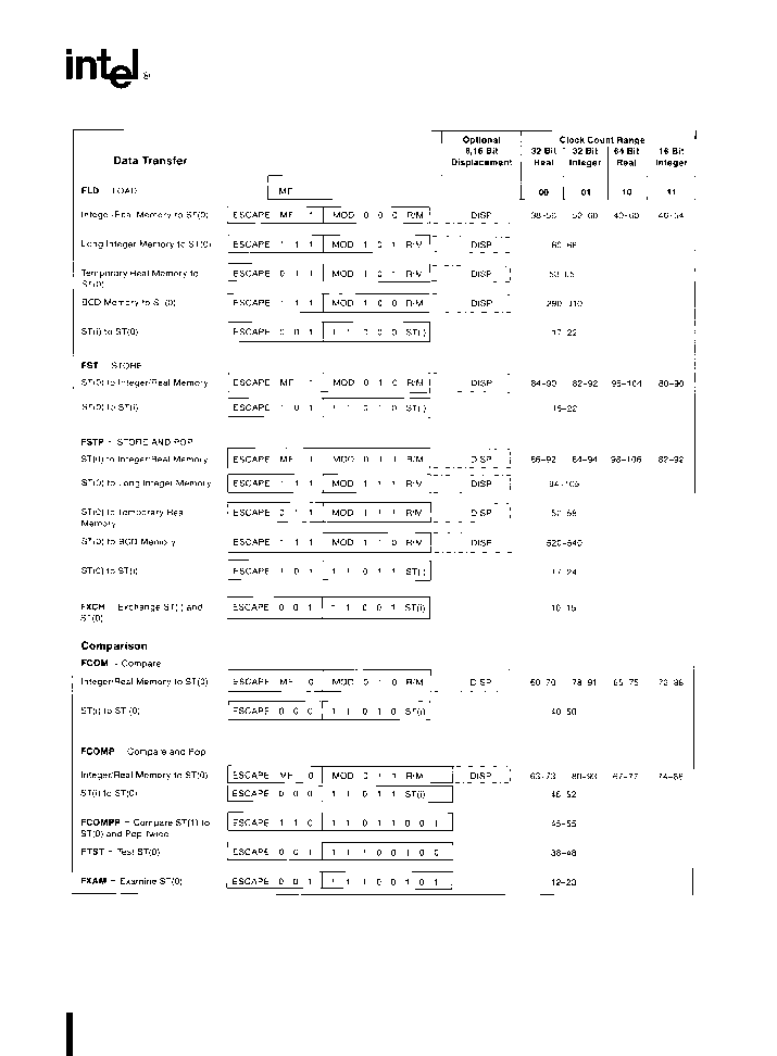
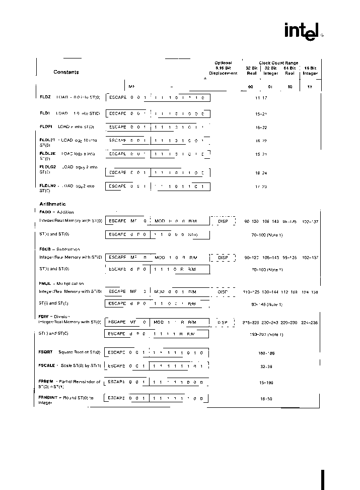
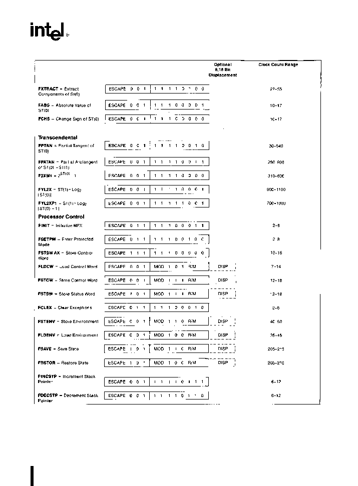
Table 6 lists the M80287's instructions by class No
special programming tools are necessary to use the
M80287 since all new instructions and data types
are directly supported by the M80286 assembler and
appropriate high level languages All M8086 88 de-
velopment tools which support the M8087 can also
be used to develop software for the M80286 in real
address mode
Table 3 gives the execution times of some typical
numeric instructions
12

M80287
Table 2 M80287 Datatype Representation in Memory
271029 � 5
NOTES
1 S
e
Sign bit (0
e
positive 1
e
negative)
2 d
n
e
Decimal digit (two per byte)
3 X
e
Bits have no significance M8087 ignores when loading zeros when storing
4
U
e
Position of implicit binary point
5 I
e
Integer bit of significand stored in temporary real implicit in short and long real
6 Exponent Bias (normalized values)
Short Real 127 (7FH)
Long Real 1023 (3FFH)
Temporary Real 16383 (3FFFH)
7 Packed BCD (
b
1)
S
(D
17
D
0
)
8 Real (
b
1)
S
(2
E-BIAS
) (F
0
F
1
)
SOFTWARE INTERFACE
The M80286 20 is programmed as a single proces-
sor All communication between the M80286 and
the M80287 is transparent to software The CPU au-
tomatically controls the M80287 whenever a numer-
ic instruction is executed All memory addressing
modes physical memory and virtual memory of the
CPU are available for use by the NPX
Since the NPX operates in parallel with the CPU any
errors detected by the NPX may be reported after
the CPU has executed the ESCAPE instruction
which caused it To allow identification of the failing
numeric instruction the NPX contains two pointer
registers which identify the address of the failing nu-
meric instruction and the numeric memory operand if
appropriate for the instruction encountering this er-
ror
13

M80287
Table 3 Execution Time for Selected M80287 Instructions
Approximate Execution
Floating Point Instruction
Time (ms)
M80287
(5 MHz Operation)
Add Subtract
14 18
Multiply (Single Precision)
19
Multiply (Extended Precision)
27
Divide
39
Compare
9
Load (Double Precision)
10
Store (Double Precision)
21
Square Root
36
Tangent
90
Exponentiation
100
INTERRUPT DESCRIPTION
Several interrupts of the M80286 are used to report
exceptional conditions while executing numeric pro-
grams in either real or protected mode The inter-
rupts and their functions are shown in Table 4
PROCESSOR ARCHITECTURE
As shown in Figure 1 the NPX is internally divided
into two processing elements the bus interface unit
(BIU) and the numeric execution unit (NEU) The
NEU executes all numeric instructions while the BIU
receives and decodes instructions requests oper-
and transfers to and from memory and executes
processor control instructions The two units are
able to operate independently of one another allow-
ing the BIU to maintain asynchronous communica-
tion with the CPU while the NEU is busy processing
a numeric instruction
BUS INTERFACE UNIT
The BIU decodes the ESC instruction executed by
the CPU If the ESC code defines a math instruction
the BIU transmits the formatted instruction to the
NEU If the ESC code defines an administrative in-
struction the BIU executes it independently of the
NEU The parallel operation of the NPX with the
CPU is normally transparent to the user The BIU
generates the BUSY and ERROR signals for
M80286 M80287 processor synchronization
and
error notification respectively
The M80287 executes a single numeric instruction
at a time When executing most ESC instructions
the M80286 tests the BUSY pin and waits until the
M80287 indicates that it is not busy before initiating
the command Once initiated the M80286 continues
program execution while the M80287 executes the
ESC instruction In M8086 20 systems this synchro-
nization is achieved by placing a WAIT instruction
before an ESC instruction For most ESC instruc-
tions the M80286 20 does not require a WAIT in-
struction before the ESC opcode However the
M80286 20 will operate correctly with these WAIT
instructions In all cases a WAIT or ESC instruction
should be inserted after any M80287 store to memo-
ry (except FSTSW and FSTCW) or load from memo-
ry (except FLDENV or FRSTOR) before the M80286
reads or changes the value
Data transfers between memory and the M80287
when needed
are controlled by the PEREQ
PEACK NPRD NPWR NPS1 NPS2 signals The
M80286 does the actual data transfer with memory
through its processor extension data channel Nu-
meric data transfers with memory performed by the
M80286 use the same timing as any other bus cycle
Control signals for the M80287 are generated by the
M80286 as shown in Figure 4 and meet the timing
requirements shown in the AC requirements section
14

M80287
Table 4 Interrupt Vectors
Interrupt Number
Interrupt Function
7
An ESC instruction was encountered when EM or TS of the M80286 MSW was
set EM e 1 indicates that software emulation of the instruction is required When
TS is set either an ESC or WAIT instruction will cause interrupt 7 This indicates
that the current NPX context may not belong to the current task
9
The second or subsequent words of a numeric operand in memory exceeded a
segment's limit This interrupt occurs after executing an ESC instruction The
saved return address will not point at the numeric instruction causing this interrupt
After processing the addressing error the M80286 program can be restarted at
the return address with IRET The address of the failing numeric instruction and
numeric operand are saved in the M80287 An interrupt handler for this interrupt
must
execute FNINIT before
any
other ESC or WAIT instruction
13
The starting address of a numeric operand is not in the segment's limit The return
address will point at the ESC instruction (including prefixes) causing this error The
M80287 has not executed this instruction The instruction and data address in
M80287 refer to a previous correctly executed instruction
16
The previous numeric instruction caused an unmasked numeric error The
address of the faulty numeric instruction or numeric data operand is stored in the
M80287 Only ESC or WAIT instructions can cause this interrupt The M80286
return address will point at a WAIT or ESC instruction including prefixes which
may be restarted after clearing the error condition in the NPX
NUMERIC EXECUTION UNIT
The NEU executes all instructions that involve the
register stack these include arithmetic logical tran-
scendental constant and data transfer instructions
The data path in the NEU is 84 bits wide (68 fraction
bits 15 exponent bits and a sign bit) which allows
internal operand transfers to be performed at very
high speeds
When the NEU begins executing an instruction it
activates the BIU BUSY signal This signal is used in
conjunction with the CPU WAIT instruction or auto-
matically with most of the ESC instructions to syn-
chronize both processors
REGISTER SET
The M80287 register set is shown in Figure 5 Each
of the eight data registers in the M8087's register
stack is 80 bits wide and is divided into ``fields'' cor-
responding to the NPX's temporary real data type
At a given point in time the TOP field in the status
word identifies the current top-of-stack register A
``push'' operation decrements TOP by 1 and loads a
value into the new top register A ``pop'' operation
stores the value from the current top register and
then increments TOP by 1 Like M80286 stacks in
memory the M80287 register stack grows ``down''
toward lower-addressed registers
Instructions may address the data registers either
implicitly or explicitly Many instructions operate on
the register at the top of the stack These instruc-
tions implicitly address the register pointed by the
TOP Other instructions allow the programmer to ex-
plicitly specify the register which is to be used Ex-
plicit register addressing is ``top-relative ''
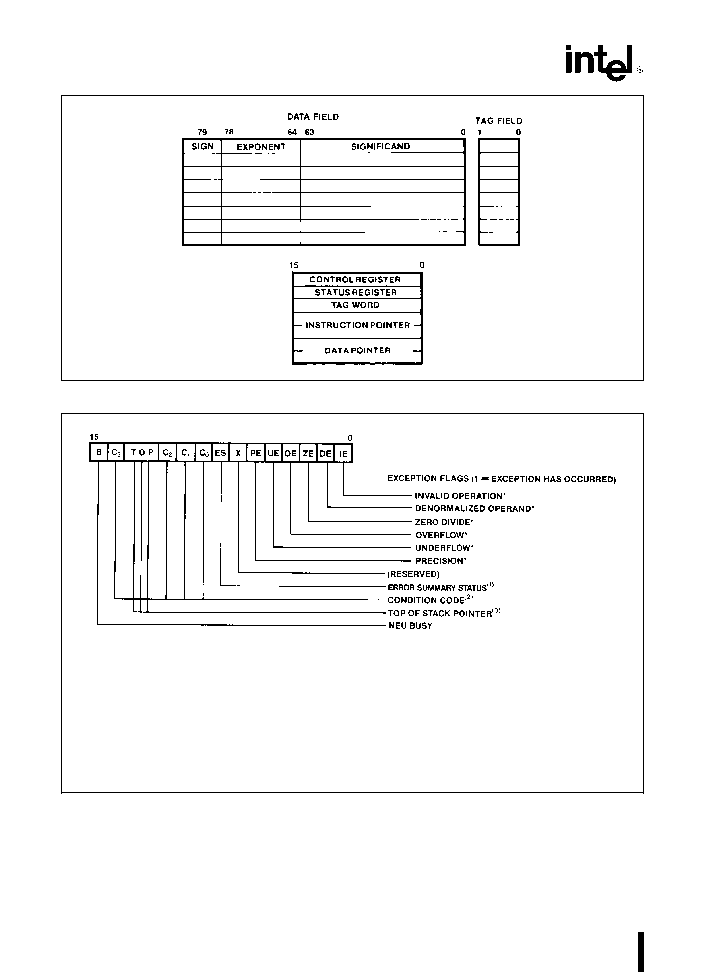
Status Word
The 16-bit status word (in the status register) shown
in Figure 6 reflects the overall state of the M80287
It may be read and inspected by CPU code The
busy bit (bit 15) indicates whether the NEU is exe-
cuting an instruction (B e 1) or is idle (B e 0)
The instructions FSTSW FSTENV FSTSWAX and
FSAVE which store the status word are executed
exclusively by the BIU and do not set the busy bit
themselves or require the Busy bit be cleared in or-
der to be executed
The four numeric condition code bits (C
0
� C
3
) are
similar to the flags in a CPU instructions that per-
form arithmetic operations update these bits to re-
flect the outcome of NDP operations The effect of
these instructions on the condition code bits is sum-
marized in Tables 5a and 5b
15
M80287
271029 � 11
Figure 5 M80287 Register Set
271029 � 6
NOTES
1 ES is set if any unmasked exception bit is set cleared otherwise
2 See Table 5 for condition code interpretation
3 Top Values
000
e
Register 0 is Top of Stack
001
e
Register 1 is Top of Stack
111
e
Register 7 is Top of Stack
For definitions see the section on exception handling
Figure 6 M80287 Status Word
16

M80287
Bits 14 � 12 of the status word point to the M80287
register that is the current top-of-stack (TOP) as de-
scribed above Figure 6 shows the six error flags in
bits 5 � 0 of the status word Bits 5 � 0 are set to indi-
cate that the NEU has detected an exception while
executing an instruction The section on exception
handling explains how they are set and used
Bit 7 is the error status bit This bit is set if any un-
masked exception bit is set and cleared otherwise If
this bit is set the ERROR signal is asserted
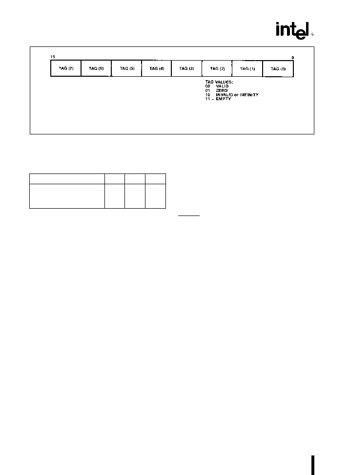
Tag Word
The tag word marks the content of each register as
shown in Figure 7 The principal function of the tag
word is to optimize the NPX's performance The tag
word can be used however to interpret the con-
tents of M80287 registers
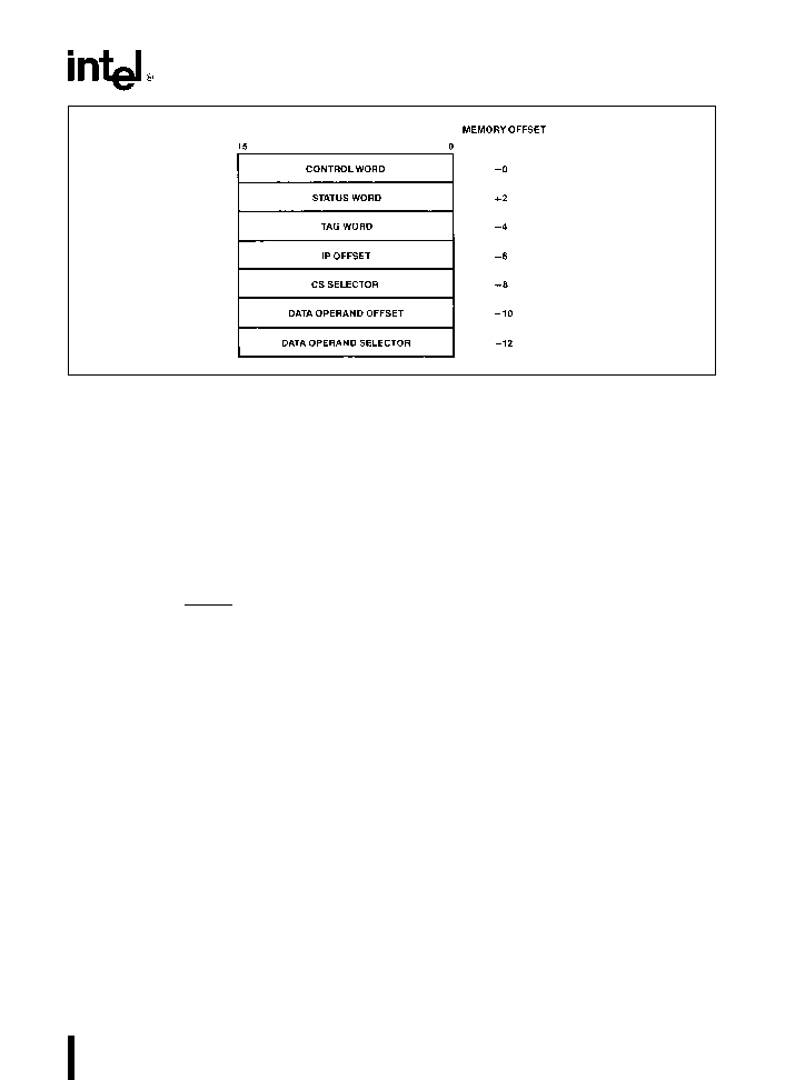
Instruction and Data Pointers
The instruction and data pointers (see Figures 8a
and 8b) are provided for user-written error handlers
Whenever the M80287 executes a new instruction
the BIU saves the instruction address the operand
address (if present) and the instruction opcode
M80287 instructions can store this data into memo-
ry
The instruction and data pointers appear in one of
two formats depending on the operating mode of the
M80287 In real mode these values are the 20-bit
physical address and 11-bit opcode formatted like
the M8087 In protected mode these values are the
32-bit virtual addresses used by the program which
executed an ESC instruction The same FLDENV
FSTENV FSAVE FRSTOR instructions as those of
the M8087 are used to transfer these values be-
tween the M80287 registers and memory
Table 5a Condition Code Interpretation
Instruction
C
3
C
2
C
1
C
0
Interpretation
Type
Compare Test
0
0
X
0
ST
l
Source or 0 (FTST)
0
0
X
1
ST
k
Source or 0 (FTST)
1
0
X
0
ST e Source or 0 (FTST)
1
1
X
1
ST is not comparable
Remainder
Q
1
0
Q
0
Q
2
Complete reduction with
three low bits of quotient
(See Table 5b)
U
1
U
U
Incomplete Reduction
Examine
0
0
0
0
Valid positive unnormalized
0
0
0
1
Invalid positive exponent e 0
0
0
1
0
Valid negative unnormalized
0
0
1
1
Invalid negative exponent e 0
0
1
0
0
Valid positive normalized
0
1
0
1
Infinity positive
0
1
1
0
Valid negative normalized
0
1
1
1
Infinity negative
1
0
0
0
Zero positive
1
0
0
1
Empty
1
0
1
0
Zero negative
1
0
1
1
Empty
1
1
0
0
Invalid positive exponent e 0
1
1
0
1
Empty
1
1
1
0
Invalid negative exponent e 0
1
1
1
1
Empty
NOTES
1 ST
e
Top of stack
2 X
e
value is not affected by instruction
3 U
e
value is undefined following instruction
4 Q
n
e
Quotient bit n
17
M80287
271029 � 12
NOTE
The index i of tag(i) is
not top-relative A program typically uses the ``top'' field of Status Word to determine which tag(i)
field refers to logical top of stack
Figure 7 M80287 Tag Word
Table 5b Condition Code Interpretation After
FPREM Instruction As a Function of
Dividend Value
Dividend Range
Q
2
Q
1
Q
0
Dividend
k
2
Modulus
C
3
C
1
Q
0
Dividend
k
4
Modulus
C
3
Q
1
Q
0
Dividend
t
4
Modulus
Q
2
Q
1
Q
0
NOTE
1 Previous value of indicated bit not affected by FPREM
instruction execution
The saved instruction address in the M80287 will
point at any prefixes which preceded the instruction
This is different than in the M8087 which only point-
ed at the ESCAPE instruction opcode
Control Word
The NPX provides several processing options which
are selected by loading a word from memory into the
control word Figure 9 shows the format and encod-
ing of fields in the control word
The low order byte of this control word configures
the M80287 error and exception masking Bits 5 � 0
of the control word contain individual masks for each
of the six exceptions that the M80287 recognizes
The high order byte of the control word configures
the M80287 operating mode including precision
rounding and infinity control The precision control
bits (bits 9 � 8) can be used to set the M80287 inter-
nal operating precision at less than the default of
temporary real (80-bit) precision This can be useful
in providing compatibility with the early generation
arithmetic processors of smaller precision than the
M80287 The rounding control bits (bits 11 � 10) pro-
vide for directed rounding and true chop as well as
the unbiased round to nearest even mode specified
in the IEEE standard Control over closure of the
number space at infinity is also provided (either af-
fine closure
g
%
or projective closure % is treat-
ed as unsigned may be specified)
EXCEPTION HANDLING
The M80287 detects six different exception condi-
tions that can occur during instruction execution
Any or all exceptions will cause the assertion of
ERROR signal if the appropriate exception masks
are not set
The exceptions that the M80287 detects and the
`default' procedures that will be carried out if the ex-
ception is masked are as follows
Invalid Operation
Stack overflow stack underflow
indeterminate form (0 0 % � % etc ) or the use of a
Non-Number (NAN) as an operand An exponent
value of all ones and non-zero significand is re-
served to identify NANs If this exception is masked
the M80287 default response is to generate a spe-
cific NAN called INDEFINITE or to propagate al-
ready existing NANs as the calculation result
Overflow
The result is too large in magnitude to fit
the specified format The M80287 will generate an
encoding for infinity if this exception is masked
Zero Divisor
The divisor is zero while the dividend
is a non-infinite
non-zero number
Again
the
M80287 will generate an encoding for infinity if this
exception is masked
Underflow
The result is non-zero but too small in
magnitude to fit in the specified format If this excep-
tion is masked the M82087 will denormalize (shift
right) the fraction until the exponent is in range The
process is called gradual underflow
18
M80287
271029 � 13
Figure 8a Protected Mode Instruction and Data Pointer Image in Memory
Denormalized Operand
At least one of the oper-
ands is denormalized it has the smallest exponent
but a non-zero significand Normal processing con-
tinues if this exception is masked off
Inexact Result
If the true result is not exactly repre-
sentable in the specified format the result is round-
ed according to the rounding mode and this flag is
set If this exception is masked processing will sim-
ply continue
If the error is not masked the corresponding error
bit and the error status bit (ES) in the control word
will be set and the ERROR output signal will be as-
serted If the CPU attempts to execute another ESC
or WAIT instruction exception 7 will occur
The error condition must be resolved via an interrupt
service routine The M80287 saves the address of
the floating point instruction causing the error as well
as the address of the lowest memory location of any
memory operand required by that instruction
M8086 20 COMPATIBILITY
M80286 20 supports portability of M8086 20 pro-
grams when it is in the real address mode However
because of differences in the numeric error handling
techniques error handling routines
may
need to be
changed The differences between an M80286 20
and M8086 20 are
1 The NPX error signal does not pass through an
interrupt controller (M8087 INT signal does)
Therefore any interrupt controller oriented instruc-
tions for the M8086 20 may have to be deleted
2 Interrupt vector 16 must point at the numeric error
handler routine
3 The saved floating point instruction address in the
M80287 includes any leading prefixes before the
ESCAPE opcode The corresponding saved address
of the M8087 does not include leading prefixes
4 In protected mode the format of the saved in-
struction and operand pointers is different than for
the M8087 The instruction opcode is not saved
it
must be read from memory if needed
5 Interrupt 7 will occur when executing ESC instruc-
tions with either TS or EM of MSW e 1 If TS of
MSW e 1 then WAIT will also cause interrupt 7 An
interrupt handler should be added to handle this situ-
ation
6 Interrupt 9 will occur if the second or subsequent
words of a floating point operand fall outside a seg-
ment's size Interrupt 13 will occur if the starting ad-
dress of a numeric operand falls outside a seg-
ment's size An interrupt handler should be added to
report these programming errors
In the protected mode M8086 20 application code
can be directly ported via recompilation if the 286
memory protection rules are not violated
19

M80287
271029 � 14
Figure 8b Real Mode M80287 Instruction and Data Pointer Image in Memory
271029 � 7
NOTES
1 Precision Control
2 Rounding Control
00
e
24 Bits (short real)
00
e
Round To Nearest Or Even
01
e
Reserved
01
e
Round Down (Toward
b
%
)
10
e
53 Bits (long real)
10
e
Round Up (Toward
a
%
)
11
e
64 Bits (temp real)
11
e
Chop (Truncate Toward Zero)
Figure 9 M80287 Control Word
20
M80287
Table 6 M80287 Extensions to the M80286 Instruction Set
Mnemonics
Intel 1982
271029 � 8
21
M80287
Table 6 M80287 Extensions to the M80286 Instruction Set
(Continued)
271029 � 9
NOTE
1 If P
e
1 then add 5 clocks
22
M80287
Table 6 M80287 Extensions to the M80286 Instruction Set
(Continued)
271029 � 10
23

M80287
Table 6 M80287 Extensions to the M80286 Instruction Set
(Continued)
271029 � 15
NOTES
1 if mod
e
00 then DISP
e
0
disp-low and disp-high are absent
if mod
e
01 then DISP
e
disp-low sign-extended to 16-bits disp-high is absent
if mod
e
10 then DISP
e
disp-high disp-low
if mod
e
11 then r m is treated as an ST(i) field
2 if r m
e
000 then EA
e
(BX)
a
(SI)
a
DISP
if r m
e
001 then EA
e
(BX)
a
(DI)
a
DISP
if r m
e
010 then EA
e
(BP)
a
(SI)
a
DISP
if r m
e
011 then EA
e
(BP)
a
(DI)
a
DISP
if r m
e
100 then EA
e
(SI)
a
DISP
if r m
e
101 then EA
e
(DI)
a
DISP
if r m
e
110 then EA
e
(BP)
a
DISP
if r m
e
111 then EA
e
(BX)
a
DISP
except if mod
e
000 and r m
e
110 then EA
e
disp-high disp-low
3 MF
e
Memory Format
00
32-bit Real
01
32-bit Integer
10
64-bit Real
11
16-bit Integer
4 ST(0)
e
Current stack top
ST(i)
i
th
register below stack top
5 d
e
Destination
0
Destination is ST(0)
1
Destination is ST(i)
6 P
e
Pop
0
No pop
1
Pop ST(0)
7 R
e
Reverse When d
e
1 reverse the sense of R
0
Destination (op) Source
1
Source (op) Destination
8 For FSQRT
b
0
s
ST(0)
s
a
%
For FSCALE
b
2
15 s
ST(1)
k
a
2
15
and ST(1) integer
For F2XM1
0
s
ST(0)
s
2
b
1
For FYL2X
0
k
ST(0)
k
%
b
%
k
ST(1)
k
a
%
For FYL2XP1
0
s
IST(0)I
k
(2
b
S
2) 2
b
%
k
ST(1)
k
%
For FPTAN
0
s
ST(0)
s
q
4
For FPATAN
0
s
ST(0)
k
ST(1)
k
a
%
9 ESCAPE bit pattern is 11011
INTEL CORPORATION 2200 Mission College Blvd Santa Clara CA 95052 Tel (408) 765-8080
INTEL CORPORATION (U K ) Ltd Swindon United Kingdom Tel (0793) 696 000
INTEL JAPAN k k Ibaraki-ken Tel 029747-8511
Printed in U S A xxxx 1296 2 5K RP SM
Military Operation