November 1993
Order Number 270500-008
M80C186
CHMOS HIGH INTEGRATION 16-BIT MICROPROCESSOR
Military
Y
Operation Modes Include
Enhanced Mode Which Has
DRAM Refresh
Power-Save Logic
Direct Interface to New CMOS
Numerics Coprocessor
Compatible Mode
NMOS M80186 Pin-for-Pin
Replacement for Non-Numerics
Applications
Y
Integrated Feature Set
Enhanced M80C86 C88 CPU
Clock Generator
2 Independent DMA Channels
Programmable Interrupt Controller
3 Programmable 16-Bit Timers
Dynamic RAM Refresh Control Unit
Programmable Memory and
Peripheral Chip Select Logic
Programmable Wait State Generator
Local Bus Controller
Power Save Logic
System-Level Testing Support (High
Impedance Test Mode)
Y
Available in 10 MHz and 12 5 MHz
Versions
Y
Direct Addressing Capability to
1 Mbyte and 64 Kbyte I O
Y
Completely Object Code Compatible
with All Existing M8086 M8088
Software and Also Has 10 Additional
Instructions over M8086 M8088
Y
Complete System Development
Support
All M8086 and NMOS M80186
Software Development Tools Can Be
Used for M80C186 System
Development
Assembler PL M Pascal Fortran
and System Utilities
In-Circuit-Emulator (ICE
TM
-C186)
Y
Available in 68-Pin Ceramic Pin Grid
Array (PGA) and 68-Lead Ceramic Quad
Flat Pack
(See Packaging Outlines and Dimensions Order
231369)
Y
Available in Two Product Grades
MIL-STD-883
b
55 C to
a
125 C (T
C
)
Military Temperature Only (MTO)
b
55 C to
a
125 C (T
C
)
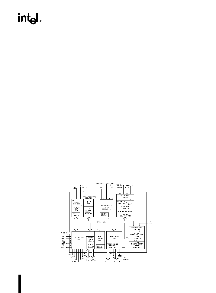
The Intel M80C186 is a CHMOS high integration microprocessor It has features which are new to the M80186
family which include a DRAM refresh control unit power-save mode and a direct numerics interface When
used in ``compatible'' mode the M80C186 is 100% pin-for-pin compatible with the NMOS M80186 (except for
M8087 applications) The ``enhanced'' mode of operation allows the full feature set of the M80C186 to be
used The M80C186 is upward compatible with M8086 and M8088 software and fully compatible with M80186
and M80188 software
270500 � 1
Figure 1 M80C186 Block Diagram
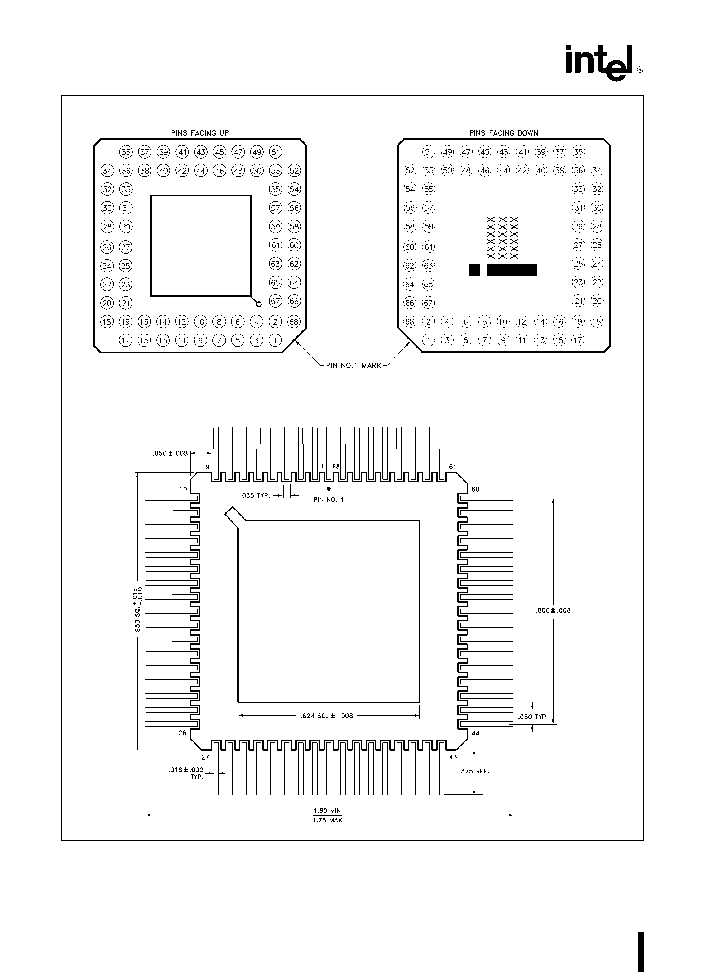
M80C186
Pin Grid Array
270500 � 30
Quad Flat Pack
270500 � 31
Figure 2 M80C186 Pinout Diagram
For additional packaging information refer to ``Packaging Outlines and Dimensions'' Order Number 231369
2
M80C186
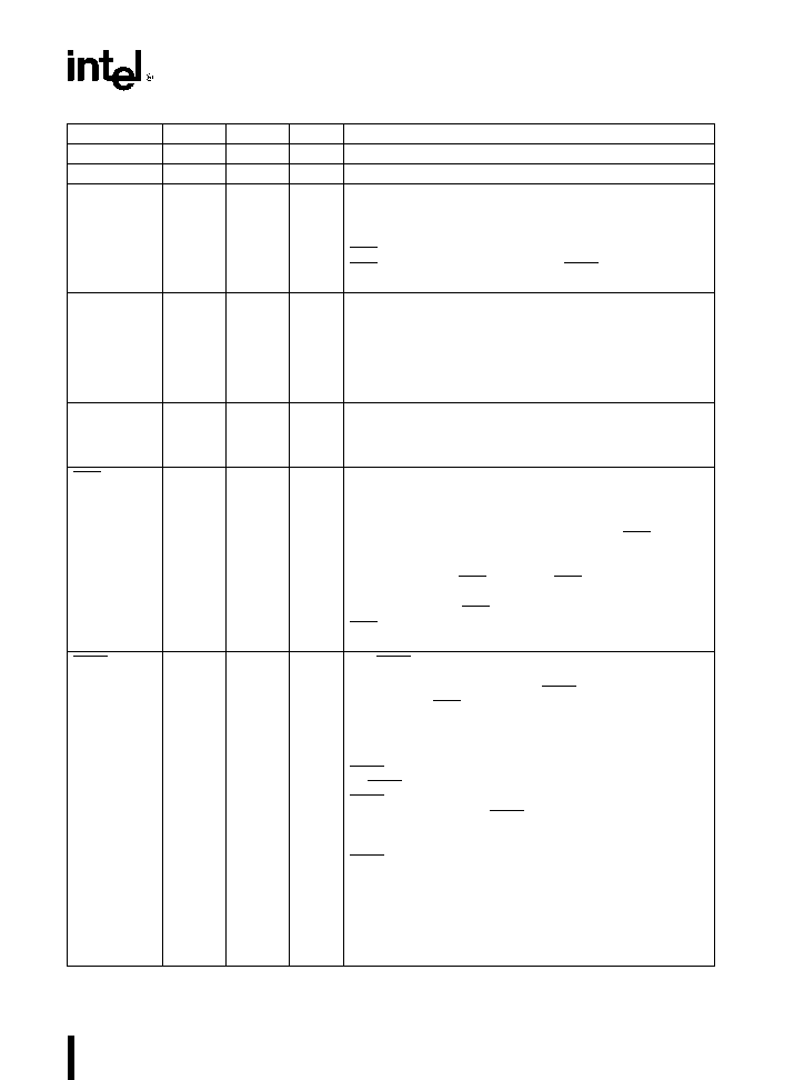
Table 1 M80C186 Pin Description
Symbol
PGA
QFP
Type
Name and Function
V
CC
V
CC
9 43
1 35
I
System Power a
5 volt power supply
V
SS
V
SS
26 60
52 18
I
System Ground
RESET
57
21
O
Reset Output indicates that the M80C186 CPU is being
reset and can be used as a system reset It is active HIGH
synchronized with the processor clock and lasts an integer
number of clock periods corresponding to the length of the
RES signal Reset goes inactive 2 clockout periods after
RES goes inactive When tied to the TEST BUSY pin Reset
forces the M80C186 into enhanced mode
X1 X2
59 58
19 20
I
Crystal Inputs X1 and X2 provide external connections for a
fundamental mode or third overtone parallel resonant crystal
for the internal oscillator X1 can connect to an external
clock instead of a crystal In this case minimize the
capacitance on X2 or drive X2 with complemented X1 The
input or oscillator frequency is internally divided by two to
generate the clock signal (CLKOUT)
CLKOUT
56
22
O
Clock Output provides the system with a 50% duty cycle
waveform All device pin timings are specified relative to
CLKOUT CLKOUT has sufficient MOS drive capabilities for
the Numeric Processor Extension
RES
24
54
I
System Reset causes the M80C186 to immediately
terminate its present activity clear the internal logic and
enter a dormant state This signal may be asynchronous to
the M80C186 clock The M80C186 begins fetching
instructions approximately 7 clock cycles after RES is
returned HIGH For proper initialization V
CC
must be within
specifications and the clock signal must be stable for more
than 4 clocks with RES held LOW RES is internally
synchronized This input is provided with a Schmitt-trigger to
facilitate power-on RES generation via an RC network When
RES occurs the M80C186 will drive the status lines to an
inactive level for one clock and then float them
TEST BUSY
47
31
I
The TEST pin is sampled during and after reset to determine
whether the M80C186 is to enter Compatible or Enhanced
Mode Enhanced Mode requires TEST to be HIGH on the
rising edge of RES and LOW four clocks later Any other
combination will place the M80C186 in Compatible Mode A
weak internal pullup insures a HIGH state when the pin is not
driven
TEST
In Compatible Mode this pin is configured to operate
as TEST This pin is examined by the WAIT instruction If the
TEST input is HIGH when WAIT execution begins instruction
execution will suspend TEST will be resampled every five
clocks until it goes LOW at which time execution will resume
If interrupts are enabled while the M80C186 is waiting for
TEST interrupts will be serviced
BUSY
In Enhanced Mode this pin is configured to operate
as BUSY The BUSY input is used to notify the M80C186 of
Numerics Processor Extension activity Floating point
instructions executing in the M80C186 sample the BUSY pin
to determine when the Numerics Processor is ready to
accept a new command BUSY is active HIGH
3
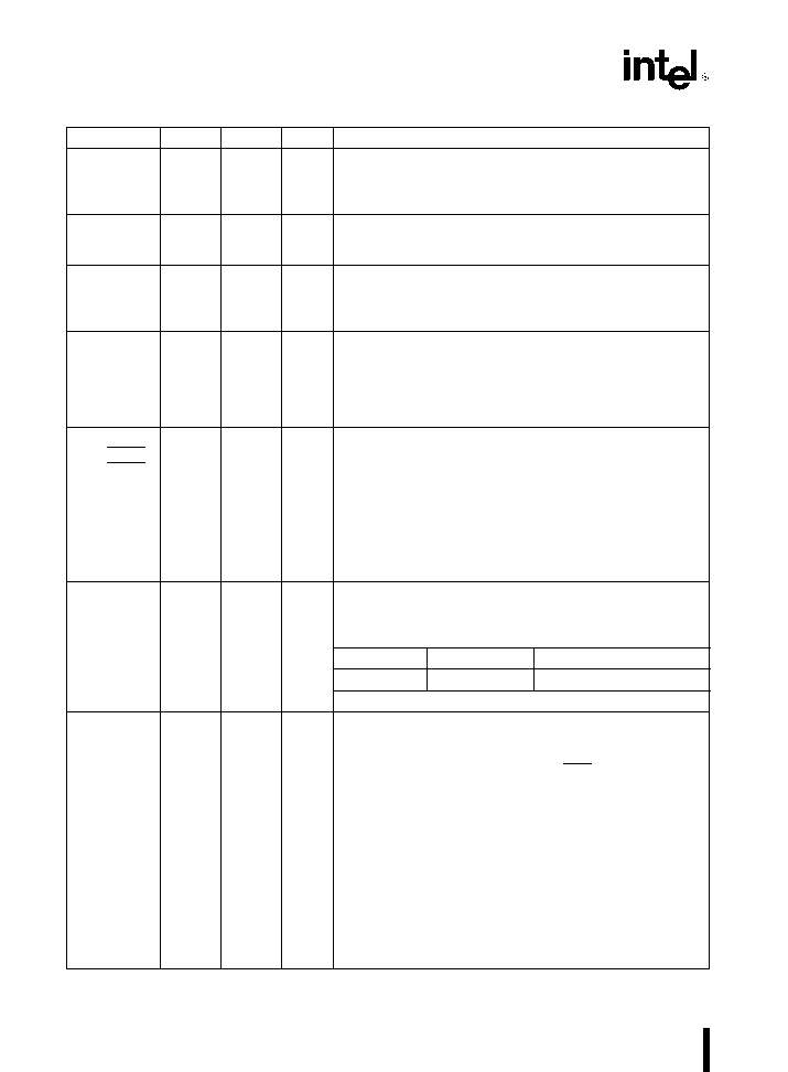
M80C186
Table 1 M80C186 Pin Description
(Continued)
Symbol
PGA
QFP
Type
Name and Function
TMR IN 1
TMR IN 0
20
21
58
57
I
I
Timer Inputs are used either as clock or control signals
depending upon the programmed timer mode These inputs
are active HIGH (or LOW-to-HIGH transitions are counted) and
internally synchronized
TMR OUT 0
TMR OUT 1
23
22
56
55
O
O
Timer outputs are used to provide single pulse or continous
waveform generation depending upon the timer mode
selected
DRQ1
DRQ0
18
19
59
60
I
I
DMA Request is driven HIGH by an external device when it
desires that a DMA channel (Channel 0 or 1) perform a
transfer These signals are active HIGH level-triggered and
internally synchronized
NMI
46
32
I
Non-Maskable Interrupt is an edge-triggered input which
causes a type 2 interrupt NMI is not maskable internally A
transition from a LOW to HIGH initiates the interrupt at the
next instruction boundary NMI is latched internally An NMI
duration of one clock or more will guarantee service This input
is internally synchronized
INT0 INT1
INT3 INTA1
INT2 INTA0
45 44
41
42
33 34
37
36
I O
I O
I
Maskable Interrupt Requests can be requested by activating
one of these pins When configured as inputs these pins are
active HIGH Interrupt Requests are synchronized internally
INT2 and INT3 may be configured via software to provide
active-LOW interrupt-acknowledge output signals All interrupt
inputs may be configured via software to be either edge- or
level-triggered To ensure recognition all interrupt requests
must remain active until the interrupt is acknowledged When
slave mode is selected the function of these pins changes
(see Interrupt Controller section of this data sheet)
A19 S6
A16 S3
A17 S4
A18 S5
65
68
67
66
13
10
11
12
O
O
O
O
Address Bus Outputs (16 � 19) and Bus Cycle Status (3 � 6)
reflect the four most significant address bits during T
1
These
signals are active HIGH During T
2
T
3
T
W
and T
4
status
information is available on these lines as encoded below
Low
High
S6
Processor Cycle
DMA Cycle
S3 S4 and S5 are defined as LOW during T
2
� T
4
AD15
1
9
I O
Address Data Bus (0 � 15) signals constitute the time
multiplexed memory or I O address (T
1
) and data (T
2
T
3
T
W
AD14
3
7
and T
4
) bus The
AD13
5
5
AD12
7
3
bus is active HIGH A
0
is analogous to BHE for the lower byte
of the data bus pins D
7
through D
0
It is LOW during T
1
when
AD11
10
68
a byte is to be transferred onto the lower portion of the bus in
AD10
12
66
memory or I O operations
AD9
14
64
AD8
16
62
AD7
2
8
AD6
4
6
AD5
6
4
AD4
8
2
AD3
11
67
AD2
13
65
AD1
15
63
AD0
17
61
4
M80C186
Table 1 M80C186 Pin Description
(Continued)
Symbol
PGA
QFP
Type
Name and Function
BHE
64
14
O
The BHE (Bus High Enable) signal is analogous to A0 in that
it is used to enable data on to the most significant half of the
data bus pins D15 � D8 BHE will be LOW during T
1
when the
upper byte is transferred and will remain LOW through T
3
AND T
W
BHE does not need to be latched BHE will float
during HOLD
In Enhanced Mode BHE will also be used to signify DRAM
refresh cycles A refresh cycle is indicated by BHE and A0
being HIGH
BHE and A0 Encodings
BHE Value
A0 Value
Function
0
0
Word Transfer
0
1
Byte Transfer on upper half
of data bus (D15 � D8)
1
0
Byte Transfer on lower half
of data bus (D
7
� D
0
)
1
1
Refresh
ALE QS0
61
17
O
Address Latch Enable Queue Status 0 is provided by the
M80C186 to latch the address ALE is active HIGH
Addresses are guaranteed to be valid on the trailing edge of
ALE The ALE rising edge is generated off the rising edge of
the CLKOUT immediately preceding T
1
of the associated bus
cycle effectively one-half clock cycle earlier than in the
standard M8086 The trailing edge is generated off the
CLKOUT rising edge in T
1
as in the M8086 Note that ALE is
never floated
WR QS1
63
15
O
Write Strobe Queue Status 1 indicates that the data on the
bus is to be written into a memory or an I O device WR is
active for T
2
T
3
and T
W
of any write cycle It is active LOW
and floats during ``HOLD '' It is driven HIGH for one clock
during Reset and then floated When the M80C186 is in
queue status mode the ALE QS0 and WR QS1 pins provide
information about processor instruction queue interaction
QS1
QS0
Queue Operation
0
0
No queue operation
0
1
First opcode byte fetched
from the queue
1
1
Subsequent byte fetched
from the queue
1
0
Empty the queue
RD QSMD
62
16
O
Read Strobe indicates that the M80C186 is performing a
memory or I O read cycle RD is active LOW for T
2
T
3
and
T
W
of any read cycle It is guaranteed not to go LOW in T
2
until after the Address Bus is floated RD is active LOW and
floats during ``HOLD'' RD is driven HIGH for one clock
during Reset and then the output driver is floated A weak
internal pull-up mechanism of the RD line holds it HIGH when
the line is not driven During RESET the pin is sampled to
determine whether the M80C186 should provide ALE WR
and RD or if the Queue-Status should be provided RD
should be connected to GND to provide Queue-Status data
5