April 1990
Order Number 271214-002
M80C186EB-16 -13 -8
16-BIT HIGH-INTEGRATION EMBEDDED PROCESSOR
Full Static Operation
True CMOS Inputs and Outputs
b
55 C to
a
125 C Operating Temperature Range
Y
Integrated Feature Set
Low-Power Static CPU Core
Two Independent UARTs each with
an Integral Baud Rate Generator
Two 8-Bit Multiplexed I O Ports
Programmable Interrupt Controller
Three Programmable 16-Bit
Timer Counters
Clock Generator
Ten Programmable Chip Selects with
Integral Wait-State Generator
Memory Refresh Control Unit
System Level Testing Support (ONCE
Mode)
Y
Direct Addressing Capability to 1 Mbyte
Memory and 64 Kbyte I O
Y
Speed Versions Available
16 MHz (M80C186EB-16)
13 MHz (M80C186EB-13)
8 MHz (M80C186EB-8)
Y
Low-Power Operating Modes
Idle Mode Freezes CPU Clocks but
keeps Peripherals Active
Powerdown Mode Freezes All
Internal Clocks
Y
Complete System Development
Support
ASM86 Assembler PL M 86 Pascal
86 Fortran 86 C-86 and System
Utilities
In-Circuit Emulator (ICE
TM
-186EB)
Y
Supports M80C187 Numeric
Coprocessor Interface
Y
Available In
88-Lead Pin Grid Array
(MG80C186EB)
The M80C186EB is a second generation CHMOS High-Integration microprocessor It has features that are
new to the M80C186 family and include a STATIC CPU core an enhanced Chip Select decode unit two
independent Serial Channels I O ports and the capability of Idle or Powerdown low power modes
271214 � 1

M80C186EB-16 -13 -8
16-Bit High-Integration Embedded Processor
CONTENTS
PAGE
INTRODUCTION
4
OVERVIEW
4
M80C186EB Core Architecture
4
Register Set
4
Instruction Set
5
Memory Organization
5
Addressing Modes
5
Data Types
7
Interrupts
7
Bus Interface Unit
9
Clock Generator
9
M80C186EB Peripheral Architecture
10
Interrupt Control Unit
10
Timer Counter Unit
10
Serial Communications Unit
12
Chip-Select Unit
12
I O Port Unit
13
Refresh Control Unit
13
Power Management Unit
13
M80C187 Interface
13
ONCE Test Mode
13
PACKAGE INFORMATION
14
Pin Descriptions
14
M80C186EB PINOUT
19
ELECTRICAL SPECIFICATIONS
21
Absolute Maximum Ratings
21
OPERATING CONDITIONS
21
RECOMMENDED CONNECTIONS
21
DC SPECIFICATIONS
22
I
CC
versus Frequency and Voltage
23
PDTMR Pin Delay Calculation
23
CONTENTS
PAGE
AC SPECIFICATIONS
24
AC Characteristics
M80C186EB-16
24
AC Characteristics
M80C186EB-13
25
AC Characteristics
M80C186EB-8
26
Relative Timings
(M80C186EB-16 -13 -8)
27
Serial Port Mode 0 Timings
(M80C186EB-16 -13 -8)
28
AC TEST CONDITIONS
29
AC TIMING WAVEFORMS
29
DERATING CURVES
32
RESET
33
COLD RESET WAVEFORMS
34
WARM RESET WAVEFORMS
35
BUS CYCLE WAVEFORMS
36
REGISTER BIT SUMMARY
44
M80C186EB EXECUTION TIMINGS
48
INSTRUCTION SET SUMMARY
49
FOOTNOTES
54
88-LEAD CERAMIC PIN GRID ARRAY
PACKAGE
55
ERRATA
56
REVISION HISTORY
56
2
M80C186EB
271214 � 2
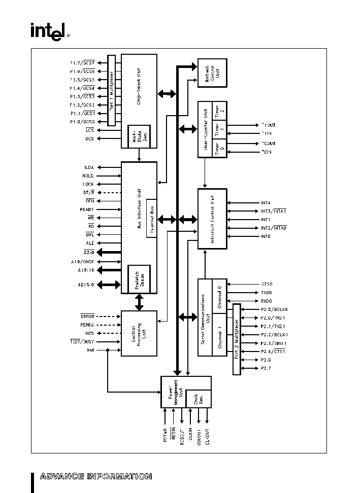
Figure 1 M80C186EB Block Diagram
3
M80C186EB
INTRODUCTION
The M80C186EB is the first product in a new gener-
ation of low-power high-integration microproces-
sors It enhances the existing 186 family by offering
new features and new operating modes
The
M80C186EB is object code compatible with the
M80C186 M80C188 microprocessors
The feature set of the M80C186EB meets the needs
of low power space critical applications Low-Power
applications benefit from the static design of the
CPU core and the integrated peripherals Minimum
current consumption is achieved by providing a Pow-
erdown mode that halts operation of the device and
freezes the clock circuits Peripheral design en-
hancements ensure that non-initialized peripherals
consume little current
Space critical applications benefit from the inte-
gration of commonly used system peripherals Two
serial channels are provided for services such as
diagnostics inter-processor communication modem
interface terminal display interface and many oth-
ers A flexible chip select unit simplifies memory and
peripheral interfacing The interrupt unit provides
sources for up to 129 external interrupts and will pri-
oritize these interrupts with those generated from
the on-chip peripherals Three general purpose tim-
er counters and sixteen multiplexed I O port pins
round out the feature set of the M80C186EB
OVERVIEW
Figure 1 shows a block diagram of the M80C186EB
The Execution Unit (EU) is an enhanced M8086
CPU core that includes
dedicated hardware to
speed up effective address calculations enhance
execution speed for multiple-bit shift and rotate in-
structions and for multiply and divide instructions
string move instructions that operate at full bus
bandwidth ten new instruction and full static opera-
tion The Bus Interface Unit (BIU) is the same as that
found on the original 186 family products except the
queue-status mode has been deleted and buffer in-
terface control has been changed to ease system
design timings An independent internal bus is used
to allow communication between the BIU and inter-
nal peripherals
M80C186EB Core Architecture
REGISTER SET
The
M8086
M8088
M80186
M80C186
and
M80C188 all contain the same basic set of registers
instructions
and
addressing
modes
The
M80C186EB is upward compatible with all of these
microprocessors
The M80C186EB base architecture has fourteen
16-bit registers as shown in Figure 2 There are eight
general purpose registers which may be used for
arithmetic and logic operands Four of these regis-
ters (AX BX CX and DX) can be used as 16-bit
registers or split into pairs of separate 8-bit registers
The other four registers (BP SI DI and SP) may also
be used to determine offset addresses of operands
in memory These registers may contain base ad-
dresses or indexes to particular locations within a
segment The addressing mode selects the specific
registers for operand and address calculations
Another four 16-bit registers (CS DS ES SS) select
the segments of memory that are immediately ad-
dressable for code stack and data There are two
remaining special purpose registers (IP and F) that
record or alter certain aspects of the M80C186EB
processor state
15
0
AH
AL
AX
BH
BL
BX
CH
CL
CX
DH
DL
DX
Source Index
SI
Destination Index
DI
Base Pointer
BP
Stack Pointer
SP
Code Segment
CS
Stack Segment
SS
Data Segment
DS
Extra Segment
ES
Instruction Pointer
IP
Flags
F
Figure 2 M80C186EB Register Set
4
M80C186EB
INSTRUCTION SET
The instruction set is divided into seven categories
data transfer arithmetic shift rotate logical string
manipulation
control transfer
high-level instruc-
tions and processor control These categories are
summarized in Figure 4
An M80C186EB instruction can reference anywhere
from zero to several operands An operand can
reside in a register in the instruction itself or in
memory
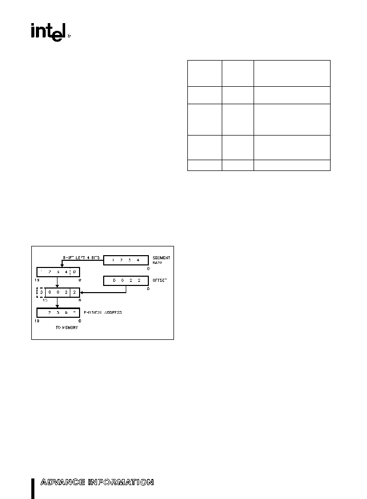
MEMORY ORGANIZATION
Memory is organized in sets of segments Each seg-
ment is a linear contiguous sequence of up to 64K
(2
16
) 8-bit bytes Memory is addressed using a two-
component address (a pointer) that consists of a
16-bit base segment and a 16-bit offset The 16-bit
base segment values are contained in one of four
internal segment registers (code data stack extra)
The physical address is calculated by shifting the
base value left by four bits and adding the 16-bit
offset value to yield a 20-bit physical address (see
Figure 3) The resulting 20-bit address allows for a
1 Mbyte address range
271214 � 3
Figure 3 Two Component Address
All instructions that address operands in memory
must specify the base segment and the 16-bit offset
value For speed and compact instruction encoding
the segment register used for a physical address
generation is implied by the addressing mode used
(see Table 1) Special segment override instruction
prefixes allow the implicit segment register selection
rules to be overridden for special cases The code
stack data and extra segments may coincide for
simple programs
Table 1 Segment Register Selection Rules
Memory
Segment
Implicit Segment
Reference
Register
Selection Rule
Needed
Used
Instructions Code (CS) Instruction prefetch and
immediate data
Stack
Stack (SS) All stack pushes and pops
any memory references
which use the BP register
as a base
External
Extra (ES) All String instruction
references which use the
DI register as an index
Local Data Data (DS) All other data references
ADDRESSING MODES
The M80C186EB provides eight categories of ad-
dressing modes to specify operands Two address-
ing modes are provided for instructions that operate
on register or immediate operands
Register Operand Mode
The operand is located
in one of the 8- or 16-bit general registers
Immediate Operand Mode
The operand is in-
cluded in the instruction
Six modes are provided to specify the location of an
operand in a memory segment A memory operand
address consists of two 16-bit components a seg-
ment base and an offset The segment base is sup-
plied by a 16-bit segment register either implicitly
chosen by the addressing mode or explicitly chosen
by a segment override prefix The offset also called
the effective address is calculated by summing any
combination of the following three address ele-
ments
the
displacement
(an 8- or 16-bit immediate value
contained in the instruction)
the
base
(contents of either the BX or BP base
registers) and
the
index
(contents of either the SI or DI index
registers)
5

M80C186EB
GENERAL PURPOSE
MOV
PUSH
POP
PUSHA
POPA
XCHG
XLAT
INPUT OUTPUT
IN
OUT
ADDRESS OBJECT
LEA
LDS
LES
FLAG TRANSFER
LAHF
SAHF
PUSHF
POPF
ADDITION
ADD
INC
AAA
DAA
SUBSTRACTION
SUB
SBB
DEC
NEG
CMP
AAS
DAS
MULTIPLICATION
MUL
IMUL
AAM
DIVISION
DIV
IDIV
AAD
CBW
CWD
STRING OPERATIONS
MOVS
INS
OUTS
CMPS
SCAS
LODS
STOS
REP
REPE REPZ
REPNE REPNZ
LOGICALS
NOT
AND
OR
XOR
TEST
SHIFTS
SHL SAL
SHR
SAR
ROTATES
ROL
ROR
RCL
RCR
FLAG OPERATIONS
STC
CLC
CMC
STD
CLD
STI
CLI
EXTERNAL
SYNCHRONIZATION
HLT
WAIT
LOCK
NO OPERATION
NOP
HIGH LEVEL INSTRUCTIONS
ENTER
LEAVE
BOUND
CONDITIONAL TRANSFERS
JA JNBE
JAE JNB
JB JNAE
JBE JNA
JC
JE JZ
JG JNLE
JGE JNL
JL JNGE
JLE JNG
JNC
JNE JNZ
JNO
JNP JP0
JNS
JO
JP JPE
JS
UNCONDITIONAL TRANSFERS
CALL
RET
JMP
ITERATION CONTROLS
LOOP
LOOPE LOOPZ
LOOPNE LOOPNZ
JCXZ
INTERRUPTS
INT
INTO
IRET
Figure 4 M80C186EB Instruction Set
6

M80C186EB
Any carry out from the 16-bit addition is ignored
8-bit displacements are sign extended to 16-bit val-
ues
Combinations of these three address elements de-
fine the six memory addressing modes described
below
Direct Mode
The operand's offset is contained in
the instruction as an 8- or 16-bit displacement el-
ement
Register Indirect Mode
The operand's offset is in
one of the registers SI DI BX or BP
Based Mode
The operand's offset is the sum of
an 8- or 16-bit displacement and the contents of
a base register (BX or BP)
Indexed Mode
The operand's offset is the sum
of an 8- or 16-bit displacement and the contents
of an index register (SI or DI)
Based Indexed Mode
The operand's offset is the
sum of the contents of a base register and an
index register
Based Indexed Mode with Displacement
The op-
erand's offset is the sum of a base register's con-
tents an index register's contents and an 8- or
16-bit displacement
DATA TYPES
The M80C186EB directly supports the following data
types
Integer
A signed binary numeric value contained
in an 8-bit byte or 16-bit word All operations as-
sume a 2's complement representation Signed
32- and 64-bit integers are supported using the
M80C187 Numerics Coprocessor
Ordinal
An unsigned binary numeric value con-
tained in an 8-bit byte or 16-bit word
Pointer
A 16- or 32-bit quantity composed of a
16-bit offset component or a 16-bit segment
base component and a 16-bit offset component
String
A contiguous sequence of bytes or words
A string may contain from 1 Kbyte to 64 Kbytes
ASCII
A byte representation of alphanumeric and
control characters using the ASCII standard of
character representation
BCD
A byte (unpacked) representation of the
decimal digits 0 � 9
Packed BCD
A byte (packed) representation of
two decimal digits (0 � 9) One digit is stored in
each nibble (4 bits) of the byte
Floating Point
A signed 32- 64- or 80-bit real
number representation Floating point operands
are supported when using the M80C187 Numeric
Coprocessor
In general individual data elements must fit within
defined segment limits
INTERRUPTS
An interrupt transfers execution to a new program
location The old program address (CS IP) and ma-
chine state (F) are saved on the stack to allow re-
sumption of the interrupted program Interrupts fall
into three classes hardware initiated software (pro-
gram) initiated and instruction exception initiated
Hardware initiated interrupts occur in response to an
external or internal input and are classified as non-
maskable or maskable
Programs may cause an interrupt by executing the
``INT'' instruction Instruction exceptions occur when
an illegal opcode has been fetched into the queue
and is read by the execution unit Another type of
exception can be generated when executing an
``ESC'' instruction
For all cases except the ``ESC'' exception the return
address from an exception will point at the instruc-
tion immediately following the instruction causing
the exception The return address after an ``ESC''
exception will point back to the ESC instruction
causing the exception or to the segment override
prefix immediately preceding the ESC instruction if
the prefix was present
A table containing up to 256 pointers defines the
proper interrupt service routine for each interrupt In-
terrupts 0 � 31 are reserved by Intel Table 2 shows
the M80C186EB predefined type and default priority
levels For each interrupt an 8-bit vector (Vector
Type) identifies the appropriate table entry Multiply-
ing the 8-bit vector by 4 defines the vector address
INT instructions contain or imply the vector type and
allow access to all 256 interrupts
7

M80C186EB
Table 2 M80C186EB Interrupt Vectors
Interrupt
Vector
Vector
Default
Related
Name
Type
Address
Priority
Instructions
Divide Error
0
00H
1
DIV IDIV
Single Step Interrupt
1
04H
1A
All
Non-Maskable Interrupt
2
08H
1
INT 2 or NMI
One Byte Interrupt
3
0CH
1
INT
Interrupt on Overflow
4
10H
1
INT0
Array Bounds Check
5
14H
1
BOUND
Invalid OP-Code
6
18H
1
Illegal Inst
ESC OP-Code Interrupt
7
1CH
1
ESC OP-Codes
Timer 0 Interrupt
8
20H
2
Reserved
9 � 11
24H � 2CH
INT0 Interrupt
12
30H
5
INT1 Interrupt
13
34H
6
INT2 Interrupt
14
38H
7
INT3 Interrupt
15
3CH
8
Numerics Exception
16
40H
1
ESC OP-Codes
INT4 Interrupt
17
44H
4
Timer1 Interrupt
18
48H
2A
Timer2 Interrupt
19
4CH
2B
UART 0 Receive Interrupt
20
50H
3
UART 0 Transmit Interrupt
21
54H
3A
Reserved
22 � 31
58H � 7CH
8

M80C186EB
BUS INTERFACE UNIT
The M80C186EB core incorporates a bus controller
that generates local bus control signals In addition
it employs a HOLD HLDA protocol to share the local
bus with other bus masters
The bus controller is responsible for generating 20
bits of address read and write strobes bus cycle
status information and data (for write operations) in-
formation It is also responsible for reading data off
the local bus during a read operation A READY in-
put pin is provided to extend a bus cycle beyond the
minimum four states (clocks)
A HOLD HLDA protocol is provided by the local bus
controller to allow multiple bus masters to share the
same local bus When the M80C186EB relinquishes
control of the local bus it floats certain bus control
signals to allow another bus master to drive these
pins directly Refer to the Pin Description section to
determine which pins the M80C186EB will float dur-
ing a HOLD HLDA bus exchange
The M80C186EB local bus controller also generates
two control signals (DEN and DT R) when interfac-
ing to external transceiver chips This capability al-
lows the addition of transceivers for simple buffering
of the mulitplexed address data bus
CLOCK GENERATOR
The M80C186EB provides an on-chip clock genera-
tor for both internal and external clock generation
The clock generator features a crystal oscillator a
divide-by-two counter and two low-power operating
modes
The oscillator circuit is designed to be used with ei-
ther a parallel resonant fundamental or third-over-
tone mode crystal network Alternatively the oscilla-
tor circuit may be driven from an external clock
source Figure 5 shows the various operating modes
of the M80C186EB oscillator circuit
The crystal or clock frequency chosen must be twice
the required processor operating frequency due to
the internal divide-by-two counter This counter is
used to drive all internal phase clocks and the exter-
nal CLKOUT signal CLKOUT is a 50% duty cycle
processor clock and can be used to drive other sys-
tem components All AC timings are referenced to
CLKOUT
The following parameters are recommended when
choosing a crystal
Temperature Range
Application Specific
ESR (Equivalent Series Resistance)
40X max
C0 (Shunt Capacitance of Crystal)
7 0 pF max
C
L
(Load Capacitance)
20 pF
g
2 pF
Drive Level
1 mW max
271214 � 4
(A) Crystal Connection
NOTE
The L
1
C
1
network is only required when using a third-
overtone crystal
271214 � 5
(B) Clock Connection
Figure 5 M80C186EB Clock Configurations
9

M80C186EB
M80C186EB Peripheral Architecture
The M80C186EB has integrated several common
system peripherals with a CPU core to create a com-
pact yet powerful system The integrated peripher-
als are designed to be flexible and provide logical
interconnections between supporting units (e g the
interrupt control unit supports interrupt requests
from the timer counters or serial channels)
The list of integrated peripherals include
7-Input Interrupt Control Unit
3-Channel Timer Counter Unit
2-Channel Serial Communications Unit
10-Output Chip-Select Unit
I O Port Unit
Refresh Control Unit
Power Management Unit
The registers associated with each integrated peri-
heral are contained within a 128 x 16 register file
called the Peripheral Control Block (PCB) The PCB
can be located in either memory or I O space on
any 256 Byte address boundary During bus cycles
that access the PCB the bus controller will signal
the operation externally (i e
the RD WR status
address data etc lines will be driven as in a normal
bus cycle) However READY is ignored and the con-
tents of the data bus during a read operation is ig-
nored
The starting address of the PCB is controlled by a
relocation register and can overlap any of the mem-
ory or I O regions programmed into the Chip Select
Unit In this case the overlapped chip select will not
go active when the PCB is read or written
Figure 6 provides a list of the registers associated
with the PCB The Register Bit Summary at the end
of this specification individually lists all of the regis-
ters and identifies each of their programming attri-
butes
INTERRUPT CONTROL UNIT
The M80C186EB can receive interrupts from a num-
ber of sources both internal and external The inter-
rupt control unit serves to merge these requests on
a priority basis for individual service by the CPU
Each interrupt source can be independently masked
by the Interrupt Control Unit (ICU) or all interrupts
can be globally masked by the CPU
Internal interrupt sources include the Timers and Se-
rial channel 0 External interrupt sources come from
the five input pins INT4 0 The NMI interrupt pin is
not controlled by the ICU and is passed directly to
the CPU Although the Timer and Serial channel
each have only one request input to the ICU sepa-
rate vector types are generated to service individual
interrupts within the Timer and Serial channel units
The M80C186EB ICU provides a mechanism for ex-
panding the number of external interrupt sources
Two pairs of pins can be independently configured
to support an external slave interrupt controller
(82C59A) Each pair of external pins can be expand-
ed to support 64 interrupts making it possible for the
M80C186EB to support a total of 129 external inter-
rupts
The ICU may be used in a polled mode if interrupts
are undesirable When polling the processor dis-
ables interrupts and then polls the ICU whenever it is
convenient
TIMER COUNTER UNIT
The M80C186EB Timer Counter Unit (TCU) pro-
vides three 16-bit programmable timers Two of
these are highly flexible and are connected to exter-
nal pins for control or clocking A third timer is not
connected to any external pins and can only be
clocked internally However it can be used to clock
the other two timer channels The TCU can be used
to count external events time external events gen-
erate non-repetitive waveforms generate timed in-
terrupts etc
Each timer has at least one 16-bit compare register
and one 16-bit count register Timers 0 and 1 each
have an additional 16-bit compare register The
count register is incremented every fourth CPU clock
cycle (internal clocking) every time Timer2 expires
(Timers 0 and 1 only) or every Low-to-High tran-
sition on the timer input pin (Timers 0 and 1 only)
The input clock to Timers 0 and 1 must not exceed
one
fourth
the
operating
frequency
of
the
M80C186EB When the count register matches the
value programmed into the compare register sever-
al operations may happen
All three timers can generate an interrupt when the
compare register matches the value in the count
register Additionally Timers 0 and 1 have an output
pin that can change state or pulse when the com-
pare condition occurs
10

M80C186EB
PCB
Function
Offset
00H
Reserved
02H
End Of Interrupt
04H
Poll
06H
Poll Status
08H
Interrupt Mask
0AH
Priority Mask
0CH
In-Service
0EH
Interrupt Request
10H
Interrupt Status
12H
Timer Control
14H
Serial Control
16H
INT4 Control
18H
INT0 Control
1AH
INT1 Control
1CH
INT2 Control
1EH
INT3 Control
20H
Reserved
22H
Reserved
24H
Reserved
26H
Reserved
28H
Reserved
2AH
Reserved
2CH
Reserved
2EH
Reserved
30H
Timer0 Count
32H
Timer0 Compare A
34H
Timer0 Compare B
36H
Timer0 Control
38H
Timer1 Count
3AH Timer1 Compare A
3CH Timer1 Compare B
3EH
Timer1 Control
PCB
Function
Offset
40H
Timer2 Count
42H
Timer2 Compare
44H
Reserved
46H
Timer2 Control
48H
Reserved
4AH
Reserved
4CH
Reserved
4EH
Reserved
50H
Reserved
52H
Port0 Pin
54H
Port0 Control
56H
Port0 Latch
58H
Port1 Direction
5AH
Port1 Pin
5CH
Port1 Control
5EH
Port1 Latch
60H
Serial0 Baud
62H
Serial0 Count
64H
Serial0 Control
66H
Serial0 Status
68H
Serial0 RBUF
6AH
Serial0 TBUF
6CH
Reserved
6EH
Reserved
70H
Serial1 Baud
72H
Serial1 Count
74H
Serial1 Control
76H
Serial1 Status
78H
Serial1 RBUF
7AH
Serial1 TBUF
7CH
Reserved
7EH
Reserved
PCB
Function
Offset
80H
GCS0 Start
82H
GCS0 Stop
84H
GCS1 Start
86H
GCS1 Stop
88H
GCS2 Start
8AH
GCS2 Stop
8CH
GCS3 Start
8EH
GCS3 Stop
90H
GCS4 Start
92H
GCS4 Stop
94H
GCS5 Start
96H
GCS5 Stop
98H
GCS6 Start
9AH
GCS6 Stop
9CH
GCS7 Start
9EH
GCS7 Stop
A0H
LCS Start
A2H
LCS Stop
A4H
UCS Start
A6H
UCS Stop
A8H
Relocation
AAH
Reserved
ACH
Reserved
AEH
Reserved
B0H
Refresh Base
B2H
Refresh Time
B4H
Refresh Control
B6H
Refresh Address
B8H
Power Control
BAH
Reserved
BCH
Step ID
BEH
Reserved
PCB
Function
Offset
C0H
Reserved
C2H
Reserved
C4H
Reserved
C6H
Reserved
C8H
Reserved
CAH
Reserved
CCH
Reserved
CEH
Reserved
D0H
Reserved
D2H
Reserved
D4H
Reserved
D6H
Reserved
D8H
Reserved
DAH
Reserved
DCH
Reserved
DEH
Reserved
E0H
Reserved
E2H
Reserved
E4H
Reserved
E6H
Reserved
E8H
Reserved
EAH
Reserved
ECH
Reserved
EEH
Reserved
F0H
Reserved
F2H
Reserved
F4H
Reserved
F6H
Reserved
F8H
Reserved
FAH
Reserved
FCH
Reserved
FEH
Reserved
Figure 6 M80C186EB Peripheral Control Block Registers
11

M80C186EB
Other timer programming options include
All three timers can be set to halt or continue
after a compare match
Timers 0 and 1 can be reset or retriggered using
their respective input pins
TCU registers can be read or written at any time
SERIAL COMMUNICATIONS UNIT
The Serial Control Unit (SCU) of the M80C186EB
contains two independent channels Each channel is
identical in operation except that only channel 0 is
supported by the integrated interrupt controller
(channel 1 has an external interrupt pin) Each
channel has its own baud rate generator that is in-
dependent of the Timer Counter Unit and can be
internally or externally clocked at up to one half the
M80C186EB operating frequency
Each serial channel supports one synchronous and
four asynchronous modes of operation and is com-
patible with the serial ports of the MCS -51 and
MCS -96 family of products Data field length can
be 7- 8- or 9-bits with optional odd or even parity
(generated and checked) and one stop bit (generat-
ed and checked) The 9-bit mode has an optional
``addressing'' feature to simplify interprocessor com-
munication Each serial port is doubled buffered in
both transmit and receive operation (data can be
read or written to a buffer register while data is shift-
ed into or out of a shifting register respectively)
A Clear-To-Send input pin can be programmed to
prevent data transmission if the pin is sampled inac-
tive Serial channel 0 is supported by the integrated
interrupt controller providing separate receive and
transmit vector types Serial channel 1 has an exter-
nal interrupt pin which OR's the receive and transmit
interrupts This external interrupt pin can be routed
to either the external pins of the ICU the NMI pin or
any other external system interrupt controller Status
bits are provided to allow polling of the serial chan-
nels if interrupts are not desired
Independent baud rate generators are provided for
each of the serial channels For the asynchronous
modes the generator supplies an 8x baud clock to
both the receive and transmit register logic A 1x
baud clock is provided in the synchronous mode
Additional features of the SCU include
Framing error receive buffer overrun error and
parity error detection
Break detect
Break send
CHIP-SELECT UNIT
The M80C186EB Chip-Select Unit (CSU) integrates
logic which provides up to ten programmable chip-
selects to access both memories and peripherals In
addition each chip-select can be programmed to
automatically insert additional clocks (wait-states)
into the current bus cycle and automatically termi-
nate a bus cycle independent of the condition of the
READY input pin
Each of the chip-selects can be programmed to go
active for either memory or I O accesses UCS is
the only chip-select that is active after a reset and is
enabled for memory addresses in the range
0FFC00H to 0FFFFFH (this allows a boot-ROM to
be accessed using UCS) Every chip-select has a
programmable start and stop register that defines
the active region for the chip-select and the ready
characteristics for the region
The start and stop address fields are 10 bits in
length and are matched against the upper 10 bits of
either the memory or I O address A 10-bit compare
results in a granularity of 1 Kbytes for memory ac-
cesses and 64 bytes for I O accesses Each chip
select can be disabled by programming its start ad-
dress greater than its stop address or by clearing its
enable bit
Each chip-select can be programmed to automati-
cally insert wait-states and to control whether the
external READY input is to be ignored or used The
M80C186EB bus controller will wait the programmed
number of wait-states before the external READY
pin can be used to extend or terminate the bus cy-
cle
Overlapping of chip-selects is allowed However
each one that overlaps will go active If any overlap-
ping chip-select has been programmed to use exter-
nal ready the bus control unit will insert the least
amount of programmed wait-states programmed be-
fore the external ready pin is used If all overlapped
chip-selects ignore external ready the bus controller
will insert the maximum number of programmed
wait-states Any chip-select that overlaps the Periph-
eral Control Block (PCB) will not go active for that
portion of the address range allocated to the PCB
12

M80C186EB
The Generic Chip-Selects (GCS7 0) are multiplexed
with an output only Port function Any channel that is
being used as a chip-select must be disabled as a
port pin by correctly programming the port pin con-
trol registers (see the following section)
I O PORT UNIT
The I O Port Unit (IPU) on the M80C186EB supports
two 8-bit channels of input output or input output
operation Port 1 is multiplexed with the chip select
pins and is output only Most of Port 2 is multiplexed
with the serial channel pins Port 2 pins are limited to
either an output or input function depending on the
operation of the serial pin it is multiplexed with
Two bits of Port 2 are not multiplexed with any other
peripheral functions and can be used as either an
input or an output function A port direction register
is used to define the function of the port pin The
output for these two pins are open drain
Besides a direction register each port channel has a
data latch register port pin register and a port multi-
plexer control register
REFRESH CONTROL UNIT
The Refresh Control Unit (RCU) automatically gen-
erates a periodic memory read bus cycle to keep
dynamic or pseudo-static memory refreshed A 9-bit
counter controls the number of clocks between re-
fresh requests
A 12-bit address generator is maintained by the RCU
and is presented on the A12 1 address lines during
the refresh bus cycle The address generator is in-
cremented only after the refresh bus cycle is run
This ensures that all address combinations will be
presented to the memory array even if the refresh
bus cycle is not run before another request is gener-
ated Address bits A19 13 are programmable to al-
low the refresh address block to be located on any 8
Kbyte boundary
The chip-select unit is active during refresh bus cy-
cles This means that a chip-select will go active if
the refresh address is within the limits specified for
the channel In addition BHE and A0 are both driven
high during refresh bus cycles (this is normally an
invalid bus condition) Data on the AD15 0 bus is
ignored
A pending refresh request will attempt to abort a
HOLD HLDA bus exchange HLDA is deasserted
when a refresh request is pending and a bus HOLD
is already in progress HOLD must then be released
in order for the M80C186EB to execute the refresh
bus cycle
POWER MANAGEMENT UNIT
The M80C186EB Power Management Unit (PMU) is
provided to control the power consumption of the
device The PMU provides three power modes Ac-
tive Idle and Powerdown
Active
Mode
indicates
that
all
units
on
the
M80C186EB are functional and the device con-
sumes maximum power (depending on the level of
peripheral operation) Idle Mode freezes the clocks
of the Execution and Bus units at a logic zero state
(all peripherals continue to operate normally) An un-
masked interrupt
NMI
or reset will cause the
M80C186EB to exit the Idle mode
The Powerdown mode freezes all internal clocks at
a logic zero level and disables the crystal oscillator
All internal registers hold their values provided V
CC
is maintained Current consumption is reduced to
just transistor junction leakage An NMI or processor
reset will cause the M80C186EB to exit the Power-
down Mode A timing pin is provided to establish the
length of time between exiting Powerdown and re-
suming device operation (Length of time depends
on startup time of crystal oscillator and is application
dependent )
M80C187 Interface
The M80C186EB supports the direct connection of
the M80C187 Numerics Coprocessor
ONCE Test Mode
To facilitate testing and inspection of devices when
fixed into a target system the M80C186EB has a
test mode available which forces all output and in-
put output pins to be placed in the high-impedance
state ONCE stands for ``ON Circuit Emulation'' The
ONCE mode is selected by forcing the A19 ONCE
pin LOW (0) during a processor reset (this pin is
weakly held to a HIGH (1) level) while RESIN is ac-
tive
13
M80C186EB
PACKAGE INFORMATION
This section describes the pins pinouts and thermal
characteristics for the M80C186EB PGA package
For complete package specifications and informa-
tion see the Intel Packaging Outlines and Dimen-
sions Guide (Order Number 231369)
Pin Descriptions
The M80C186EB pins are described in this section
Table 3 presents the legend for interpreting the pin
descriptions in Table 4 Figure 7 provides an exam-
ple pin description entry The ``I O'' signifies that the
pins are bidirectional (i e
have both an input and
output function) The ``S'' indicates that as an input
the signal is synchronized to CLKOUT for proper op-
eration The ``H(Z)'' indicates that these pins will
float while the processor is in the Hold Acknowledge
state R(Z) indicates that these pins will float while
RESIN is low P(X) Indicates that these pins will re-
tain its current value when Idle or Powerdown
Modes are entered
All pins float while the processor is in the ONCE
Mode except OSCOUT (OSCOUT is required for
crystal operation)
Name
Type
Description
AD15 0
I O
These pins provide a multiplexed
S(L)
ADDRESS and DATA bus During
H(Z) the address phase of the bus
R(Z) cycle address bits 0 through 15
P(X) are presented on the bus and can
be latched using ALE 8- or 16-bit
data information are transferred
during the data phase of the bus
cycle
Figure 7 Example Pin Description Entry
Table 3 Pin Description Nomenclature
Symbol
Description
I
Input Only Pin
O
Output Only Pin
I O
Pin can be either input or output
Pin ``must be'' connected as described
S( )
Synchronous Input must meet setup and
hold times for proper operation of the
processor The pin is
S(E) edge sensitive
S(L) level sensitive
A( )
Asynchronous Input must meet setup and
hold only to guarantee recognition The
pin is
A(E) edge sensitive
A(L) level sensitive
H( )
While the processor's bus is in the Hold
Acknowledge state the pin
H(1) is driven to V
CC
H(0) is driven to V
SS
H(Z) floats
H(Q) remains active
H(X) retains current state
R( )
While the processor's RES line is low the
pin
R(1) is driven to V
CC
R(0) is driven to V
SS
R(Z) floats
R(WH) weak pullup
R(WL) weak pulldown
P( )
While Idle or Powerdown modes are
active the pin
P(1) is driven to V
CC
P(0) is driven to V
SS
P(Z) floats
P(Q) remains active
(1)
P(X) retains current state
NOTE
1
Any pin that specifies P(Q) are valid for Idle
Mode All pins are P(X) for Powerdown Mode
14

M80C186EB
Table 4 M80C186EB Pin Descriptions
Name
Type
Description
V
CC
POWER
connections consist of four pins which must be shorted
externally to a V
CC
board plane
V
SS
GROUND
connections consist of six pins which must be shorted
externally to a V
SS
board plane
CLKIN
I
CLocK INput
is an input for an external clock An external oscillator
operating at two times the required M80C186EB operating frequency
A(E)
can be connected to CLKIN For crystal operation CLKIN (along with
OSCOUT) are the crystal connections to an internal Pierce oscillator
OSCOUT
O
OSCillator OUTput
is only used when using a crystal to generate the
external clock OSCOUT (along with CLKIN) are the crystal
H(Q)
connections to an internal Pierce oscillator This pin is not to be used
R(Q)
as 2X clock output for non-crystal applications (i e this pin is N C for
P(Q)
non-crystal applications) OSCOUT does not float in ONCE mode
CLKOUT
O
CLocK OUTput
provides a timing reference for inputs and outputs of
the processor and is one-half the input clock (CLKIN) frequency
H(Q)
CLKOUT has a 50% duty cycle and transistions every falling edge of
R(Q)
CLKIN
P(Q)
RESIN
I
RESet IN
causes the M80C186EB to immediately terminate any bus
cycle in progress and assume an initialized state All pins will be
A(L)
driven to a known state and RESOUT will also be driven active The
rising edge (low-to-high) transition synchronizes CLKOUT with CLKIN
before the M80C186EB begins fetching opcodes at memory location
0FFFF0H
RESOUT
O
RESet OUTput
that indicates the M80C186EB is currently in the
reset state RESOUT will remain active as long as RESIN remains
H(0)
active
R(1)
P(0)
PDTMR
I O
Power-Down TiMeR
pin (normally connected to an external
capacitor) that determines the amount of time the M80C186EB waits
A(L)
after an exit from power down before resuming normal operation The
H(WH)
duration of time required will depend on the startup characteristics of
R(Z)
the crystal oscillator
P(1)
NMI
I
Non-Maskable Interrupt
input causes a TYPE-2 interrupt to be
serviced by the CPU NMI is latched internally
A(E)
TEST BUSY
I
TEST
is used during the execution of the WAIT instruction to
suspend CPU operation until the pin is sampled active (LOW) TEST
A(E)
is alternately known as BUSY when interfacing with an M80C187
numerics coprocessor
AD15 0
I O
These pins provide a multiplexed Address and Data bus During the
address phase of the bus cycle address bits 0 through 15 are
S(L)
presented on the bus and can be latched using ALE 8- or 16-bit data
H(Z)
information is transferred during the data phase of the bus cycle
R(Z)
P(X)
A18 16
These pins provide multiplexed Address during the address phase of
the bus cycle Address bits 16 through 19 are presented on these
A19 ONCE
H(Z)
pins and can be latched using ALE These pins are driven to a logic 0
R(WH)
during the data phase of the bus cycle During a processor reset
P(X)
(RESIN active) A19 ONCE is used to enable ONCE mode A18 16
must not be driven low during reset or improper M80C186EB
operation may result
15
M80C186EB
Table 4 M80C186EB Pin Descriptions
(Continued)
Name
Type
Description
S2 0
O
Bus cycle Status are encoded on these pins to provide bus transaction
information S2 0 are encoded as follows
H(Z)
R(Z)
S2
S1
S0
Bus Cycle Initiated
P(1)
0
0
0
Interrupt Acknowledge
0
0
1
Read I O
0
1
0
Write I O
0
1
1
Processor HALT
1
0
0
Queue Instruction Fetch
1
0
1
Read Memory
1
1
0
Write Memory
1
1
1
Passive (no bus activity)
ALE
O
Address Latch Enable
output is used to strobe address information into a
transparent type latch during the address phase of the bus cycle
H(0)
R(0)
P(0)
BHE
O
Byte High Enable
output to indicate that the bus cycle in progress is
transferring data over the upper half of the data bus BHE and A0 have the
H(Z)
following logical encoding
R(Z)
A0 BHE
Encoding
P(X)
0
0
Word Transfer
0
1
Even Byte Transfer
1
0
Odd Byte Transfer
1
1
Refresh Operation
RD
O
ReaD
output signals that the accessed memory or I O device must drive
data information onto the data bus
H(Z)
R(Z)
P(1)
WR
O
WRite
output signals that data available on the data bus are to be written
into the accessed memory or I O device
H(Z)
R(Z)
P(1)
READY
I
READY
input to signal the completion of a bus cycle READY must be
active to terminate any M80C186EB bus cycle unless it is ignored by
A(L)
correctly programming the Chip-Select Unit
S(L)
DEN
O
Data ENable
output to control the enable of bi-directional transceivers
when buffering a M80C186EB system DEN is active only when data is to be
H(Z)
transferred on the bus
R(Z)
P(1)
DT R
O
Data Transmit Receive
output controls the direction of a bi-directional
buffer when buffering an M80C186EB system
H(Z)
R(Z)
P(X)
LOCK
I O
LOCK
output indicates that the bus cycle in progress is not to be
interrupted The M80C186EB will not service other bus requests (such as
H(Z)
HOLD) while LOCK is active This pin is configured as a weakly held high
R(WH)
input while RESIN is active and must not be driven low
P(1)
16
M80C186EB
Table 4 M80C186EB Pin Descriptions
(Continued)
Name
Type
Description
HOLD
I
HOLD
request input to signal that an external bus master wishes to gain
control of the local bus The M80C186EB will relinquish control of the local
A(L)
bus between instruction boundaries not conditioned by a LOCK prefix
HLDA
O
HoLD Acknowledge
output to indicate that the M80C186EB has relinquish
control of the local bus When HLDA is asserted the M80C186EB will (or
H(1)
has) floated its data bus and control signals allowing another bus master to
R(0)
drive the signals directly
P(0)
NCS
O
Numerics Coprocessor Select
output is generated when accessing a
numerics coprocessor
H(1)
R(1)
P(1)
ERROR
I
ERROR
input that indicates the last numerics coprocessor operation
resulted in an exception condition An interrupt TYPE 16 is generated if
A(L)
ERROR is sampled active at the beginning of a numerics operation
PEREQ
I
CoProcessor REQuest
signals that a data transfer between an External
Numerics Coprocessor and Memory is pending
A(L)
UCS
O
Upper Chip Select
will go active whenever the address of a memory or I O
bus cycle is within the address limitations programmed by the user After
H(1)
reset UCS is configured to be active for memory accesses between
R(1)
0FFC00H and 0FFFFFH
P(1)
LCS
O
Lower Chip Select
will go active whenever the address of a memory bus
cycle is within the address limitations programmed by the user LCS is
H(1)
inactive after a reset
R(1)
P(1)
P1 0 GCS0
O
These pins provide a multiplexed function If enabled each pin can provide
a Generic Chip Select output which will go active whenever the address of
P1 1 GCS1
H(X) H(1)
a memory or I O bus cycle is within the address limitations programmed by
P1 2 GCS2
R(1)
the user When not programmed as a Chip-Select each pin may be used as
P1 3 GCS3
P(X) P(1)
a general purpose output Port As an output port pin the value of the pin
P1 4 GCS4
can be read internally
P1 5 GCS5
P1 6 GCS6
P1 7 GCS7
T0OUT
O
Timer OUTput
pins can be programmed to provide a single clock or
continuous waveform generation depending on the timer mode selected
T1OUT
H(Q)
R(1)
P(Q)
T0IN
I
Timer INput
is used either as clock or control signals depending on the
timer mode selected
T1IN
A(L)
A(E)
17
M80C186EB
Table 4 M80C186EB Pin Descriptions
(Continued)
Name
Type
Description
INT0
I
Maskable INTerrupt input will cause a vector to a specific Type interrupt
routine To allow interrupt expansion INT0 and or INT1 can be used with
INT1
A(E L)
INTA0 and INTA1 to interface with an external slave controller
INT4
INT2 INTA0
I O
These pins provide a multiplexed function As inputs they provide a
maskable INTerrupt that will cause the CPU to vector to a specific Type
INT3 INTA1
A(E L)
interrupt routine As outputs each is programmatically controlled to provide
H(1)
an INTERRUPT ACKNOWLEDGE handshake signal to allow interrupt
R(Z)
expansion
P(1)
P2 7
I O
Bidirectional open-drain Port pins
P2 6
A(L)
H(X)
R(Z)
P(X)
CTSO
I
Clear-To-Send
input is used to prevent the transmission of serial data on
their respective TXD signal pin CTS1 is multiplexed with an input only port
P2 4 CTS1
A(L)
function
TXD0
O
Transmit Data
output provides serial data information TXD1 is multiplexed
with an output only Port function During synchronous serial
P2 1 TXD1
H(X) H(Q)
communications TXD will function as a clock output
R(1)
P(X) P(Q)
RXD0
I O
Receive Data
input accepts serial data information RXD1 is multiplexed
with an input only Port function During synchronous serial communications
P2 0 RXD1
A(L)
RXD is bi-directional and will become an output for transmission or data
R(Z)
(TXD becomes the clock)
H(Q)
P(X)
P2 5 BCLK0
I
Baud CLocK
input can be used as an alternate clock source for each of the
integrated serial channels BCLKx is multiplexed with an input only Port
P2 2 BCLK1
A(L) A(E)
function and cannot exceed a clock rate greater than one-half the
operating frequency of the M80C186EB
P2 3 SINT1
O
Serial INTerrupt
output will go active to indicate serial channel 1 requires
service SINT1 is multiplexed with an output only Port function
H(X) H(Q)
R(0)
P(X) P(Q)
18
M80C186EB
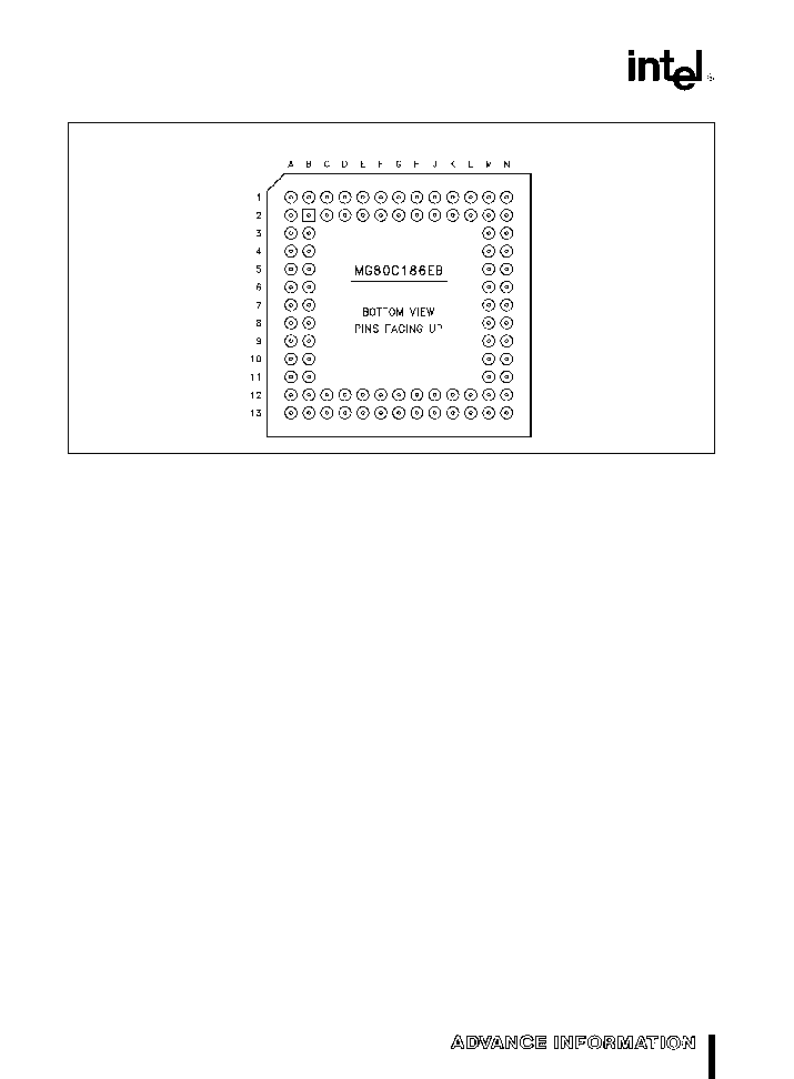
M80C186EB PINOUT
Table 5 lists the M80C186EB pin names with pack-
age location for the 88-Lead Pin Grid Array (PGA)
component
Figure
8
depicts
the
complete
M80C186EB pinout as viewed from the bottom side
of the component
Table 5 MG80C186EB Pin Assignments
PLCC PGA
Name
11
1A
DEN
10
2B
S0
9
1B
S1
8
2C
S2
7
1C
BHE
6
2D
ALE
5
1D
WR
4
2E
RD
3
1E
ERROR
2
2F
V
SS
1
1F
V
CC
84
2G
V
SS
83
1G
A19 ONCE
82
2H
A18
81
1H
A17
80
2J
A16
79
1J
AD15
78
2K
AD7
77
1K
AD14
76
2L
AD6
75
1L
AD13
2M
N C
PLCC PGA
Name
74
1M AD5
73
1N
AD12
72
2N
AD4
71
3M AD11
70
3N
AD3
69
4M AD10
68
4N
AD2
67
5M AD9
66
5N
AD1
65
6M V
SS
64
6N
V
CC
63
7M V
SS
7N
N C
62
8M AD8
61
8N
AD0
60
9M NCS
59
9N
P2 2 BCLK1
58
10M P2 1 TXD1
57
10N P2 0 RXD1
56
11M P2 4 CTS1
55
11N P2 3 SINT1
54
12M P2 5 BLCK0
PLCC
PGA
Name
12N
N C
53
13N
RXD0
52
13M
TXD0
51
12L
CTS0
50
13L
P2 6
49
12K
P2 7
48
13K
T1IN
47
12J
T1OUT
46
13J
T0IN
45
12H
T0OUT
44
13H
CLKOUT
43
12G
V
SS
42
13G
V
CC
41
12F
CLKIN
40
13F
OSCOUT
39
12E
PEREQ
38
13E
RESOUT
37
12D
RESIN
36
13D
PDTMR
35
12C
INT4
34
13C
INT3
33
12B
INT2
PLCC PGA
Name
13B N C
32
13A INT1
31
12A INT0
30
11B UCS
29
11A LCS
28
10B P1 0 GCS0
27
10A P1 1 GCS1
26
9B
P1 2 GCS2
25
9A
P1 3 GCS3
24
8B
P1 4 GCS4
23
8A
V
CC
22
7B
V
SS
21
7A
P1 5 GCS5
20
6B
P1 6 GCS6
19
6A
P1 7 GCS7
18
5B
READY
17
5A
NMI
16
4B
DRT R
15
4A
LOCK
14
3B
TEST BUSY
13
3A
HOLD
12
2A
HLDA
19
M80C186EB
Pin Grid Array
271214 � 6
Figure 8
20
M80C186EB
ELECTRICAL SPECIFICATIONS
Absolute Maximum Ratings
Parameter
Maximum Rating
Storage Temperature
b
65 C to a150 C
Case Temp Under Bias
b
55 C to a125 C
Supply Voltage
with respect to V
SS
b
0 5V to a6 5V
Voltage on other Pins
with respect to V
SS
b
0 5V to V
CC
a
0 5V
NOTICE This data sheet contains information on
products in the sampling and initial production phases
of development It is valid for the devices indicated in
the revision history The specifications are subject to
change without notice
WARNING Stressing the device beyond the ``Absolute
Maximum Ratings'' may cause permanent damage
These are stress ratings only Operation beyond the
``Operating Conditions'' is not recommended and ex-
tended exposure beyond the ``Operating Conditions''
may affect device reliability
OPERATING CONDITIONS
Symbol
Parameter
Min
Max
Units
V
CC
Supply Voltage
4 5
5 5
V
T
F
Input Clock Frequency
M80C186EB-16
0
32
MHz
M80C186EB-13
0
26 08
MHz
M80C186EB-8
0
16
MHz
T
C
Case Temperature Under Bias
b
55
a
125
C
RECOMMENDED CONNECTIONS
Power and ground connections must be made to
multiple V
CC
and V
SS
pins Every M80C186EB-
based circuit board should include separate power
(V
CC
) and ground (V
SS
) planes Every V
CC
pin must
be connected to the power plane and every V
SS
pin
must be connected to the ground plane Pins identi-
fied as ``NC'' must not be connected in the system
Liberal decoupling capacitance should be placed
near the M80C186EB The processor can cause
transient power surges when its output buffers tran-
sition particularly when connected to large capaci-
tive loads
Low inductance capacitors and interconnects are
recommended for best high frequency electrical per-
formance Inductance is reduced by placing the de-
coupling capacitors as close as possible to the
M80C186EB V
CC
and V
SS
package pins
Always connect any unused input to an appropriate
signal level In particular unused interrupt inputs
(INT0 4) should be connected to V
CC
through a pull-
up resistor (in the range of 50 KX) Leave any un-
used output pin or any NC pin unconnected
21
M80C186EB
DC SPECIFICATIONS
Symbol
Parameter
Min
Max
Units
Notes
V
IL
Input Low Voltage
b
0 5
0 3 V
CC
V
(Note 8)
V
IH
Input High Voltage
0 7 V
CC
V
CC
a
0 5
V
V
OL
Output Low Voltage
0 45
V
I
OL
e
3 mA (Min)
V
OH
Output High Voltage
V
CC
b
0 5
V
I
OH
e b
2 mA (MIn)
V
HYR
Input Hysterisis on RESIN
0 50
V
I
LI1
Input Leakage Current for pins
AD15 0 READY HOLD RESIN
TEST NMI INT4 0 T0IN T1IN RXD0
g
15
m
A
0V
s
V
IN
s
V
CC
BCLK0 CTS0 RXD1 BCLK1 CTS1
P2 6 P2 7
I
LI2
Input Leakage Current for Pin CLKIN
g
50
m
A
0V
s
V
IN
s
V
CC
I
I1
Input Current for Pin ERROR
b
7
b
0 275
mA
V
IN
e
0V
I
I2
Input Current for Pin PEREQ
a
0 275
a
7
mA
V
IN
e
V
CC
I
LO
Output Leakage Current
g
15
m
A
0 45
s
V
OUT
s
V
CC
(Notes 2 7)
I
CC
Supply Current Cold (RESET)
M80C186EB-16
90
mA
(Note 3)
M80C186EB-13
73
mA
(Note 3)
M80C186EB-8
45
mA
(Note 3)
I
ID
Supply Current Idle
M80C186EB-16
63
mA
(Note 4)
M80C186EB-13
48
mA
(Note 4)
M80C186EB-8
31
mA
(Note 4)
I
PD
Supply Current Powerdown
M80C186EB-16
100
m
A
(Note 5)
M80C186EB-13
100
m
A
(Note 5)
M80C186EB-8
100
m
A
(Note 5)
CIN
Input Pin Capacitance
0
15
pF
T
F
e
1 MHz
COUT
Output Pin Capacitance
0
15
pF
T
F
e
1 MHz (Note 6)
NOTES
1 These pins have an internal pull-up device that is active while RESIN is low and ONCE Mode is not active Sourcing more
current than specified (on any of these pins) may invoke a factory test mode
2 Tested by outputs being floated by invoking ONCE Mode or by asserting HOLD
3 Measured with the device in RESET and at worst case frequency V
CC
and temperature with ALL outputs loaded as
specified in AC Test Conditions and all floating outputs driven to V
CC
or GND
4 Measured with the device in HALT (IDLE Mode active) and at worst case frequency V
CC
and temperature with ALL
outputs loaded as specified in AC Test Conditions and all floating outputs driven to V
CC
or GND
5 Measured with the device in HALT (Powerdown Mode active) and at worst case frequency V
CC
and temperature with
ALL
outputs loaded as specified in AC Test Conditions and all floating outputs driven to V
CC
or GND
6 Output Capacitance is the capacitive load of a floating output pin
7 OSC out is not tested
8 A19 ONCE A18 16 LOCK are not tested
22
M80C186EB
I
CC
VERSUS FREQUENCY AND VOLTAGE
The current (I
CC
) consumption of the M80C186EB is
essentially composed of two components I
PD
and
I
CCS
I
PD
is the quiescent current that represents internal
device leakage and is measured with all inputs or
floating outputs at GND or V
CC
(no clock applied to
the device) I
PD
is equal to the Powerdown current
and is typically less than 50 mA
I
CCS
is the switching current used to charge and
discharge parasitic device capacitance when chang-
ing logic levels Since I
CCS
is typically much greater
than I
PD
I
PD
can often be ignored when calculating
I
CC
I
CCS
is related to the voltage and frequency at which
the device is operating It is given by the formula
Power e V
c
I e V
2 c
C
DEV
c
f
I e I
CC
e
I
CCS
e
V
c
C
DEV
c
f
Where V e Device operating voltage (V
CC
)
C
DEV
e
Device capacitance
f e Device operating frequency
I
CCS
e
I
CC
e
Device current
Measuring C
DEV
on a device like the M80C186EB
would be difficult Instead C
DEV
is calculated using
the above formula by measuring I
CC
at a known V
CC
and frequency (see Table 11) Using this C
DEV
val-
ue I
CC
can be calculated at any voltage and fre-
quency within the specified operating range
EXAMPLE Calculate the typical I
CC
when operating
at 10 MHz 4 8V
I
CC
e
I
CCS
e
4 8
c
0 583
c
10
28 mA
PDTMR PIN DELAY CALCULATION
The PDTMR pin provides a delay between the as-
sertion of NMI and the enabling of the internal
clocks when exiting Powerdown A delay is required
only when using the on-chip oscillator to allow the
crystal or resonator circuit time to stabilize
NOTE
The PDTMR pin function does not apply when
RESIN is asserted (i e a device reset during Pow-
erdown is similar to a cold reset and RESIN must
remain active until after the oscillator has stabi-
lized)
To calculate the value of capacitor required to pro-
vide a desired delay use the equation
440
c
t e C
PD
(5V 25 C)
Where t e desired delay in seconds
C
PD
e
capacitive load on PDTMR in mi-
crofarads
EXAMPLE To get a delay of 300 ms a capacitor
value of C
PD
e
440
c
(300
c
10
b
6
) e 0 132 mF is
required Round up to standard (available) capaci-
tive values
NOTE
The above equation applies to delay times greater
than 10 ms and will compute the TYPICAL capaci-
tance needed to achieve the desired delay A delay
variance of a50% or b25% can occur due to
temperature
voltage
and device process ex-
tremes In general higher V
CC
and or lower tem-
perature will decrease delay time while lower V
CC
and or higher temperature will increase delay time
Table 11 Device Capacitance (C
DEV
) Values
Parameter
Typ
Max
Units
Notes
C
DEV
(Device in Reset)
0 583
1 02
mA V MHz
1 2
C
DEV
(Device in Idle)
0 408
0 682
mA V MHz
1 2
1 Max C
DEV
is calculated at
b
40 C all floating outputs driven to V
CC
or GND and all
outputs loaded to 50 pF (including CLKOUT and OSCOUT)
2 Typical C
DEV
is calculated at 25 C with all outputs loaded to 50 pF except CLKOUT and
OSCOUT which are not loaded
23
M80C186EB
AC SPECIFICATIONS
AC Characteristics
M80C186EB-16
Symbol
Parameter
Min
Max
Units
Notes
INPUT CLOCK
T
F
CLKIN Frequency
0
32
MHz
1
T
C
CLKIN Period
31 25
%
ns
1
T
CH
CLKIN High Time
10
%
ns
1 2
T
CL
CLKIN Low Time
10
%
ns
1 2
T
CR
CLKIN Rise Time
1
8
ns
1 3 11
T
CF
CLKIN Fall Time
1
8
ns
1 3 11
OUTPUT CLOCK
T
CD
CLKIN to CLKOUT Delay
0
20
ns
1 4
T
CLKOUT Period
2 T
C
ns
1
T
PH
CLKOUT High Time
(T 2) b 5
(T 2) a 5
ns
1
T
PL
CLKOUT Low Time
(T 2) b 5
(T 2) a 5
ns
1
T
PR
CLKOUT Rise Time
6
ns
1 5
T
PF
CLKOUT Fall Time
6
ns
1 5
OUTPUT DELAYS
T
CHOV1
ALE S2 0 DEN DT R BHE
1
22
ns
1 4 6 7
LOCK A19 16
T
CHOV2
GCS0 7 LCS UCS NCS RD WR
1
27
ns
1 4 6 8
T
CLOV1
BHE DEN LOCK RESOUT HLDA
1
22
ns
1 4 6
T0OUT T1OUT A19 16
T
CLOV2
RD WR GCS7 0 LCS UCS
1
27
ns
1 4 6
AD15 0 NCS INTA1 0 S2 0
T
CHOF
RD WR BHE DT R
0
25
ns
1 11
LOCK S2 0 A19 16
T
CLOF
DEN AD15 0
0
25
ns
1 11
SYNCHRONOUS INPUTS
T
CHIS
TEST NMI INT4 0 BCLK1 0
10
ns
1 9
T1 0IN READY CTS1 0 P2 6 P2 7
T
CHIH
TEST NMI INT4 0 BCLK1 0
3
ns
1 9
T1 0IN READY CTS1 0
T
CLIS
AD15 0 READY
10
ns
1 10
T
CLIH
READY AD15 0
3
ns
1 10
T
CLIS
HOLD PEREQ ERROR
10
ns
1 9
T
CLIH
HOLD PEREQ ERROR
3
ns
1 9
NOTES
1 See AC Timing Waveforms for waveforms and definition
2 Measure at V
IH
for high time V
IL
for low time
3 Only required to guarantee I
CC
Maximum limits are bounded by T
C
T
CH
and T
CL
4 Specified for a 50 pF load see Figure 16 for capacitive derating information
5 Specified for a 50 pF load see Figure 17 for rise and fall times outside 50 pF
6 See Figure 17 for rise and fall times
7 T
CHOV1
applies to BHE LOCK and A19 16 only after a HOLD release
8 T
CHOV2
applies to RD and WR only after a HOLD release
9 Setup and Hold are required to guarantee recognition
10 Setup and Hold are required for proper M80C186EB operation
11 Not tested
24
M80C186EB
AC SPECIFICATIONS
AC Characteristics
M80C186EB-13
Symbol
Parameter
Min
Max
Units
Notes
INPUT CLOCK
T
F
CLKIN Frequency
0
26 08
MHz
1
T
C
CLKIN Period
38 34
%
ns
1
T
CH
CLKIN High Time
12
%
ns
1 2
T
CL
CLKIN Low Time
12
%
ns
1 2
T
CR
CLKIN Rise Time
1
8
ns
1 3
T
CF
CLKIN Fall Time
1
8
ns
1 3
OUTPUT CLOCK
T
CD
CLKIN to CLKOUT Delay
0
23
ns
1 4
T
CLKOUT Period
2 T
C
ns
1
T
PH
CLKOUT High Time
(T 2) b 5
(T 2) a 5
ns
1
T
PL
CLKOUT Low Time
(T 2) b 5
(T 2) a 5
ns
1
T
PR
CLKOUT Rise Time
6
ns
1 5
T
PF
CLKOUT Fall Time
6
ns
1 5
OUTPUT DELAYS
T
CHOV1
ALE S2 0 DEN DT R BHE
1
25
ns
1 4 6 7
LOCK A19 16
T
CHOV2
GCS0 7 LCS UCS NCS RD WR
1
30
ns
1 4 6 8
T
CLOV1
BHE DEN LOCK RESOUT HLDA
1
25
ns
1 4 6
T0OUT T1OUT A19 16
T
CLOV2
RD WR GCS7 0 LCS UCS
1
30
ns
1 4 6
AD15 0 NCS INTA1 0 S2 0
T
CHOF
RD WR BHE DT R
0
25
ns
1 11
LOCK S2 0 A19 16
T
CLOF
DEN AD15 0
0
25
ns
1 11
SYNCHRONOUS INPUTS
T
CHIS
TEST NMI INT4 0 BCLK1 0
10
ns
1 9
T1 0IN READY CTS1 0 P2 6 P2 7
T
CHIH
TEST NMI INT4 0 BCLK1 0
3
ns
1 9
T1 0IN READY CTS1 0
T
CLIS
AD15 0 READY
10
ns
1 10
T
CLIH
READY AD15 0
3
ns
1 10
T
CLIS
HOLD PEREQ ERROR
10
ns
1 9
T
CLIH
HOLD PEREQ ERROR
3
ns
1 9
NOTES
1 See AC Timing Waveforms for waveforms and definition
2 Measure at V
IH
for high time V
IL
for low time
3 Only required to guarantee I
CC
Maximum limits are bounded by T
C
T
CH
and T
CL
4 Specified for a 50 pF load see Figure 16 for capacitive derating information
5 Specified for a 50 pF load see Figure 17 for rise and fall times outside 50 pF
6 See Figure 17 for rise and fall times
7 T
CHOV1
applies to BHE LOCK and A19 16 only after a HOLD release
8 T
CHOV2
applies to RD and WR only after a HOLD release
9 Setup and Hold are required to guarantee recognition
10 Setup and Hold are required for proper M80C186EB operation
11 Not tested
25

M80C186EB
AC Characteristics
M80C186EB-8
Symbol
Parameter
Min
Max
Units
Notes
INPUT CLOCK
T
F
CLKIN Frequency
0
16
MHz
1
T
C
CLKIN Period
62 5
%
ns
1
T
CH
CLKIN High Time
15
%
ns
1 2
T
CL
CLKIN Low Time
15
%
ns
1 2
T
CR
CLKIN Rise Time
1
8
ns
1 3
T
CF
CLKIN Fall Time
1
8
ns
1 3
OUTPUT CLOCK
T
CD
CLKIN to CLKOUT Delay
0
27
ns
1 4
T
CLKOUT Period
2 T
C
ns
1
T
PH
CLKOUT High Time
(T 2) b 5
(T 2) a 5
ns
1
T
PL
CLKOUT Low Time
(T 2) b 5
(T 2) a 5
ns
1
T
PR
CLKOUT Rise Time
6
ns
1 5
T
PF
CLKOUT Fall Time
6
ns
1 5
OUTPUT DELAYS
T
CHOV1
ALE S2 0 DEN DT R BHE
1
30
ns
1 4 6 7
LOCK A19 16
T
CHOV2
GCS0 7 LCS UCS NCS RD WR
1
35
ns
1 4 6 8
T
CLOV1
BHE DEN LOCK RESOUT HLDA
1
30
ns
1 4 6
T0OUT T1OUT A19 16
T
CLOV2
RD WR GCS7 0 LCS UCS
1
35
ns
1 4 6
AD15 0 NCS INTA1 0 S2 0
T
CHOF
RD WR BHE DT R
0
30
ns
1 11
LOCK S2 0 A19 16
T
CLOF
DEN AD15 0
0
35
ns
1 11
SYNCHRONOUS INPUTS
T
CHIS
TEST NMI INT4 0 BCLK1 0
10
ns
1 9
T1 0IN READY CTS1 0 P2 6 P2 7
T
CHIH
TEST NMI INT4 0 BCLK1 0
3
ns
1 9
T1 0IN READY CTS1 0
T
CLIS
AD15 0 READY
10
ns
1 10
T
CLIH
READY AD15 0
3
ns
1 10
T
CLIS
HOLD PEREQ ERROR
10
ns
1 9
T
CLIH
HOLD PEREQ ERROR
3
ns
1 9
NOTES
1 See AC Timing Waveforms for waveforms and definition
2 Measure at V
IH
for high time V
IL
for low time
3 Only required to guarantee I
CC
Maximum limits are bounded by T
C
T
CH
and T
CL
4 Specified for a 50 pF load see Figure 16 for capacitive derating information
5 Specified for a 50 pF load see Figure 17 for rise and fall times outside 50 pF
6 See Figure 17 for rise and fall times
7 T
CHOV1
applies to BHE LOCK and A19 16 only after a HOLD release
8 T
CHOV2
applies to RD and WR only after a HOLD release
9 Setup and Hold are required to guarantee recognition
10 Setup and Hold are required for proper M80C186EB operation
11 Not tested
26

M80C186EB
Relative Timings (M80C186EB-16 -13 -8)
Symbol
Parameter
Min
Max
Unit
Notes
RELATIVE TIMINGS
T
LHLL
ALE Rising to ALE Falling
T b 15
ns
T
AVLL
Address Valid to ALE Falling
T b 10
ns
T
PLLL
Chip Selects Valid to ALE Falling
T b 10
ns
1
T
LLAX
Address Hold from ALE Falling
T b 10
ns
T
LLWL
ALE Falling to WR Falling
T b 15
ns
1
T
LLRL
ALE Falling to RD Falling
T b 15
ns
1
T
WHLH
WR Rising to ALE Rising
T b 10
ns
1
T
AFRL
Address Float to RD Falling
0
ns
T
RLRH
RD Falling to RD Rising
(2 T) b 5
ns
2
T
WLWH
WR Falling to WR Rising
(2 T) b 5
ns
2
T
RHAV
RD Rising to Address Active
T b 15
ns
T
WHDX
Output Data Hold after WR Rising
T b 15
ns
T
WHPH
WR Rising to Chip Select Rising
T b 10
ns
1
T
RHPH
RD Rising to Chip Select Rising
T b 10
ns
1
T
PHPL
CS Inactive to CS Active
T b 10
ns
1
T
OVRH
ONCE Active to RESIN Rising
T
ns
3
T
RHOX
ONCE Hold from RESIN Rising
T
ns
3
NOTES
1 Assumes equal loading on both pins
2 Can be extended using wait states
3 Not tested
27
M80C186EB
Serial Port Mode 0 Timings (M80C186EB-16 -13 -8)
Symbol
Parameter
Min
Max
Unit Notes
T
XLXL
TXD Clock Period
T (n a 1)
ns
1 2
T
XLXH
TXD Clock Low to Clock High (n
l
1)
2T b 35
2T a 35
ns
1
T
XLXH
TXD Clock Low to Clock High (n e 1)
T b 35
T a 35
ns
1
T
XHXL
TXD Clock High to Clock Low (n
l
1)
(n b 1) T b 35 (n b 1) T a 35
ns
1 2
T
XHXL
TXD Clock High to Clock Low (n e 1)
T b 35
T a 35
ns
1
T
QVXH
RXD Output Data Setup to TXD Clock High (n
l
1)
(n b 1) T b 35
ns
1 2
T
QVXH
RXD Output Data Setup to TXD Clock High (n e 1)
T b 35
ns
1
T
XHQX
RXD Output Data Hold after TXD Clock High (n
l
1)
2T b 35
ns
1
T
XHQX
RXD Output Data Hold after TXD Clock High (n e 1)
T b 35
ns
1
T
XHQZ
RXD Output Data Float after Last TXD Clock High
T a 20
ns
1 3
T
DVXH
RXD Input Data Setup to TXD Clock High
T a 20
ns
1
T
XHDX
RXD Input Data Hold after TXD Clock High
0
ns
1 3
NOTES
1 See Figure 14 for waveforms
2 n is the value of the BxCMP register ignoring the ICLK Bit (i e ICLK
e
0)
3 Guaranteed not tested
28

M80C186EB
AC TEST CONDITIONS
The AC specifications are tested with the 50 pF load
shown in Figure 9 See the Derating Curves section
to see how timings vary with load capacitance
Specifications are measured at the V
CC
2 crossing
point unless otherwise specified See AC Timing
Waveforms for AC specification definitions test
pins and illustrations
271214 � 7
C
L
e
50 pF for all signals
Figure 9 AC Test Load
AC TIMING WAVEFORMS
271214 � 8
Figure 10 Input and Output Clock Waveform
29
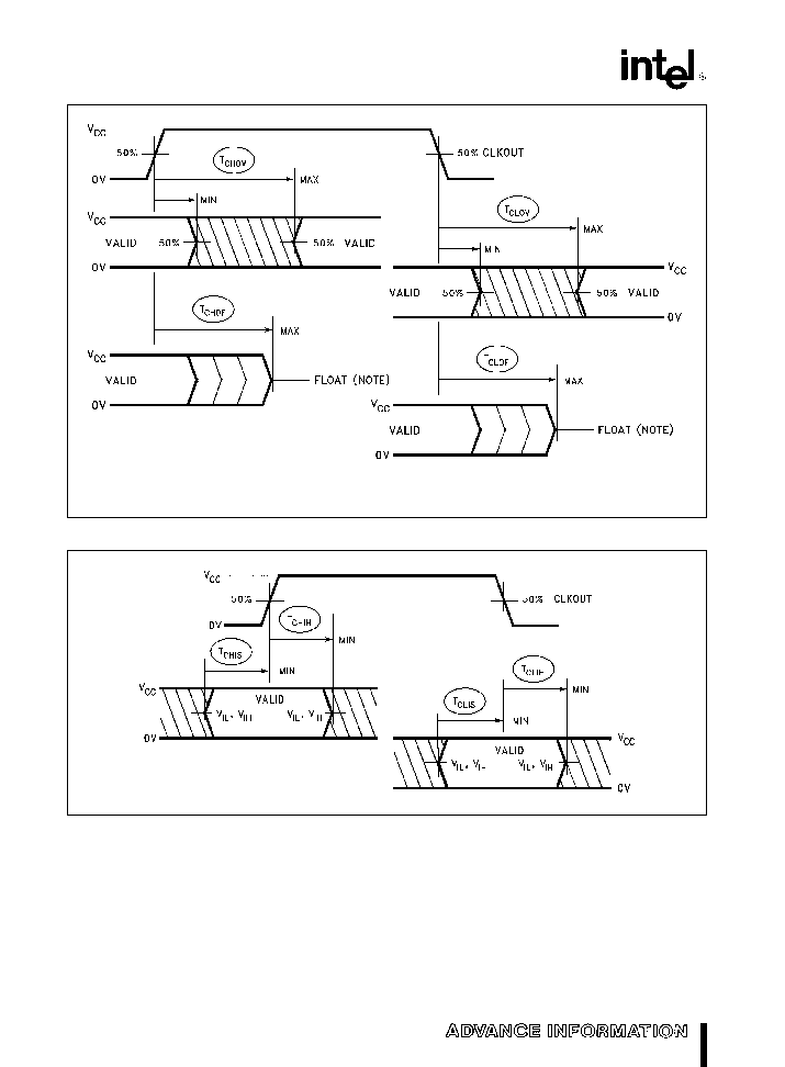
M80C186EB
271214 � 9
NOTE
20% V
CC
k
Float
k
80% V
CC
Figure 11 Output Delay and Float Waveform
271214 � 10
Figure 12 Input Setup and Hold
30
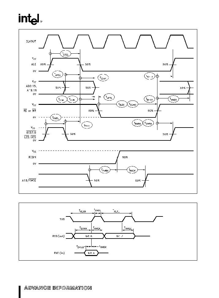
M80C186EB
271214 � 11
Figure 13 Relative Signal Waveform
271214 � 12
Figure 14 Serial Port Mode 0 Waveform
31
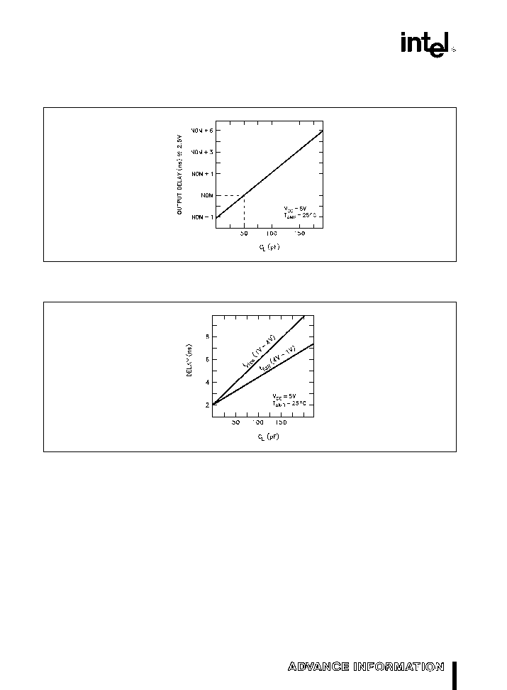
M80C186EB
DERATING CURVES
TYPICAL OUTPUT DELAY VARIATIONS VERSUS LOAD CAPACITANCE
271214 � 13
Figure 15
TYPICAL RISE AND FALL VARIATIONS VERSUS LOAD CAPACITANCE
271214 � 14
Figure 16
32

M80C186EB
RESET
The M80C186EB will perform a reset operation any
time the RESIN pin active The RESIN pin is actually
synchronized before it is presented internally which
means that the clock must be operating before a
reset can take effect From a power-on state RESIN
must be held active (low) in order to guarantee cor-
rect initialization of the M80C186EB Failure to pro-
vide RESIN while the device is powering up will
result in unspecified operation of the device
Figure 17 shows the correct reset sequence when
first applying power to the M80C186EB An external
clock connected to CLKIN must not exceed the V
CC
threshold being applied to the M80C186EB This is
normally not a problem if the clock driver is supplied
with the same V
CC
that supplies the M80C186EB
When attaching a crystal to the device RESIN must
remain active until both V
CC
and CLKOUT are stable
(the length of time is application specific and de-
pends on the startup characteristics of the crystal
circuit) The RESIN pin is designed to operate cor-
rectly using an RC reset circuit but the designer
must ensure that the ramp time for V
CC
is not so
long that RESIN is never really sampled at a logic
low level when V
CC
reaches minimum operating
conditions
Figure 18 shows the timing sequence when RESIN
is applied after V
CC
is stable and the device has
been operating Note that a reset will terminate all
activity and return the M80C186EB to a known oper-
ating state Any bus operation that is in progress at
the time RESIN is asserted will terminate immediate-
ly (note that most control signals will be driven to
their inactive state first before floating)
While RESIN is active bus signals LOCK A19
ONCE and A18 16 are configured as inputs and
weakly held high by internal pullup transistors Only
19 ONCE can be overdriven to a low and is used to
enable ONCE Mode Forcing LOCK or A18 16 low at
any time while RESIN is low is prohibited and will
cause unspecified device operation
33

M80C186EB
COLD RESET WAVEFORMS
Figure 17
271214
�
1
5
NOTE
CLKOUT
synchronization
occurs
on
the
rising
edge
of
RESIN
I
f
RESIN
is
sampled
high
while
CLKOUT
is
high
(solid
line)
then
CLKOUT
will
remain
low
for
two
CLKIN
periods
If
RESIN
is
sampled
high
while
CLKOUT
is
low
(dashed
line)
then
CLKOUT
will
not
be
affected
34

M80C186EB
WARM RESET WAVEFORMS
Figure 18
271214
�
1
6
35

M80C186EB
BUS CYCLE WAVEFORMS
Figures 19 through 25 present the various bus cy-
cles that are generated by the M80C186EB What is
shown in the figure is the relationship of the various
bus signals to CLKOUT These figures along with
the information present in AC Specifications allow
the user to determine all the critical timing analysis
needed for a given application
Figure 19 shows the M80C186EB bus state diagram
A typical bus cycle will consist of four consecutive
states labeled T1 T2 T3 and T4 A TI state exists
when no bus cycle is pending A TI state can occur if
the pre-fetch queue is full the BIU is waiting for the
completion of an effective address calculation or
the BIU is told to wait for a pending EU bus opera-
tion The latter case will occur most often during the
sequencing of an interrupt acknowledge or during
the execution of numerics escape instructions
Aside from TI states multiple T3 states can occur
during a bus cycle if READY is not returned in time
(or the CSU has been programmed to automatically
insert wait-states) A T3 state will be followed by ei-
ther a T4 state (if a bus cycle is pending) or a TI
state (if no bus cycle is pending) Only multiple T3 or
TI states can exist (i e there is no way to extend the
T1 T2 or T4 states)
Figures 20 and 21 present a typical bus read and
write operation respectively Bus read operations in-
clude memory I O instruction fetch and refresh
bus cycles Bus write operations include memory
and I O bus cycles The only variation among the
different bus cycles would be the range of address
generated and the state of the status signals
The Halt bus cycle is shown in Figure 22 Note that
the condition of the AD15 0 pin can be either floating
or driving depending on the operation of the bus cy-
cle that preceded the Halt The pins will float if the
previous bus cycle was a read otherwise they will
drive None of the control signals (e g
RD WR
DEN etc ) will be activated however
Figure 23 shows the sequence of bus cycles run
when an interrupt is acknowledged and the ICU has
been programmed for Cascade Mode Note the ad-
dress information is not valid for the two bus cycles
run however also note that RD and WR are not
generated Vector information needs to be returned
during the second bus cycle
Figures 24 and 25 present the operation of bus
HOLD Figure 24 shows how bus HOLD is entered
and exited under normal operating conditions Fig-
ure 25 shows the effect specific bus signals have
when a refresh bus cycle request has been generat-
ed and the bus is currently unavailable due to a bus
HOLD
The effects of READY on bus operation is shown in
Figure 26 READY is useful in extending the bus cy-
cle to meet the various access requirements for
memory and peripheral devices in the system Addi-
tional T3 states added to the bus cycle have been
appropriately labeled Tw
271214 � 17
Figure 19 M80C186EB Bus States
36
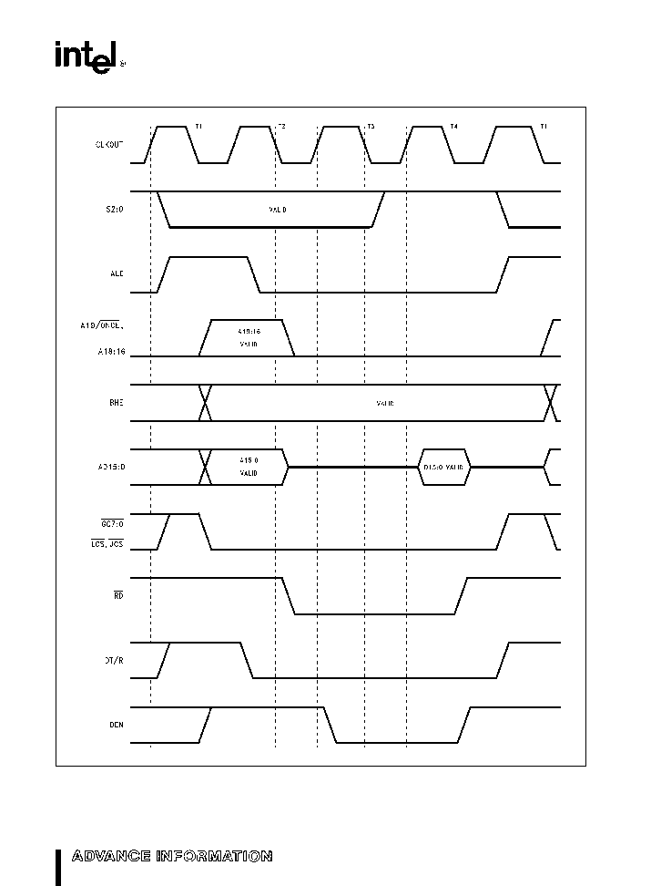
M80C186EB
MEMORY READ I O READ INSTRUCTION FETCH AND REFRESH WAVEFORM
271214 � 18
Figure 20
37
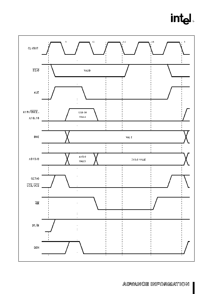
M80C186EB
MEMORY WRITE AND I O WRITE CYCLE WAVEFORM
271214 � 19
Figure 21
38

M80C186EB
HALT CYCLE WAVEFORM
271214 � 20
NOTE
The address driven is typically the location of the next instruction prefetch Under a majority of instruction sequences the
AD15 0 bus will float while the A19 16 bus remains driven and all bus control signals are driven to their inactive state
Figure 22
39
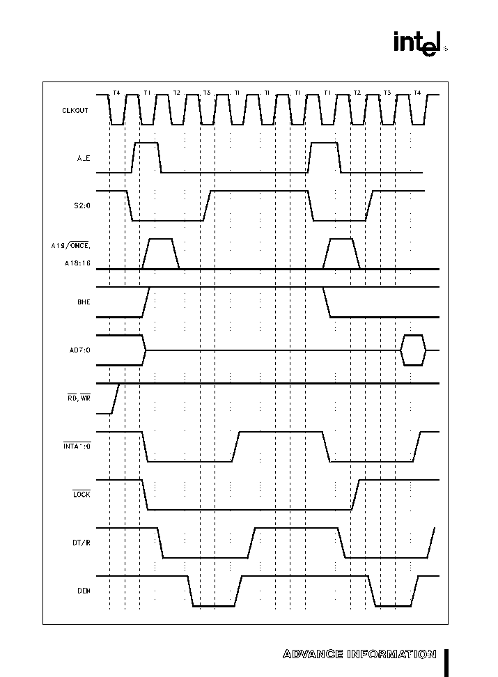
M80C186EB
CASCADE MODE INTERRUPT ACKNOWLEDGE CYCLE WAVEFORM
271214 � 21
Figure 23
40
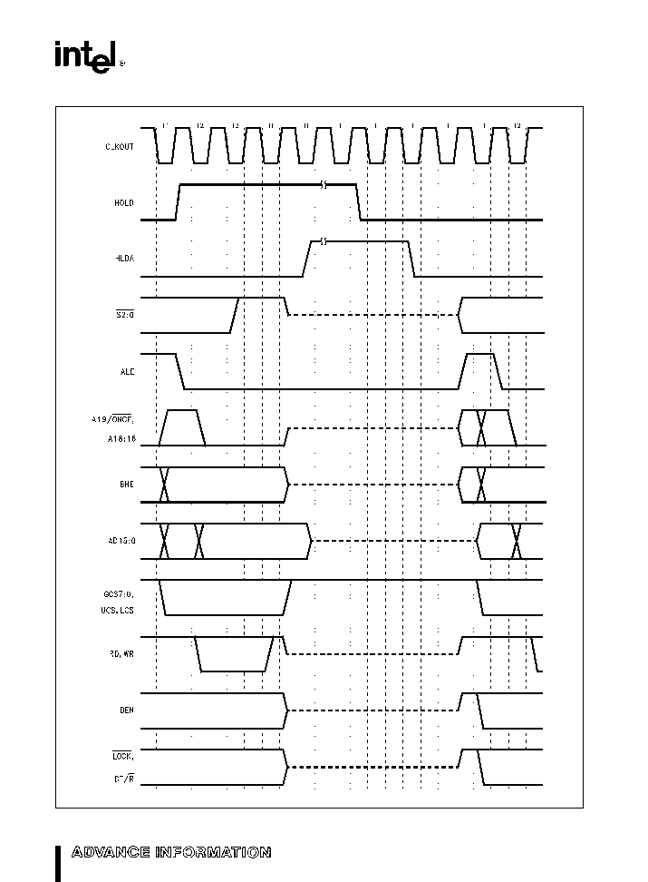
M80C186EB
HOLD HLDA CYCLE WAVEFORMS
271214 � 22
Figure 24
41
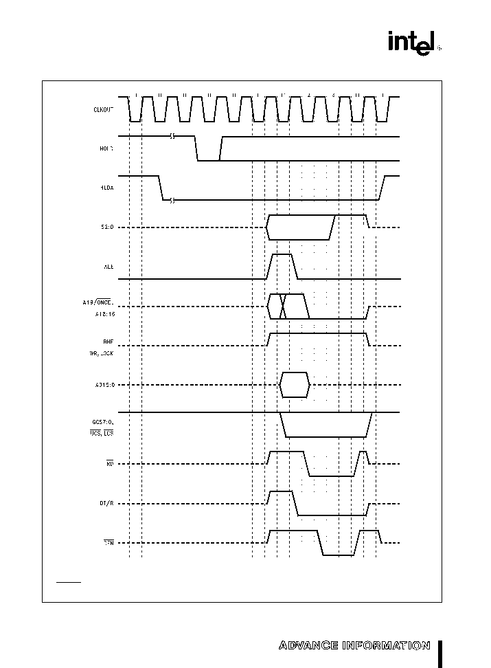
M80C186EB
REFRESH DURING HLDA CYCLE WAVEFORM
271214 � 23
NOTES
1 READY must be low by either edge to cause a wait state
2 Lighter lines indicate READ cycles darker lines indicate WRITE cycles
Figure 25
42

M80C186EB
READY CYCLE WAVEFORM
271214 � 24
NOTES
1 READY must be low by either edge to cause a wait state
2 Lighter lines indicate READ cycles darker lines indicate WRITE cycles
Figure 26
43

M80C186EB
REGISTER BIT SUMMARY
Figures 27 through 34 present the bit definition of
each register that is active (not reserved) in the Pe-
ripheral Control Block (PCB) Each register can be
thought to occupy one word (16-bits) of either mem-
ory or I O space although not all bits in the register
necessarily have a function A register bit is not
guaranteed to return a specific logic value if an ``X''
appears for the bit definition (i e if a zero was writ-
ten to the register bit it may not be returned as a
zero when read) Furthermore a 0 must be written to
any bit that is indicated by an ``X'' to ensure compati-
bility with future products or potential product chang-
es
Not all defined register bits can be read and or
written
although most registers are read write
Some registers like the P1DIR register exist but do
not have any effect on the operation of the
M80C186EB For example the Port1 pins are output
only and cannot be changed by programming the
P1DIR register However the P1DIR register can still
be read and written
which allows the P1DIR regis-
ter to be used as a temporary 8-bit data register
Reads and writes to any of the PCB registers will
cause a bus cycle to be run externally however
none of the chip selects will go active (even if they
overlap the PCB address range) Data read back
from the AD15 0 bus is ignored and all cycles will
take zero wait states (except accesses to the Timer
Counter registers which take one wait state due to
internal synchronization)
Figures 27 and 28 present the registers associated
with the Interrupt Control Unit (ICU) A write to the
MASK (08H) register will also effect the correspond-
ing MSK bit in each of the control registers (e g
setting the TMR bit in the MASK register will also set
the MSK bit in the TMRCON register)
The Timer Counter Unit registers are presented in
Figure 29 The compare and count registers are not
initialized after reset and must be set correctly dur-
ing initialization to ensure the timer operates correct-
ly the first time it is enabled
Figure 30 presents the I O Port Unit (IPU) registers
Only PD6 and PD7 or of the P2DIR register have any
effect on the direction of the port pins (P2 6 and
P2 7 respectively) The unused bits of P2DIR and all
the bits of P1DIR can be thought of having latches
that can be read and written The two PxLTCH regis-
ters have all 8-bits implemented however only
those port pins which can function as outputs actual-
ly use the value programmed into the latch Other-
wise (like the P1DIR register) the registers can be
thought of being an 8-bit data register
Figure 31 presents the register bit definitions of the
Serial Communications Unit (SCU) The transmit and
receive buffer registers are both readable and write-
able Note that a read from SxSTS register will clear
all of the status information (except for CTS which
actually is derived from the pin itself)
The Chip-Select Unit (CSU) registers are presented
in Figure 32 and the Refresh Control Unit (RCU) reg-
isters are presented in Figure 33 The RFADDR reg-
ister will indicate the current refresh address when
read and a write to the register will change the next
refresh address generated
Figure 34 presents the PWRCON register and
STEPID register The STEPID register contains a
stepping identifier that may or may not change any
time there is a change to the M80C186EB silicon
die The STEPID is for Intel use and can change at
any time
44

M80C186EB
271214 � 25
Figure 27 Interrupt Control Unit Registers
271214 � 26
Figure 28 Interrupt Control Unit Registers
45
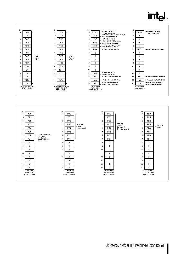
M80C186EB
271214 � 27
Figure 29 Timer Control Unit Registers
271214 � 28
Figure 30 I O Port Unit Registers
46
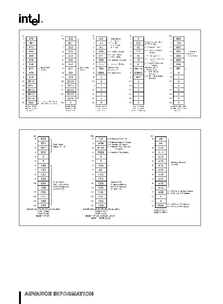
M80C186EB
271214 � 29
Figure 31 Serial Communications Unit Registers
271214 � 30
Figure 32 Chip-Select Unit Registers
47
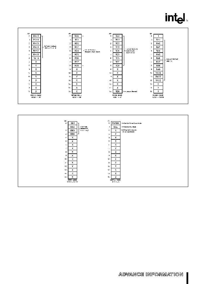
M80C186EB
271214 � 31
Figure 33 Refresh Control Unit Registers
271214 � 32
Figure 34 Power Management Unit Registers
M80C186EB EXECUTION TIMINGS
A determination of M80C186EB program execution
timing must consider the bus cycles necessary to
prefetch instructions as well as the number of exe-
cution unit cycles necessary to execute instructions
The following instruction timings represent the mini-
mum
execution time in clock cycles for each instruc-
tion The timings given are based on the following
assumptions
The opcode along with any data or displacement
required for execution of a particular instruction
has been prefetched and resides in the queue at
the time it is needed
No wait states or bus HOLDs occur
All word-data is located on even-address bound-
aries
All jumps and calls include the time required to fetch
the opcode of the next instruction at the destination
address
All instructions which involve memory accesses can
require one or two additional clocks above the mini-
mum timings shown due to the asynchronous hand-
shake between the bus interface unit (BIU) and exe-
cution unit
With a 16-bit BIU the M80C186EB has sufficient bus
performance to ensure that an adequate number of
prefetched bytes will reside in the queue most of the
time Therefore actual program execution time will
not be substantially greater than that derived from
adding the instruction timings shown
48
M80C186EB
INSTRUCTION SET SUMMARY
Function
Format
Clock
Comments
Cycles
DATA TRANSFER
MOV e Move
Register to Register Memory
1 0 0 0 1 0 0 w
mod reg r m
2 12
Register memory to register
1 0 0 0 1 0 1 w
mod reg r m
2 9
Immediate to register memory
1 1 0 0 0 1 1 w
mod 000 r m
data
data if we1
12 � 13
8 16-bit
Immediate to register
1 0 1 1 w reg
data
data if we1
3 � 4
8 16-bit
Memory to accumulator
1 0 1 0 0 0 0 w
addr-low
addr-high
8
Accumulator to memory
1 0 1 0 0 0 1 w
addr-low
addr-high
9
Register memory to segment register
1 0 0 0 1 1 1 0
mod 0 reg r m
2 9
Segment register to register memory
1 0 0 0 1 1 0 0
mod 0 reg r m
2 11
PUSH e Push
Memory
1 1 1 1 1 1 1 1
mod 1 1 0 r m
16
Register
0 1 0 1 0 reg
10
Segment register
0 0 0 reg 1 1 0
9
Immediate
0 1 1 0 1 0 s 0
data
data if se0
10
PUSHA e Push All
0 1 1 0 0 0 0 0
36
POP e Pop
Memory
1 0 0 0 1 1 1 1
mod 0 0 0 r m
20
Register
0 1 0 1 1 reg
10
Segment register
0 0 0 reg 1 1 1
(reg
i
01)
8
POPA e Pop All
0 1 1 0 0 0 0 1
51
XCHG e Exchange
Register memory with register
1 0 0 0 0 1 1 w
mod reg r m
4 17
Register with accumulator
1 0 0 1 0 reg
3
IN e Input from
Fixed port
1 1 1 0 0 1 0 w
port
10
Variable port
1 1 1 0 1 1 0 w
8
OUT e Output to
Fixed port
1 1 1 0 0 1 1 w
port
9
Variable port
1 1 1 0 1 1 1 w
7
XLAT e
Translate byte to AL
1 1 0 1 0 1 1 1
11
LEA e
Load EA to register
1 0 0 0 1 1 0 1
mod reg r m
6
LDS e
Load pointer to DS
1 1 0 0 0 1 0 1
mod reg r m
(mod
i
11)
18
LES e
Load pointer to ES
1 1 0 0 0 1 0 0
mod reg r m
(mod
i
11)
18
LAHF e
Load AH with flags
1 0 0 1 1 1 1 1
2
SAHF e
Store AH into flags
1 0 0 1 1 1 1 0
3
PUSHF e
Push flags
1 0 0 1 1 1 0 0
9
POPF e
Pop flags
1 0 0 1 1 1 0 1
8
Shaded areas indicate instructions not available in M8086 M8088 microsystems
49
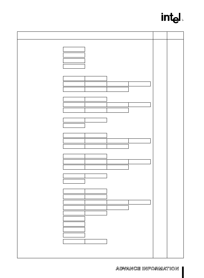
M80C186EB
INSTRUCTION SET SUMMARY
(Continued)
Function
Format
Clock
Comments
Cycles
DATA TRANSFER
(Continued)
SEGMENT e Segment Override
CS
0 0 1 0 1 1 1 0
2
SS
0 0 1 1 0 1 1 0
2
DS
0 0 1 1 1 1 1 0
2
ES
0 0 1 0 0 1 1 0
2
ARITHMETIC
ADD e Add
Reg memory with register to either
0 0 0 0 0 0 d w
mod reg r m
3 10
Immediate to register memory
1 0 0 0 0 0 s w
mod 0 0 0 r m
data
data if s we01
4 16
Immediate to accumulator
0 0 0 0 0 1 0 w
data
data if we1
3 4
8 16-bit
ADC e Add with carry
Reg memory with register to either
0 0 0 1 0 0 d w
mod reg r m
3 10
Immediate to register memory
1 0 0 0 0 0 s w
mod 0 1 0 r m
data
data if s we01
4 16
Immediate to accumulator
0 0 0 1 0 1 0 w
data
data if we1
3 4
8 16-bit
INC e Increment
Register memory
1 1 1 1 1 1 1 w
mod 0 0 0 r m
3 15
Register
0 1 0 0 0 reg
3
SUB e Subtract
Reg memory and register to either
0 0 1 0 1 0 d w
mod reg r m
3 10
Immediate from register memory
1 0 0 0 0 0 s w
mod 1 0 1 r m
data
data if s we01
4 16
Immediate from accumulator
0 0 1 0 1 1 0 w
data
data if we1
3 4
8 16-bit
SBB e Subtract with borrow
Reg memory and register to either
0 0 0 1 1 0 d w
mod reg r m
3 10
Immediate from register memory
1 0 0 0 0 0 s w
mod 0 1 1 r m
data
data if s we01
4 16
Immediate from accumulator
0 0 0 1 1 1 0 w
data
data if we1
3 4
8 16-bit
DEC e Decrement
Register memory
1 1 1 1 1 1 1 w
mod 0 0 1 r m
3 15
Register
0 1 0 0 1 reg
3
CMP e Compare
Register memory with register
0 0 1 1 1 0 1 w
mod reg r m
3 10
Register with register memory
0 0 1 1 1 0 0 w
mod reg r m
3 10
Immediate with register memory
1 0 0 0 0 0 s w
mod 1 1 1 r m
data
data if s we01
3 10
Immediate with accumulator
0 0 1 1 1 1 0 w
data
data if we1
3 4
8 16-bit
NEG e
Change sign register memory
1 1 1 1 0 1 1 w
mod 0 1 1 r m
3 10
AAA e
ASCII adjust for add
0 0 1 1 0 1 1 1
8
DAA e
Decimal adjust for add
0 0 1 0 0 1 1 1
4
AAS e
ASCII adjust for subtract
0 0 1 1 1 1 1 1
7
DAS e
Decimal adjust for subtract
0 0 1 0 1 1 1 1
4
MUL e
Multiply (unsigned)
1 1 1 1 0 1 1 w
mod 100 r m
Register-Byte
26 � 28
Register-Word
35 � 37
Memory-Byte
32 � 34
Memory-Word
41 � 43
Shaded areas indicate instructions not available in M8086 M8088 microsystems
50
M80C186EB
INSTRUCTION SET SUMMARY
(Continued)
Function
Format
Clock
Comments
Cycles
ARITHMETIC
(Continued)
IMUL e
Integer multiply (signed)
1 1 1 1 0 1 1 w
mod 1 0 1 r m
Register-Byte
25 � 28
Register-Word
34 � 37
Memory-Byte
31 � 34
Memory-Word
40 � 43
IMUL e
Integer Immediate multiply
0 1 1 0 1 0 s 1
mod reg r m
data
data if se0
22 � 25
(signed)
29 � 32
DIV e
Divide (unsigned)
1 1 1 1 0 1 1 w
mod 1 1 0 r m
Register-Byte
29
Register-Word
38
Memory-Byte
35
Memory-Word
44
IDIV e
Integer divide (signed)
1 1 1 1 0 1 1 w
mod 1 1 1 r m
Register-Byte
44 � 52
Register-Word
53 � 61
Memory-Byte
50 � 58
Memory-Word
59 � 67
AAM e
ASCII adjust for multiply
1 1 0 1 0 1 0 0
0 0 0 0 1 0 1 0
19
AAD e
ASCII adjust for divide
1 1 0 1 0 1 0 1
0 0 0 0 1 0 1 0
15
CBW e
Convert byte to word
1 0 0 1 1 0 0 0
2
CWD e
Convert word to double word
1 0 0 1 1 0 0 1
4
LOGIC
Shift Rotate Instructions
Register Memory by 1
1 1 0 1 0 0 0 w
mod TTT r m
2 15
Register Memory by CL
1 1 0 1 0 0 1 w
mod TTT r m
5an 17an
Register Memory by Count
1 1 0 0 0 0 0 w
mod TTT r m
count
5an 17an
TTT Instruction
0 0 0
ROL
0 0 1
ROR
0 1 0
RCL
0 1 1
RCR
1 0 0
SHL SAL
1 0 1
SHR
1 1 1
SAR
AND e And
Reg memory and register to either
0 0 1 0 0 0 d w
mod reg r m
3 10
Immediate to register memory
1 0 0 0 0 0 0 w
mod 1 0 0 r m
data
data if we1
4 16
Immediate to accumulator
0 0 1 0 0 1 0 w
data
data if we1
3 4
8 16-bit
TESTeAnd function to flags no result
Register memory and register
1 0 0 0 0 1 0 w
mod reg r m
3 10
Immediate data and register memory
1 1 1 1 0 1 1 w
mod 0 0 0 r m
data
data if we1
4 10
Immediate data and accumulator
1 0 1 0 1 0 0 w
data
data if we1
3 4
8 16-bit
OReOr
Reg memory and register to either
0 0 0 0 1 0 d w
mod reg r m
3 10
Immediate to register memory
1 0 0 0 0 0 0 w
mod 0 0 1 r m
data
data if we1
4 16
Immediate to accumulator
0 0 0 0 1 1 0 w
data
data if we1
3 4
8 16-bit
Shaded areas indicate instructions not available in M8086 M8088 microsystems
51
M80C186EB
INSTRUCTION SET SUMMARY
(Continued)
Function
Format
Clock
Comments
Cycles
LOGIC
(Continued)
XOR e Exclusive or
Reg memory and register to either
0 0 1 1 0 0 d w
mod reg r m
3 10
Immediate to register memory
1 0 0 0 0 0 0 w
mod 1 1 0 r m
data
data if we1
4 16
Immediate to accumulator
0 0 1 1 0 1 0 w
data
data if we1
3 4
8 16-bit
NOT e
Invert register memory
1 1 1 1 0 1 1 w
mod 0 1 0 r m
3 10
STRING MANIPULATION
MOVS e
Move byte word
1 0 1 0 0 1 0 w
14
CMPS e
Compare byte word
1 0 1 0 0 1 1 w
22
SCAS e
Scan byte word
1 0 1 0 1 1 1 w
15
LODS e
Load byte wd to AL AX
1 0 1 0 1 1 0 w
12
STOS e
Store byte wd from AL AX
1 0 1 0 1 0 1 w
10
INS e
Input byte wd from DX port
0 1 1 0 1 1 0 w
14
OUTS e
Output byte wd to DX port
0 1 1 0 1 1 1 w
14
Repeated by count in CX (REP REPE REPZ REPNE REPNZ)
MOVS e
Move string
1 1 1 1 0 0 1 0
1 0 1 0 0 1 0 w
8a8n
CMPS e
Compare string
1 1 1 1 0 0 1 z
1 0 1 0 0 1 1 w
5a22n
SCAS e
Scan string
1 1 1 1 0 0 1 z
1 0 1 0 1 1 1 w
5a15n
LODS e
Load string
1 1 1 1 0 0 1 0
1 0 1 0 1 1 0 w
6a11n
STOS e
Store string
1 1 1 1 0 0 1 0
1 0 1 0 1 0 1 w
6a9n
INS e
Input string
1 1 1 1 0 0 1 0
0 1 1 0 1 1 0 w
8a8n
OUTS e
Output string
1 1 1 1 0 0 1 0
0 1 1 0 1 1 1 w
8a8n
CONTROL TRANSFER
CALL e Call
Direct within segment
1 1 1 0 1 0 0 0
disp-low
disp-high
15
Register memory
1 1 1 1 1 1 1 1
mod 0 1 0 r m
13 19
indirect within segment
Direct intersegment
1 0 0 1 1 0 1 0
segment offset
23
segment selector
Indirect intersegment
1 1 1 1 1 1 1 1
mod 0 1 1 r m
(mod
i
11)
38
JMP e Unconditional jump
Short long
1 1 1 0 1 0 1 1
disp-low
14
Direct within segment
1 1 1 0 1 0 0 1
disp-low
disp-high
14
Register memory
1 1 1 1 1 1 1 1
mod 1 0 0 r m
11 17
indirect within segment
Direct intersegment
1 1 1 0 1 0 1 0
segment offset
14
segment selector
Indirect intersegment
1 1 1 1 1 1 1 1
mod 1 0 1 r m
(mod
i
11)
26
Shaded areas indicate instructions not available in M8086 M8088 microsystems
52
M80C186EB
INSTRUCTION SET SUMMARY
(Continued)
Function
Format
Clock
Comments
Cycles
CONTROL TRANSFER
(Continued)
RET e Return from CALL
Within segment
1 1 0 0 0 0 1 1
16
Within seg adding immed to SP
1 1 0 0 0 0 1 0
data-low
data-high
18
Intersegment
1 1 0 0 1 0 1 1
22
Intersegment adding immediate to SP
1 1 0 0 1 0 1 0
data-low
data-high
25
JE JZ e
Jump on equal zero
0 1 1 1 0 1 0 0
disp
4 13
JMP not
JL JNGE e
Jump on less not greater or equal
0 1 1 1 1 1 0 0
disp
4 13
taken JMP
JLE JNG e
Jump on less or equal not greater
0 1 1 1 1 1 1 0
disp
4 13
taken
JB JNAE e
Jump on below not above or equal
0 1 1 1 0 0 1 0
disp
4 13
JBE JNA e
Jump on below or equal not above
0 1 1 1 0 1 1 0
disp
4 13
JP JPE e
Jump on parity parity even
0 1 1 1 1 0 1 0
disp
4 13
JO e
Jump on overflow
0 1 1 1 0 0 0 0
disp
4 13
JS e
Jump on sign
0 1 1 1 1 0 0 0
disp
4 13
JNE JNZ e
Jump on not equal not zero
0 1 1 1 0 1 0 1
disp
4 13
JNL JGE e
Jump on not less greater or equal
0 1 1 1 1 1 0 1
disp
4 13
JNLE JG e
Jump on not less or equal greater
0 1 1 1 1 1 1 1
disp
4 13
JNB JAE e
Jump on not below above or equal
0 1 1 1 0 0 1 1
disp
4 13
JNBE JA e
Jump on not below or equal above
0 1 1 1 0 1 1 1
disp
4 13
JNP JPO e
Jump on not par par odd
0 1 1 1 1 0 1 1
disp
4 13
JNO e
Jump on not overflow
0 1 1 1 0 0 0 1
disp
4 13
JNS e
Jump on not sign
0 1 1 1 1 0 0 1
disp
4 13
JCXZ e
Jump on CX zero
1 1 1 0 0 0 1 1
disp
5 15
LOOP e
Loop CX times
1 1 1 0 0 0 1 0
disp
6 16
LOOP not
LOOPZ LOOPE e
Loop while zero equal
1 1 1 0 0 0 0 1
disp
6 16
taken LOOP
LOOPNZ LOOPNE e
Loop while not zero equal
1 1 1 0 0 0 0 0
disp
6 16
taken
ENTER e
Enter Procedure
1 1 0 0 1 0 0 0
data-low
data-high
L
L e 0
15
L e 1
25
L
l
1
22a16(nb1)
LEAVE e
Leave Procedure
1 1 0 0 1 0 0 1
8
INT e Interrupt
Type specified
1 1 0 0 1 1 0 1
type
47
Type 3
1 1 0 0 1 1 0 0
45
if INT taken
INTO e
Interrupt on overflow
1 1 0 0 1 1 1 0
48 4
if INT not
taken
IRET e
Interrupt return
1 1 0 0 1 1 1 1
28
BOUND e
Detect value out of range
0 1 1 0 0 0 1 0
mod reg r m
33 � 35
Shaded areas indicate instructions not available in M8086 M8088 microsystems
53
M80C186EB
INSTRUCTION SET SUMMARY
(Continued)
Function
Format
Clock
Comments
Cycles
PROCESSOR CONTROL
CLC e
Clear carry
1 1 1 1 1 0 0 0
2
CMC e
Complement carry
1 1 1 1 0 1 0 1
2
STC e
Set carry
1 1 1 1 1 0 0 1
2
CLD e
Clear direction
1 1 1 1 1 1 0 0
2
STD e
Set direction
1 1 1 1 1 1 0 1
2
CLI e
Clear interrupt
1 1 1 1 1 0 1 0
2
STI e
Set interrupt
1 1 1 1 1 0 1 1
2
HLT e
Halt
1 1 1 1 0 1 0 0
2
WAIT e
Wait
1 0 0 1 1 0 1 1
6
if TEST e 0
LOCK e
Bus lock prefix
1 1 1 1 0 0 0 0
2
NOP e
No Operation
1 0 0 1 0 0 0 0
3
(TTT LLL are opcode to processor extension)
Shaded areas indicate instructions not available in M8086 M8088 microsystems
FOOTNOTES
The Effective Address (EA) of the memory operand
is computed according to the mod and r m fields
if mod
e
11 then r m is treated as a REG field
if mod
e
00 then DISP e 0
disp-low and disp-
high are absent
if mod
e
01 then DISP e disp-low sign-ex-
tended to 16-bits disp-high is absent
if mod
e
10 then DISP e disp-high disp-low
if r m
e
000 then EA e (BX) a (SI) a DISP
if r m
e
001 then EA e (BX) a (DI) a DISP
if r m
e
010 then EA e (BP) a (SI) a DISP
if r m
e
011 then EA e (BP) a (DI) a DISP
if r m
e
100 then EA e (SI) a DISP
if r m
e
101 then EA e (DI) a DISP
if r m
e
110 then EA e (BP) a DISP
if r m
e
111 then EA e (BX) a DISP
DISP follows 2nd byte of instruction (before data if
required)
except if mod e 00 and r m e 110 then EA e
disp-high disp-low
EA calculation time is 4 clock cycles for all modes
and is included in the execution times given whenev-
er appropriate
Segment Override Prefix
0
0
1
reg
1
1
0
reg is assigned according to the following
Segment
reg
Register
00
ES
01
CS
10
SS
11
DS
REG is assigned according to the following table
16-Bit (w e 1)
8-Bit (w e 0)
000 AX
000 AL
001 CX
001 CL
010 DX
010 DL
011 BX
011 BL
100 SP
100 AH
101 BP
101 CH
110 SI
110 DH
111 DI
111 BH
The physical addresses of all operands addressed
by the BP register are computed using the SS seg-
ment register The physical addresses of the desti-
nation operands of the string primitive operations
(those addressed by the DI register) are computed
using the ES segment which may not be overridden
54
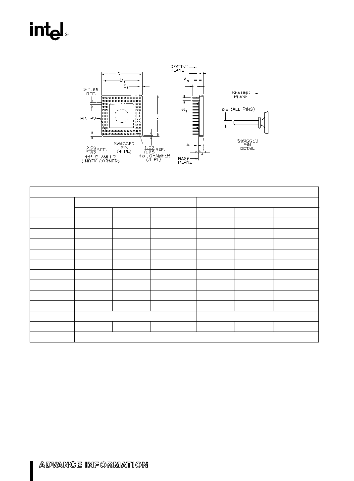
M80C186EB
88-LEAD CERAMIC PIN GRID ARRAY PACKAGE
271214 � 33
Family Ceramic Pin Grid Array Package
Symbol
Millimeters
Inches
Min
Max
Notes
Min
Max
Notes
A
3 56
4 57
0 140
0 180
A
1
0 76
1 27
Solid Lid
0 030
0 050
Solid Lid
A
2
2 67
3 43
Solid Lid
0 105
0 135
Solid Lid
A
3
1 14
1 40
0 045
0 055
B
0 43
0 51
0 017
0 020
D
33 91
34 67
1 335
1 365
D
1
30 35
30 61
1 195
1 205
e
1
2 29
2 79
0 090
0 110
L
2 54
3 30
0 100
0 130
N
88
88
S
1
1 27
2 54
0 050
0 100
ISSUE
IWS
10 12 88
55

M80C186EB
ERRATA
The current stepping (B step) of the M80C186EB
has the following known functional anomaly
An internal problem with the interrupt controller
may prevent an acknowledge cycle from occur-
ring on the INTA1 line after an interrupt on INT1
This error only occurs when INT1 is configured in
cascaded mode and a higher priority interrupt ex-
ists
Problem
An interrupt acknowledge for INT1 is not generat-
ed on INTA1 in some conditions
Condition
Another interrupt of higher priority occurs after
the decision is made to service Interrupt 1 but
before the expected acknowledge cycle on
INTA1
Configuration
1 Master mode
2 INT1 is in cascade mode and is enabled
3 An interrupt of higher priority than INT1 is en-
abled (i e
DMA
timers
serial ports
INT
lines)
Workaround
There are only two possible situations that might
cause this problem These with their correspond-
ing workarounds are described in the table below
Condition
Workaround
1
Only INT1 is
Use INT0 in cascaded
configured in cascade
mode instead or
mode and is also a
make INT1 the highest
lower priority than
priority interrupt
another interrupt
2
INT1 and INT0 are
Change the priority of
both in cascade mode
INT1 to the highest
and INT1 is of lower
priority of all interrupts
priority than another
interrupt
REVISION HISTORY
The first revision of this data sheet (271214-001) in-
dicated only 8 MHz and 13 MHz availability The
M80C186EB will also be available in a 16 MHz ver-
sion The cover and various other locations in the
data sheet reflect the additional product speed offer-
ing
The following list reflects the changes made be-
tween the -001 version and this -002 version of the
M80C186EB data sheet
1 Operating Conditions section updated to reflect
16 MHz Input clock frequency limits
2 DC Specifications section Added notes regard-
ing untested values added changed input leak-
age current and input current symbols and val-
ues added 16 MHz I
CC
I
ID
and I
PD
values
3 AC Specifications section Added full 16 MHz AC
Characteristics added note about untested val-
ues and reduced minimum output delays (T
CHOV
and T
CLOV
) for all speeds
4 Modified Errata section to reflect B-step known
errata (INT1 acknowledge anomaly)
INTEL CORPORATION 2200 Mission College Blvd Santa Clara CA 95052 Tel (408) 765-8080
INTEL CORPORATION (U K ) Ltd Swindon United Kingdom Tel (0793) 696 000
INTEL JAPAN k k Ibaraki-ken Tel 029747-8511
Printed in U S A M379 1296 2K HP DM
Military and Special Products