 | –≠–ª–µ–∫—Ç—Ä–æ–Ω–Ω—ã–π –∫–æ–º–ø–æ–Ω–µ–Ω—Ç: STEL-2105 | –°–∫–∞—á–∞—Ç—å:  PDF PDF  ZIP ZIP |
Document Outline
- FEATURES
- BENEFITS
- BLOCK DIAGRAM
- PACKAGE OUTLINE - 68-pin PLCC
- PIN CONFIGURATION
- PACKAGE OUTLINE - 64-pin TQFP
- PIN CONFIGURATION
- INTRODUCTION
- FUNCTION BLOCKS Ö DESCRIPTION
- INPUT SIGNAL DESCRIPTIONS
- OUTPUT SIGNAL DESCRIPTIONS
- MODE CONTROL (WRITE) REGIST7ERS
- STATUS (READ) REGISTERS
- DECIMAL, HEX AND BINARY ADDRESS EQUIVALENTS
- REGISTER SUMMARY - WRITE REGISTERS
- REGISTER SUMMARY - READ REGISTERS
- ELECTRICAL CHARACTERISTICS
- MICROPROCESSOR INTERFACE TIMING
- INPUT AND OUTPUT TIMING

R
STEL-2105
Data Sheet
STEL-2105
Digital Downconverter &
Bit Synchronizer/QPSK
Demodulator
For Cable Applications

STEL-2105
2
PRODUCT INFORMATION
TABLE OF CONTENTS
FEATURES AND BENEFITS ..............................................................................................
3
BLOCK DIAGRAM................................................................................................................
3
PACKAGE OUTLINE -- PLCC Package .............................................................................
4
PIN CONFIGURATION -- PLCC Package ........................................................................
4
PACKAGE OUTLINE -- TQFP Package .............................................................................
5
PIN CONFIGURATION -- TQFP Package ........................................................................
5
INTRODUCTION ..................................................................................................................
6
FUNCTION BLOCKS – DESCRIPTION...........................................................................
7
Control and Microprocessor Interface Block........................................................
7
Local Oscillator NCO Block......................................................................................
7
Downconverter Block...............................................................................................
7
Integrate and Dump Filter Block............................................................................
7
Symbol Integrator Block...........................................................................................
7
Symbol Timing Discriminator and Loop Filter Block.......................................
7
Symbol Timing NCO Block.....................................................................................
8
Carrier Discriminator and Loop Filter Block.......................................................
8
INPUT SIGNAL DESCRIPTIONS ......................................................................................
9
OUTPUT SIGNAL DESCRIPTIONS .................................................................................. 11
MODE CONTROL (WRITE) REGISTERS......................................................................... 12
STATUS (READ) REGISTERS ............................................................................................ 18
DECIMAL, HEX AND BINARY ADDRESS EQUIVALENTS ...................................... 20
REGISTER SUMMARY: MODE CONTROL REGISTERS............................................ 21
REGISTER SUMMARY: STATUS REGISTERS............................................................. 22
ELECTRICAL CHARACTERISTICS:
ABSOLUTE MAXIMUM RATINGS...................................................................... 23
RECOMMENDED OPERATING CONDITIONS................................................. 23
D.C. CHARACTERISTICS....................................................................................... 23
MICROPROCESSOR INTERFACE TIMING........................................................ 24
INPUT/OUTPUT TIMING...................................................................................... 25

PRODUCT INFORMATION
3
STEL-2105
FEATURES
s Complete Digital CMOS QPSK
Demodulator in a Single Package
s Fully programmable to operate up
to 8 Mbps
s Includes Digital Downconverter
s Carrier Discriminator Operates in
both PLL and AFC Modes
s Includes Carrier Tracking Oscillator
with Second Order Loop Filter
s Includes Symbol Timing
Discriminator and Oscillator
s Fully Programmable via Versatile
Microprocessor Interface
s 68-Pin PLCC or 64-Pin TQFP
Package Options
BENEFITS
s Low Power, High Reliability and
Performance With Low
Manufacturing Costs
s Programmable to Operate over a
Wide Range of Data Rates Without
Hardware Changes
s Permits Direct Sampling at I.F.
s Combines Fast Acquisition with
Coherent Demodulation
s Minimizes Component Count and
Adjustments in Production
s Very Accurate Symbol Timing with
Minimum Clock Jitter
s No Hardware Changes Required
when Changing Parameters
s Small Footprint, Surface Mount
BLOCK DIAGRAM
LOCAL
OSCILLATOR
NCO
DOWN
CONVERTER
INTEGRATE
& DUMP
FILTERS
ON-TIME
ACCUMULATOR
SIN
COS
CARRIER &
SAMPLING
FREQUENCY
CONTROL
REGISTERS
AFC
RXIN
7-0
CLK
EARLY
ACCUMULATOR
LATE
ACCUMULATOR
SYMBOL TIMING
DISCRIMINATOR
& LOOP FILTER
PLL & AFC
CARRIER
DISCRIMINATORS
& LOOP FILTER
IOUT
QOUT
SYMBOL
TIMING
NCO
SAMCLK
AGC
SYMCLK
AGC
8
2
µPMODE
RD
DATA
7-0
ADDR
4-0
CONTROL
& µP
INTER-
FACE
RESET
WR
CSEL
5
8
DSTB
INT
STEL-2105
4
PRODUCT INFORMATION
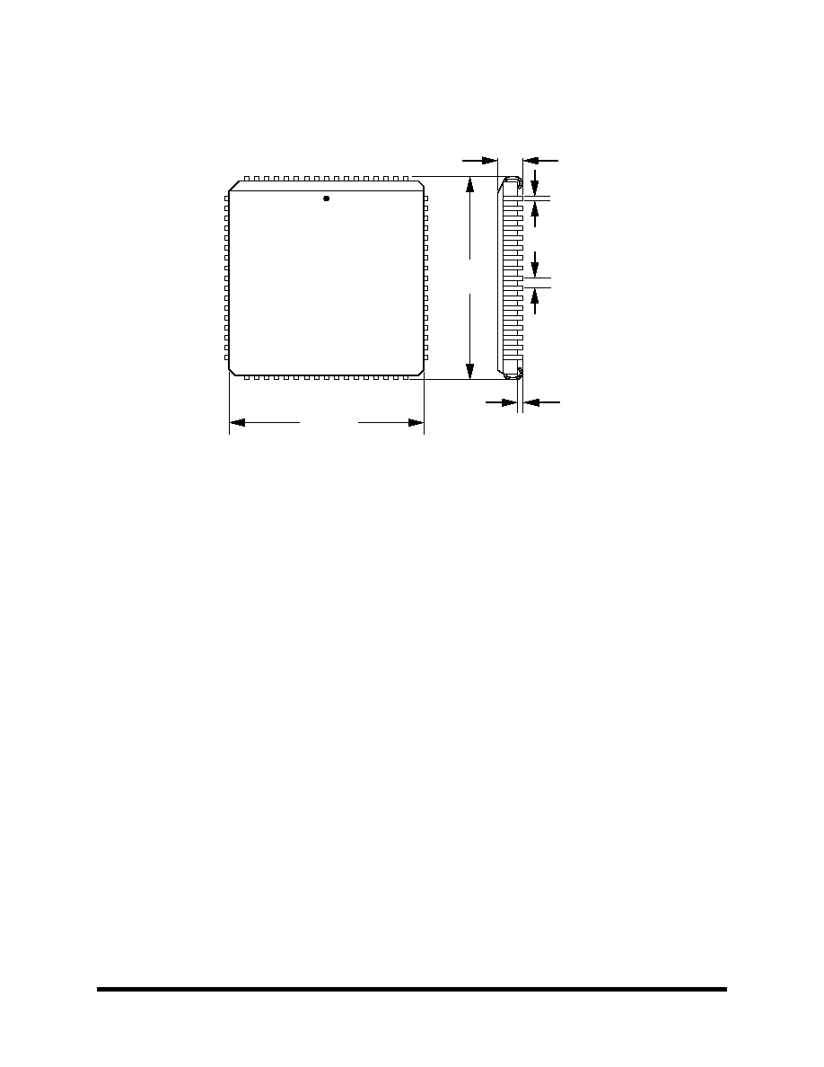
PACKAGE OUTLINE - 68-pin PLCC
60
59
58
57
56
55
54
53
52
51
50
49
48
47
46
45
44
2 2 2 3 3 3 3 3 3 3 3 3 3 4 4 4 4
7 8 9 0 1 2 3 4 5 6 7 8 9 0 1 2 3
6 6 6 6 6 6 6 6
9 8 7 6 5 4 3 2 1 8 7 6 5 4 3 2 1
10
11
12
13
14
15
16
17
18
19
20
21
22
23
24
25
26
0.200"
max.
0.990"
±0.005"
0.017"
± 0.004" (2)
At seating
plane
0.954"
± 0.004"
TOP
VIEW
0.05"
± 0.005" (1)
Tolerance not
cumulative
0.035"
nominal
Notes: (1) Tolerances on pin spacing are not cumulative
(2) Dimensions shown are at seating plane
(3) I.C. denotes Internal Connection. This pin must be left unconnected. Do not use for vias.
PIN CONFIGURATION
1
DATA
7
2
V
SS
3
V
SS
4
ADDR
4
5
ADDR
3
6
ADDR
2
7
ADDR
1
8
ADDR
0
9
V
DD
1 0
V
DD
1 1
CSEL
–––––
1 2
DSTB
–––––
1 3
WR
–––
1 4
RESET
––––––
1 5
RD
–––
1 6
µ
PMODE
1 7
CLK
1 8
V
SS
1 9
RXIN
7
2 0
RXIN
6
2 1
RXIN
5
2 2
RXIN
4
2 3
RXIN
3
2 4
RXIN
2
2 5
RXIN
1
2 6
RXIN
0
2 7
V
DD
2 8
I.C.
2 9
AGC
3 0
V
SS
3 1
I.C.
3 2
V
SS
3 3
N.C.
3 4
N.C.
3 5
V
SS
3 6
V
DD
3 7
I.C.
3 8
N.C.
3 9
SAMCLK
4 0
V
SS
4 1
I.C.
4 2
N.C.
4 3
V
DD
4 4
V
DD
4 5
I.C.
4 6
IOUT
4 7
I.C.
4 8
I.C.
4 9
QOUT
5 0
I.C.
5 1
I.C.
5 2
V
SS
5 3
SYMCLK
5 4
V
SS
5 5
V
SS
5 6
I.C.
5 7
V
SS
5 8
AFC
5 9
INT
–––
6 0
V
DD
6 1
V
DD
6 2
DATA
0
6 3
DATA
1
6 4
DATA
2
6 5
DATA
3
6 6
DATA
4
6 7
DATA
5
6 8
DATA
6
PRODUCT INFORMATION
5
STEL-2105
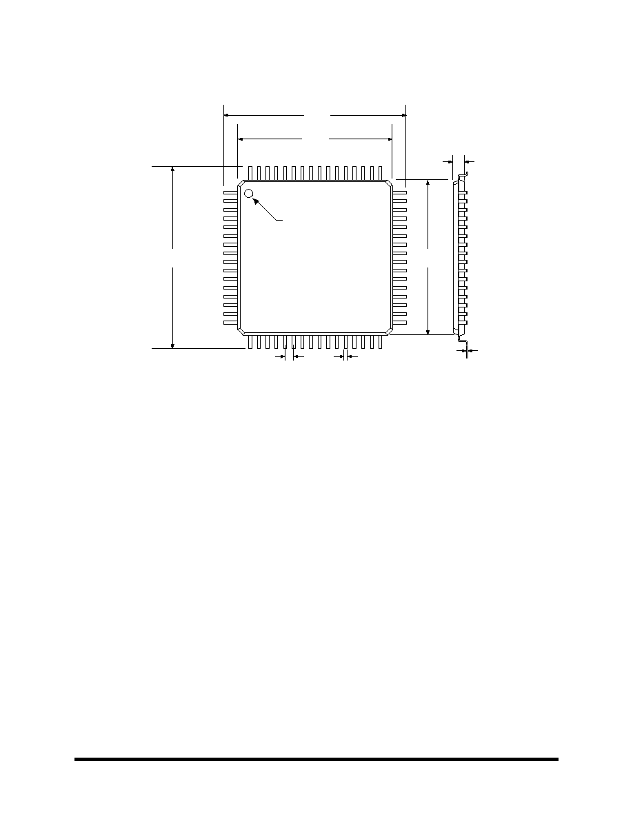
PACKAGE OUTLINE - 64-pin TQFP
TOP VIEW
PIN 1
INDICATOR
1
16
33
48
49
64
32
17
WBP 54598.c-9/10/98
0.055"
±
0.002"
0.004
±
0.002"
0.031"
±
0.005"
0.550"
±
0.002"
0.630"
±
0.005"
0.014"
±
0.002"
0.550"
±
0.002"
0.630"
±
0.005"
Notes: (1) Tolerances on pin spacing are not cumulative
(2) Dimensions shown are at seating plane
(3) I.C. denotes Internal Connection. This pin must be left unconnected. Do not use for vias.
(4) To order this package configuration, specify Model Number STEL-2105/CR
PIN CONFIGURATION
1
ADDR
0
2
V
DD
3
V
DD
4
CSEL
≠≠≠≠≠
5
DSTB
≠≠≠≠≠
6
WR
≠≠≠
7
RESET
≠≠≠≠≠≠
8
RD
≠≠≠
9
µ
PMODE
1 0
CLK
1 1
V
SS
1 2
RXIN
7
1 3
RXIN
6
1 4
RXIN
5
1 5
RXIN
4
1 6
RXIN
3
1 7
RXIN
2
1 8
RXIN
1
1 9
RXIN
0
2 0
V
DD
2 1
I.C.
2 2
AGC
2 3
V
SS
2 4
I.C.
2 5
V
SS
2 6
V
SS
2 7
V
DD
2 8
I.C.
2 9
SAMCLK
3 0
V
SS
3 1
I.C.
3 2
V
DD
3 3
V
DD
3 4
I.C.
3 5
IOUT
3 6
I.C.
3 7
I.C.
3 8
QOUT
3 9
I.C.
4 0
I.C.
4 1
V
SS
4 2
SYMCLK
4 3
V
SS
4 4
V
SS
4 5
I.C.
4 6
V
SS
4 7
AFC
4 8
INT
≠≠≠
4 9
V
DD
5 0
V
DD
5 1
DATA
0
5 2
DATA
1
5 3
DATA
2
5 4
DATA
3
5 5
DATA
4
5 6
DATA
5
57
DATA
6
5 8
DATA
7
5 9
V
SS
6 0
V
SS
6 1
ADDR
4
6 2
ADDR
3
6 3
ADDR
2
6 4
ADDR
1

STEL-2105
6
PRODUCT INFORMATION
INTRODUCTION
The STEL-2105 is a single ASIC which performs all
the digital processing required to implement a coherent
BPSK or QPSK demodulator. The device implements
all of the commonly used functions performed by the
STEL-2130A Digital downconverter and the STEL-
2110A Bit Synchronizer and PSK Demodulator ASICs.
The STEL-2105 is designed specifically for CATV
applications and provides an extremely low-cost
solution for the demodulation of QPSK signals at the
set-top decoder box.
The STEL-2105 operates at up to 4 Mbps in BPSK
mode and 8 Mbps in QPSK mode. It includes two
Numerically Controlled Oscillators (NCOs), one as the
local oscillator for carrier tracking and one as the
symbol timing generator. The local oscillator NCO
generates a quadrature signal which is mixed with the
input signal in a complex multiplier to perform down-
conversion directly from I.F. to baseband. A single
ADC is used to digitize the input signal, as described
in the applications section. The I.F. frequency is not
limited by the capabilities of the STEL-2105 but by the
track-and-hold capabilities of the ADC selected. Sig-
nals at I.F. frequencies up to about 100 MHz can be
processed by currently available 8-bit ADCs, but the
implementation cost, as well as the performance, can be
improved by using I.F. frequencies in the 30 MHz re-
gion or lower. The output of the downconverter is
then filtered with Integrate and Dump filters. These
have a sin(x)/x characteristic which is a function of
the number of samples integrated in each dump cycle.
The primary purpose of these filters is to allow the de-
vice to operate over a wide range of data rates using a
constant sampling rate, thereby eliminating the need to
change the anti-aliasing filter for each sampling rate.
The output rate of the Integrate and Dump filters
should be set to four samples per symbol to permit cor-
rect operation of the symbol timing circuit.
Symbol timing and clock recovery is performed by inte-
grating the four signal samples over a symbol period
using early and late integration relative to the on-time
signal used for the data. By integrating the samples
one quarter of a symbol early and late a
discrimination function is obtained which goes to zero
when the timing is correct, and this signal is used to
drive the symbol timing NCO via a loop filter. The
loop filter parameters are completely programmable
and can be changed during operation, allowing the
parameters to be optimized for fast acquisition and
tracking as well as maximum stability.
The carrier discriminator will generate both frequency
tracking (AFC) and phase tracking (PLL) functions.
The loop filter is programmable to operate with both
types of loops. This allows the device to be set up for
frequency tracking for fast carrier acquisition and
then switched to phase tracking for coherent demodu-
lation. A lock indicator function is provided to allow
the switch over to be done at the optimum time. The I
and Q channel outputs of the on-time integrator are
provided as the I and Q output bits.
The STEL-2105 is completely programmable via the
microprocessor interface. This interface has been
made very flexible to optimize direct interconnect with
a wide range of 8-bit microprocessors and microcom-
puter devices.

PRODUCT INFORMATION
7
STEL-2105
FUNCTION BLOCKS ≠ DESCRIPTION
Control and Microprocessor Interface
Block
Most of the functions of the STEL-2105 are pro-
grammed via the Control and Microprocessor Interface
Block. The setup and parameter information is written
into the twenty five 8-bit on-chip registers via the
microprocessor interface, and the contents of the
twenty one 8-bit status registers are also read out in
this way. The microprocessor interface has been
designed for optimum interconnection to most of the 8-
bit microprocessors and microcontrollers available.
Local Oscillator NCO Block
The STEL-2105 incorporates a Numerically Con-
trolled Oscillator (NCO) to synthesize a local oscil-
lator signal for the downconverter. The NCO is
clocked with the master clock signal, CLK. The NCO
has 32-bit frequency resolution and generates 8-bit
quadrature outputs. The frequency is controlled by
the data stored in the 32-bit Carrier Frequency Con-
trol Register as 4 bytes at addresses 10
H
to 13
H
. The
output of the Carrier Tracking Loop Filter is added to
or subtracted from this data to form the actual freq-
uency control information.
The frequencies of the Symbol Timing NCO and the
Local Oscillator NCO are both updated once every
symbol period during normal operation. However,
until the nominal symbol period information has been
written into the Symbol Timing NCO after a reset no
automatic updates will occur since the symbol
frequency will be set to zero. It is therefore necessary
to manually load the Symbol Timing NCO frequency
after a reset by setting bit 0 high. This will load both
NCOs. Bit 0 will automatically reset itself when this
is done.
Downconverter Block
The STEL-2105 incorporates a Half Quadrature
(Double Sideband) Downconverter which allows the
received signal to be sampled and digitized directly at
IF and converted to baseband digitally. The down-
converter includes two multipliers in which the 8-bit
receiver input signal is multiplied by the sine and
cosine signals from the NCO. All operations in the
downconverter are controlled by the main clock sig-
nal, CLK. In conjunction with the built-in frequency
tracking loop, this permits the received signal to be
downconverted accurately to baseband. The input
signal can be accepted in either Two’s Complement or
Offset Binary formats according to the setting of bit 2
in address 14
H
.
The outputs of the multipliers are:
I
OUT
= RXIN . cos(wt)
Q
OUT
= RXIN . sin(wt)
where w = 2
f
NCO
These are fed into the I and Q channel Integrate and
Dump Filters.
Integrate and Dump Filter Block
These filters integrate the downconverted samples
over the number of sample periods determined by the
dump rate. The dump rate is controlled by the Symbol
Timing NCO such that either four or five samples at the
dump rate occur in each symbol period, as determined
by the setting of bit 0 in address 16
H
. These samples
are then fed into the Symbol Integrator Block. Since
the accumulation process increases the magnitudes of
the signal values a selectable viewport is provided at
the outputs of the Integrate and Dump Filters to allow
the optimum output bits to be selected for the 8-bit in-
puts of the Symbol Integrator Block. The viewport is
controlled by the data stored in bits 3-0 in address
00
H
.
Symbol Integrator Block
The I and Q symbol information is generated in the
Symbol Integrator Block by integrating the input sam-
ples over one symbol period, which corresponds to
four or five sample periods, as determined by the sett-
ing of bit 0 in address 16
H
. The symbol timing dis-
criminator function is derived by repeating the integra-
tion process one sample early and one sample late rela-
tive to the nominally on-time integration, and these
signals are fed into the Symbol Timing Discriminator
and Loop Filter Block. The outputs of the I and Q
channel on-time integrators are the output symbols,
and two selectable viewports are provided to select
the optimum 8-bit values fed into the Carrier
Discriminator and Loop Filter Block. The signs of
these outputs are the output data bits available at the
IOUT
and QOUT pins.
Symbol Timing Discriminator and Loop
Filter Block
The symbol timing discriminator function is generated
from the difference between the sums of the absolute I
and Q values of the early and late integrations from
the Symbol Integrator Block.
i.e., {Abs (I
late
)+ Abs(Q
late
)} – {Abs (I
early
)+ Abs(Q
early
)}
This is a linear function of the symbol timing error that

STEL-2105
8
PRODUCT INFORMATION
goes to zero when the on-time signal is optimally timed.
The computation of the symbol timing discriminator
results in a 12-bit signal, and a selectable viewport is
provided to allow the appropriate output bits to be se-
lected for the 8-bit input of the Symbol Timing Loop
Filter. The viewport is controlled by the data stored
in bits 2-0 in address 01
H
.
The Loop Filter transfer function can be set up to be ei-
ther first or second order and the coefficient values
can be adjusted in powers of 2 from 2
0
to 2
21
.
The
overall transfer function is:
z
– 1
Transfer Fn. = K1 +
1
/
4
K2 . –––––––
1 – z
–1
The
1
/
4
factor is introduced because the signal in the
integrator path of the loop is divided by four after the
integrator by truncating the 2 LSBs of the signal. This
signal is then added to the signal in the direct path
such that the LSBs of the signals are aligned. The coef-
ficients K1 and K2 are determined by the data stored
in bits 4-0 in addresses 0B
H
and 0A
H
, respectively.
K1 and K2 can also be set to zero individually by sett-
ing bits 2 or 3, respectively, high in address 05
H
, giving
the user full control of the loop filter characteristics.
In addition, the value of the accumulator output in the
K2 path of the loop filter can be forced to limit at a
boundary (which applies to both positive and negative
accumulated values) set by the data stored in bits 3-0
in addresses 06
H
. The boundary function can be en-
abled or disabled, according to the setting of bit 0 in
address 15
H
.
Symbol Timing NCO Block
The STEL-2105 incorporates a Numerically Con-
trolled Oscillator (NCO) to synthesize a sampling
clock which is used as the dump function of the Inte-
grate and Dump Filters in the Downconverter block.
This clock is further divided by four or five, according
to the setting of bit 0 in address 16
H
, to provide the
symbol clock output, SYMCLK, so that the sampling
rate of the signal is synchronized to the symbol rate
for all further processing. The NCO is clocked with
the master clock signal, CLK. The NCO has 32-bit
frequency resolution and the effective length of the
accumulator is extended to 39 bits by means of an add-
itional 7-bit divider. This extends the lower end of the
frequency range of the sampling clock by an additional
seven octaves, thereby allowing the STEL-2105 to
operate at very low data rates while maintaining high
resolution in the sampling rate control. The sampling
clock is derived from one of the eight most significant
phase bits of the NCO, according to the data stored in
bits 3-1 of addresses 16
H
. Normally the MSB of the
accumulator itself (Bit 31) is used as the clock. Select-
ing successively higher order bits results in the clock
frequency being reduced by a factor of two each time,
and the frequency control word should be increased
accordingly to compensate for this. The frequency of
the NCO is controlled by the data stored in the 32-bit
Sampling Frequency Control Register as 4 bytes at
addresses 0C
H
to 0F
H
. The output of the Symbol Tim-
ing Loop Filter is added to or subtracted from this data
to form the actual sampling rate control information.
The frequencies of the Symbol Timing NCO and the
Local Oscillator NCO are both updated once every
symbol period during normal operation. However,
until the nominal symbol period information has been
written into the Symbol Timing NCO after a reset no
automatic updates will occur since the symbol
frequency will be set to zero. It is therefore necessary
to manually load the Symbol Timing NCO frequency
after a reset by setting bit 0 high. This will load both
NCOs. Bit 0 will automatically reset itself when this
is done.
Carrier Discriminator and Loop Filter
Block
The carrier frequency discriminator functions are de-
cision directed values derived from the I and Q signals.
These are used to generate AFC (frequency tracking)
and PLL (phase tracking) signals for the frequency ac-
quisition and tracking loop filter. The algorithm used
depends on the signal type, which is controlled by the
setting of bit 7 in address 14
H
, as well as the state of
the AFC input, which determines whether the AFC or
PLL tracking mode is used.
When the AFC input signal is set high the device will
operate in the AFC mode. In this mode the dot and
cross products of I and Q are generated. These are the
real and imaginary results of the complex multiplica-
tion of the current and previous symbols
If bit 7 is set low the discriminator circuit is set into
the QPSK/AFC mode, using the following algorithm to
compute the carrier discriminator function, CD:
CD
=
(Cross x Sign[Dot])
–
(Dot x
Sign[Cross])
The computation of the AFC discriminator results in
an 18-bit signal which is sign-extended to form a19-bit
value. A selectable viewport is provided to allow the
appropriate output bits to be selected for the 8-bit in-
put of the Loop Filter. This viewport is controlled by
the data stored in bits 3-0 in address 04
H
.

PRODUCT INFORMATION
9
STEL-2105
When the AFC input signal is set low the device will
operate in the PLL mode
If bit 7 is set low the discriminator circuit is set into
the QPSK/PLL mode. In this mode it is necessary to
set the carrier phase rotation to –45
∞
by setting bits 3
and 2 in address 15
H
to 11. The following algorithm is
then used to compute the carrier discriminator func-
tion, CD, using rotated versions, I
rot
and Q
rot
, of I and
Q:
Polarity of
I
Q
CD
+
+
–I
rot
–
+
Q
rot
–
–
I
rot
+
–
–Q
rot
The PLL discriminator output is an 8-bit value which,
therefore, does not require scaling before being fed into
the Loop Filter.
The Loop Filter transfer function can be set up to be
either first or second order and the coefficient values
can be adjusted in powers of 2 from 2
0
to 2
21
.
The
overall transfer function is:
z
– 1
Transfer Fn. = K1 +
1/
4
K2 . –––––––
1 – z
–1
The
1/
4
factor is introduced because the signal in the
integrator path of the loop is divided by four after the
integrator by truncating the 2 LSBs of the signal. This
signal is then added to the signal in the direct path
such that the LSBs of the signals are aligned. The co-
efficients K1 and K2 are determined by the data stored
in bits 4-0 in addresses 09
H
and 08
H
, respectively. K 1
and K2 can both be set to zero individually by setting
bits 0 or 1, respectively, high in address 05
H
, giving the
user full control of the loop filter characteristics.
––––––––––––––––––––––––––––––––––––––––––––––––––––
INPUT SIGNAL DESCRIPTIONS
RESET
≠≠≠≠≠≠≠
(Pin 14)
The RESET
––––––
input provides the master reset function
for the STEL-2100A. When is set low it will reset the
mode control registers, as well as the signals in all the
data paths, to zero. Normal operation of the circuit
will resume when RESET
––––––
returns to the high state.
CLK (Pin 17)
The CLK input is the master system clock. With the
exception of the generation of the AGC output, all in-
ternal operations occur, and all output signals change,
on the rising edges of CLK. This signal should nomin-
ally be a square wave with a maximum frequency is 3 6
MHz.
RXIN
7-0
(Pins 19 - 26)
The RXIN
7-0
input is an 8-bit port for signals from an
external A/D converter. The data may be in either
Two's Complement or Offset Binary format, according
to the setting of bit 2 in address 14
H
. The data on this
input is latched in on the rising edges of CLK.
AFC (Pin 58)
In the STEL-2100A,
carrier discrimination can be
achieved either by frequency or phase discrimination.
The frequency discriminator uses the dot and cross
products of the I and Q signals to generate the AFC
error for the frequency acquisition and tracking loop.
The phase discriminator computes the PLL error from
either the in-phase or the quadrature-phase data in
QPSK mode of operation. The PLL error can be
inverted by setting bit 4 of address 20 to a logic low
value. The algorithm used in both methods depends on
the signal type and is controlled by bit 7 of address 20.
When the AFC input is set high the frequency
discriminator is selected. When it is set low the phase
lock loop is selected.
DATA
7-0
(Pins 1, 68 - 62)
The
8-bit bi-directional DATA
7-0
bus is the micro-
processor interface bus that provides access to the int-
ernal registers. DATA
7-0
is used in conjunction with
the ADDR
4-0
, WR
–––
, DSTB
–––––
and R D
–––
signals to set the
values of the mode control registers and to read
internal status information. Please refer to the Mode
Configuration map (write mode register) and the Int-
ernal Status map (read mode register) for more details.
ADDR
4-0
(Pins 4 - 8)
ADDR
4-0
is a 5-bit address bus that selects the mode
control register location into which the information
provided on the DATA
7-0
bus will be written.
ADDR
4-0
is used in conjunction with WR
–––
and
DATA
7-0
to write the information into the registers.

STEL-2105
10
PRODUCT INFORMATION
CSEL
≠≠≠≠≠≠
(Pin 11)
The chip select function input, CSEL
–––––
, is provided to
enable or disable the microprocessor operation of the
STEL-2100A. When CSEL
–––––
is set high the ADDR
4-0
and WR
–––
become disabled and have no affect on the
device. When CSEL
–––––
is set low the device is in its
normal mode of operation and ADDR
4-0
and WR
–––
are
active.
µ
PMODE (Pin 16)
When
µ
PMODE
is set low, the device is configured to
interface with microprocessors that require an inter-
face using a Read/ Write
–––––
signal and a Data Strobe,
e.g., Z80, 68xx. In this mode, WR
–––
and DSTB
–––––
control
the read and write functions, with WR
–––
performing the
Read/ Write
–––––
function. When
µ
PMODE
is set high,
the device is configured to interface with
microprocessors that require an interface using
separate read and write signals, e.g., i 80XX. In this
mode the write operation is controlled by the WR
–––
signal and the read operation by the R D
–––
signal. In
this case, DSTB
–––––
is not used and should be tied low.
W R
≠≠≠≠
(Pin 13)
When
µ
PMODE
is set low, WR
–––
is used to enable
write or read functions of the microprocessor. In this
mode, DSTB
–––––
is used to latch information into the mode
control registers when WR
–––
is low. The mode control
registers are transparent latches while DSTB
–––––
is low
and the information will be latched when DSTB
–––––
returns high. When WR
–––
is high, internal status
information is available on the DATA
7-0
bus when
DSTB
–––––
is low. When
µ
PMODE
is set high, DSTB
–––––
should always be grounded, and WR
–––
is used to latch
information into the mode control registers. In this
mode, the read operation is controlled by the RD
–––
pin.
RD
≠≠≠
(Pin 15)
Read Bar.
When
µ
PMODE
is set low, R D
–––
is not
used and should be tied low. When
µ
PMODE
is set
high, RD
–––
is used to read data from the DATA
7-0
bus.
DSTB
≠≠≠≠≠≠
(Pin 12)
Data Strobe Bar.
When
µ
PMODE
is low, DSTB
–––––
is
used to write data into the write registers when WR
–––
is low and to read data from the read register when
WR
–––
is high. When
µ
PMODE
is set high, DSTB
–––––
should be tied low.

PRODUCT INFORMATION
11
STEL-2105
OUTPUT SIGNAL DESCRIPTIONS
IOUT, QOUT (Pins 46, 49)
These are the in-phase and quadrature-phase output
signals, respectively. They represent the signs of the
internal 11-bit outputs of the on-time accumulators..
SAMCLK (Pin 39)
The SAMCLK output is the internal sampling clock
signal which is used as the dump clock in the Integrate
and Dump Filter Block. SAMCLK is generated from
one of the MSBs of the phase output of the Symbol
Timing NCO, according to the data programmed into
bits 3-1 in address 16
H
. There will be four or five
cycles of SAMCLK for each cycle of SYMCLK, acc-
ording to the data programmed into bit 0 in address
16
H
.
SYMCLK (Pin 53)
The SYMCLK output is a clock occurring at the sym-
bol rate. This period is equal to four cycles of
the sample clock, SAMCLK, with a 50% duty cycle.
The falling edges of this signal can be used to strobe
the IOUT and QOUT data.
AGC (Pin 29)
This the AGC indicator output. AGC serves as a mea-
sure of the signal amplitude of the signal input,
RXIN
7-0
. This is done by comparing the top two MSBs
of RXIN. Using the internal Two’s Complement
format, whenever these bits are equal is an indication
that the magnitude of the current sample is less than
one half the peak value, as determined by the
saturation
limits of the Analog to Digital Converter.
Consequently, when the input signal level is high the
two MSBs will be different during some signal sample
periods, and by integrating the AGC pulses an AGC
control signal can be obtained. The polarity of the
AGC
function is programmable via bit 3 of address
14
H
. If this bit is set high then AGC will normally be
set low and will pulse high during sample periods
when the sample amplitudes are higher than one half of
the peak value. If this bit is set low then the AGC
output will be logically inverted. This signal is
asynchronous with respect to the CLK, its timing is
directly related to the edges of RXIN
7
and RXIN
6
.
INT
≠≠≠≠
(Pin 59)
The INT
–––
output will pulse low for two SYMCLK
cycles every 64 cycles of SYMCLK, indicating that the
value of SYMLOCK in the Symbol Lock Indicator
Register at address15
H
has been updated. This signal
can be used as an interrupt to the microprocessor to
read the new value of SYMLOCK.
STEL-2105
12
PRODUCT INFORMATION
MODE CONTROL (WRITE) REGIST7ERS
Address 00
H
:
Bits 0 through 3 -- Integrate and Dump
Filter Viewport Control
The magnitudes of the signals in the Integrate and
Dump Filters in the Downconverter section increases
as the number of accumulations is increased, so that
the word-length of the outputs signals can reach 1 7
bits. The STEL-2105 incorporates a data selector cir-
cuit to select any eight consecutive bits from the 17-bit
output of the I & D Filters for processing in the Symbol
Integrator Block. The significance of this 8 bit value is
determined by the data loaded into bits 3-0 in address
00
H
. The resulting 8 bit value provided to the
Matched Filter will be equivalent to the 17 bit value
divided by 2
n
, where n = the unsigned value of bits 3-0.
Bits 3-0 control the viewport of the Integrate and
Dump filter outputs as shown in Table 1:
Bits 3-0 I & D bits output to Symbol Int. Block
0
H
7-0
1
H
8-1
2
H
9-2
3
H
10-3
.....
....
.....
....
8
H
15-8
9
H
16-9
Table 1. Integrate & Dump Filter Viewport Control
If I and Q are larger than the range specified by the
scale factor, I and Q will be saturated to the maximum
or minimum values of the 8-bit number, i.e., 7F
H
or 80
H
.
Address 01
H
:
Bits 0 through 2 -- Symbol Timing
Discriminator Viewport Control
The Symbol Timing Discriminator produces a 12-bit
symbol timing error, E, as follows:
E = {Abs (I
late
)+ Abs(Q
late
)} – {Abs (I
early
)+ Abs(Q
early
)}
where I
late
and Q
late
are the accumulated late values of
I and Q over four or five samples, according to the set-
ting of bit 0 in address 16
H
, and I
early
and Q
early
are
the corresponding early values. This 12-bit value is
extended to 13 bits by sign extension. The STEL-2105
incorporates a data selector circuit to select any eight
consecutive bits from the 13-bit output of the Symbol
Timing Discriminator for processing in the Symbol Int-
egrator Loop Filter. The significance of this 8 bit
value is determined by the data loaded into bits 2-0 in
address 01
H
. The resulting 8 bit value provided to the
Matched Filter will be equivalent to the 13 bit value
divided by 2
n
, where n = the unsigned value of bits 2-0.
Bits 2-0 control the viewport of the Symbol Timing
Discriminator output as shown in Table 2:
Bits 3-0 Discriminator bits output to Loop Filter
0
H
7-0
1
H
8-1
2
H
9-2
3
H
10-3
4
H
11-4
5
H
12-5
Table 2. Symbol Timing Discriminator Viewport
Control
If the output is larger than the range specified by the
scale factor, it will be saturated to the maximum or
minimum values of the 8-bit number, i.e., 7F
H
or 80
H
.
Address 02
H
:
Bits 0 through 3 -- Symbol Lock
Accumulator Viewport Control
The symbol lock function, is computed by accumulating
the following function over a period of 64 symbols:
6 3
SYMLOCK =
{I+Q
on-time
–
9
/
16
{I+Q
late
+ I+Q
early
}
0
where I+Q
(time)
= I
(time)
+ Q
(time)
and (time) = on-time, late or early, as appropriate
SYMLOCK is calculated to an accuracy of 19 bits.
The STEL-2105 incorporates a data selector circuit to
select any eight consecutive bits from the 19-bit
SYMLOCK output and makes it available in the Sym-
bol Lock Indicator Register at address 15
H
. The sig-
nificance of this 8 bit value is determined by the data
PRODUCT INFORMATION
13
STEL-2105
loaded into bits 3-0 in address 02
H
. The resulting 8 bit
value written into the Symbol Lock Indicator Register
will be equivalent to the 19 bit value divided by 2
n
,
where n = the unsigned value of bits 3-0.
Bits 3-0 control the viewport of the Symbol Lock Acc-
umulator output as shown in Table 3:
Bits 3-0 SYMLOCK bits output to Register
0
H
7-0
1
H
8-1
2
H
9-2
3
H
10-3
.....
....
.....
....
8
H
15-8
9
H
16-9
A
H
17-10
B
H
18-11
Table 3. Symbol Lock Accumulator Viewport Control
If the output is larger than the range specified by the
scale factor, it will be saturated to the maximum or
minimum values of the 8-bit number, i.e., 7F
H
or 80
H
Address 03
H
:
Bits 0 and 1 -- On-Time Symbol
Integrator Viewport Control
The 11-bit outputs of the On-time I and Q Channel
Accumulators in the Symbol Integrator Block are used
as the inputs for the Carrier Discriminator function.
The STEL-2105 incorporates data selector circuits to
select any eight consecutive bits from the 11-bit out-
puts of the On-time Accumulators for processing in the
Carrier Discriminator. The significance of this 8 bit
value is determined by the data loaded into bits 1-0 in
address 03
H
. The resulting 8 bit value provided to the
Carrier Discriminator will be equivalent to the 11-bit
value divided by 2
n
, where n = the unsigned value of
bits 1-0.
Bits 1-0 control the viewport of the On-time Symbol
Integrator Block output as shown in Table 4:
Bits 1-0 On-Time Acc. bits output to Carr. Disc.
0
H
7-0
1
H
8-1
2
H
9-2
3
H
10-3
Table 4. On-Time Symbol Integrator Viewport Con-
trol
If the output is larger than the range specified by the
scale factor, it will be saturated to the maximum or
minimum values of the 8-bit number, i.e., 7F
H
or 80
H
.
Address 04
H
:
Bits 0 through 3 -- AFC Discriminator
Viewport Control
When the AFC input signal is set high the Carrier Dis-
criminator will operate in the AFC mode. In this mode
the dot and cross products of I and Q are generated.
These are the real and imaginary results of the complex
multiplication of the current and previous symbols.
If bit 7 is set low the discriminator circuit is set into
the QPSK/AFC mode, using the following algorithm to
compute the carrier discriminator function, CD:
CD
=
(Cross x Sign[Dot])
–
(Dot x
Sign[Cross])
The computation of the AFC discriminator results in
an 18-bit signal which is sign-extended to form a19-bit
value. The STEL-2105 incorporates a data selector
circuit to select any eight consecutive bits from the 19-
bit CD output for processing in the Carrier Tracking
Loop Filter. The significance of this 8 bit value is det-
ermined by the data loaded into bits 3-0 in address
04
H
. The resulting 8 bit value provided to the Loop
Filter will be equivalent to the 19 bit value divided by
2
n
, where n = the unsigned value of bits 3-0.
Bits 3-0 control the viewport of the AFC Discrimina-
tor output as shown in Table 5:
STEL-2105
14
PRODUCT INFORMATION
Bits 3-0 AFC bits output to Loop Filter
0
H
7-0
1
H
8-1
2
H
9-2
3
H
10-3
.....
....
.....
....
8
H
15-8
9
H
16-9
A
H
17-10
B
H
18-11
Table 5. AFC Discriminator Viewport Control
If the output is larger than the range specified by the
scale factor, it will be saturated to the maximum or
minimum values of the 8-bit number, i.e., 7F
H
or 80
H
Address 05
H
:
Bit 0 -- K1 Off in Carrier Tracking Loop
Filter
Setting this bit high will set the value of K1 in the
Carrier Tracking Loop Filter to zero, thereby dis-
abling the first order path in this loop filter.
Bit 1 -- K2 Off in Carrier Tracking Loop
Filter
Setting this bit high will set the value of K2 in the
Carrier Tracking Loop Filter to zero, thereby dis-
abling the second order path in this loop filter.
Bit 2 -- K1 Off in Symbol Timing
Tracking Loop Filter
Setting this bit high will set the value of K1 in the
Symbol Timing Tracking Loop Filter to zero, thereby
disabling the first order path in this loop filter (AFC
Mode).
Bit 3 -- K2 Off in Symbol Timing
Tracking Loop Filter
Setting this bit high will set the value of K2 in the
Symbol Timing Tracking Loop Filter to zero, thereby
disabling the second order path in this loop filter.
Address 06
H
:
Bits 0 through 3 -- Symbol Timing
Tracking Loop Filter Accumulator
Boundary
The output of the accumulator in the K2 path of the
Symbol Timing Tracking Loop Filter is provided with
a programmable boundary circuit which prevents the
magnitude of the output value from exceeding the set
boundary. This function is normally disabled and can
be enabled by setting bit 0 in address 15
H
high. Bits 0
to 4 in address 06
H
set the boundary value according
to the following equations:
Positive boundary value = 2
n+15
Negative boundary value = 2
31
+ 2
n+15
where n is the 5 bit Boundary Value
The magnitude values may range from 00 00 80 00
H
to
40 00 00 00
H
, as shown in Table 6:
Bits 3-0 Accumulator Output Value Range (– to +)
0
H
80 00 80 00
H
to 00 00 80 00
H
1
H
80 01 00 00
H
to 00 01 00 00
H
2
H
80 02 00 00
H
to 00 02 00 00
H
3
H
80 04 00 00
H
to 00 04 00 00
H
.....
....
.....
....
C
H
88 00 00 00
H
to 08 00 00 00
H
D
H
90 00 00 00
H
to 10 00 00 00
H
E
H
A0 00 00 00
H
to 20 00 00 00
H
F
H
C0 00 00 00
H
to 40 00 00 00
H
Table 6. Symbol Timing Tracking Loop Filter Accumu-
lator Bounded Values
Address 07
H
:
Bits 0 through 3 -- Carrier Tracking
Loop Filter Accumulator Boundary
The output of the accumulator in the K2 path of the
Carrier Tracking Loop Filter is provided with a prog-
rammable boundary circuit which prevents the magni-
tude of the output value from exceeding the set bound-
ary. This function is normally disabled and can be en-
abled by setting bit 1 in address 15
H
high. Bits 0 to 4
in address 07
H
set the boundary value according to the
following equations:
Positive boundary value = 2
n+15
Negative boundary value = 2
31
+ 2
n+15
where n is the 5 bit Boundary Value
The magnitude values may range from 00 00 80 00
H
to
40 00 00 00
H
, as shown in Table 7:

PRODUCT INFORMATION
15
STEL-2105
Bits 3-0 Accumulator Output Value Range (– to +)
0
H
80 00 80 00
H
to 00 00 80 00
H
1
H
80 01 00 00
H
to 00 01 00 00
H
2
H
80 02 00 00
H
to 00 02 00 00
H
3
H
80 04 00 00
H
to 00 04 00 00
H
.....
....
.....
....
C
H
88 00 00 00
H
to 08 00 00 00
H
D
H
90 00 00 00
H
to 10 00 00 00
H
E
H
A0 00 00 00
H
to 20 00 00 00
H
F
H
C0 00 00 00
H
to 40 00 00 00
H
Table 7. Carrier Tracking Loop Filter Accumulator
Bounded Values
Address 08
H
:
Bits 0 through 4 -- K2 Gain Value in
Carrier Tracking Loop Filter
Bits 0 to 4 control the gain factor K2 of the second or-
der Carrier Tracking Loop Filter path. The gain factor
multiplies the signal before the accumulator by the
value of 2
n
, where n is the 5 bit K2 Gain Value.
The value of n may range from 0 to 21 (15
H
), as shown
in Table 8:
Bits 4-0
Gain in K2 Path
00
H
2
0
01
H
2
1
.....
....
.....
....
14
H
2
2 0
15
H
2
2 1
Table 8. K2 Gain Values
Address 09
H
:
Bits 0 through 4 -- K1 Gain Value in
Carrier Tracking Loop Filter
Bits 0 to 4 control the gain factor K1 of the first order
Carrier Tracking Loop Filter path. The gain factor
multiplies the signal before the accumulator by the
value of 2
n
, where n is the 5 bit K1 Gain Value.
The value of n may range from 0 to 21 (15
H
), as shown
in Table 9:
Bits 4-0
Gain in K1 Path
00
H
2
0
01
H
2
1
.....
....
.....
....
14
H
2
2 0
15
H
2
2 1
Table 9. K1 Gain Values
Address 0A
H
:
Bits 0 through 4 -- K2 Gain Value in
Symbol Timing Tracking Loop Filter
Bits 4 to 0 control the gain factor K2 of the second or-
der Symbol Timing Tracking Loop Filter path. The
gain factor multiplies the signal before the accumulator
by the value of 2
n
, where n is the 5 bit K2 Gain Value.
The value of n may range from 0 to 21 (15
H
), as shown
in Table 10:
Bits 4-0
Gain in K2 Path
00
H
2
0
01
H
2
1
.....
....
.....
....
14
H
2
2 0
15
H
2
2 1
Table 10. K2 Gain Values
Address 0B
H
:
Bits 0 through 4 -- K1 Gain Value in
Symbol Timing Tracking Loop Filter
Bits 4 to 0 control the gain factor K1 of the first order
Symbol Timing Tracking Loop Filter path. The gain
factor multiplies the signal before the accumulator by
the value of 2
n
, where n is the 5 bit K1 Gain Value.
The value of n may range from 0 to 21 (15
H
), as shown
in Table 11:
STEL-2105
16
PRODUCT INFORMATION
Bits 4-0
Gain in K1 Path
00
H
2
0
01
H
2
1
.....
....
.....
....
14
H
2
2 0
15
H
2
2 1
Table 11. K1 Gain Values
Addresses 0C
H
through 0F
H
:
Symbol Timing NCO Frequency Control
W o r d
The internal Symbol Timing NCO is driven by a freq-
uency control word that is the sum of the timing dis-
criminator error value (generated in the demodulator)
and the 32-bit frequency control word stored in this
location (FCW). The four 8-bit registers at addresses
0C
H
through 0F
H
are used to store the 32-bit frequency
control word as shown in Table 12. The LSB of each
byte is stored in bit 0 of each register.
ADDR
0F
H
ADDR
0E
H
ADDR
0D
H
ADDR
0C
H
Bits 31-24
Bits 23-16
Bits 15-8
Bits 7-0
Table 12. Symbol Timing NCO FCW Storage
Addresses 10
H
through 13
H
:
Local Oscillator NCO Frequency
Control Word
The internal Local Oscillator NCO is driven by a
frequency control word that is the sum of the freq-
uency discriminator error value (generated in the dem-
odulator) and the 32-bit frequency control word
stored in this location (FCW). The four 8-bit registers
at addresses 10
H
through 13
H
are used to store the 32-
bit frequency control word as shown in Table 13. The
LSB of each byte is stored in bit 0 of each register.
ADDR
13
H
ADDR
12
H
ADDR
11
H
ADDR
10
H
Bits 31-24
Bits 23-16
Bits 15-8
Bits 7-0
Table 13. Local Oscillator NCO FCW Storage
Address 14
H
:
Bit 0 -- Unused
This bit should be set to 1 for normal operation.
Bit 1 -- Unused
This bit should be set to 0 for normal operation.
Bit 2 -- Two's Complement Input Select
The RXIN
7-0
input signal can be in either Two's Comp-
lement or Offset Binary formats. Since all internal
processing in the device operates on Two's Comple-
ment format signals it is necessary to convert the
RXIN
7-0
inputs when they are in the Offset Binary
format by inverting the MSBs.
When bit 2 in address 14
H
is set high the device ex-
pects Two's Complement format inputs on RXIN
7-0
.
When it is set low the device expects Offset Binary
format on RXIN
7-0
. In Two's Complement the 8 bit in-
put values range from –128 to +127 (80
H
to 7F
H
). In
Offset Binary, the values range from 0 to +255 (00
H
to
FF
H
).
Bit 3 -- Set-AGC-True
≠≠≠≠≠≠≠≠≠≠≠≠≠≠≠
This the AGC function is computed by comparing the
top two MSBs of RXIN
7-0
. The polarity of the AGC
function is programmable via bit 3. If bit 3 in address
14
H
is set low then AGC will normally be set low and
will pulse high during sample periods when the sample
amplitudes are higher than one half of the peak value.
If this bit is set high then the AGC output will be logi-
cally inverted.
Bit 4 -- Unused
This bit should be set to 0 for normal operation.
Bit 5 -- Unused
This bit should be set to 1 for normal operation.
Bit 6 -- Subtract Carrier Error
The carrier frequency error signal from the Carrier
Tracking Loop Filter can be added to or subtracted
from the data stored in the Carrier Frequency Control
Register to form the actual frequency control informa-
tion for the Local Oscillator NCO. Setting bit 6 in
address 14
H
high causes the frequency error signal to
be subtracted, and setting it low causes it to be added.
Bit 7 -- Unused
This bit should be set to 0 for normal operation.
Address 15
H
:
Bits 0 -- Symbol Timing Tracking Loop
Filter Accumulator Boundary Enable
The output of the accumulator in the K2 path of the
Symbol Timing Tracking Loop Filter is provided with
a programmable boundary circuit which prevents the
magnitude of the output value from exceeding the set
boundary. This function is normally disabled and can

PRODUCT INFORMATION
17
STEL-2105
be enabled by setting bit 0 in address 15
H
high.
Bits 1 -- Carrier Tracking Loop Filter
Accumulator Boundary Enable
The output of the accumulator in the K2 path of the
Carrier Tracking Loop Filter is provided with a prog-
rammable boundary circuit which prevents the magni-
tude of the output value from exceeding the set bound-
ary. This function is normally disabled and can be
enabled by setting bit 1 in address 15
H
high.
Bits 2 to 7 -- Unused
These bits should all be set to 1 for normal operation.
Address 16
H
:
Bit 0 -- Unused
This bit should be set to 1 for normal operation.
Bits 1 through 3 -- Sampling Clock
Scaling Control
The Symbol Timing NCO has 32-bit frequency resolu-
tion and the effective length of the accumulator is ex-
tended to 39 bits by means of an additional 7-bit
divider. This extends the lower end of the frequency
range of the sampling clock by an additional seven
octaves, thereby allowing the STEL-2105 to operate at
very low data rates while maintaining high resolution
in the sampling rate control. The sampling clock is der-
ived from one of the eight most significant phase bits of
the NCO, according to the data stored in bits 1-3.in
address 16
H
. The MSB of the accumulator itself (Bit
31) is normally used as the clock. Selecting succes-
sively higher order bits results in the clock frequency
being reduced by a factor of two each time, and the fre-
quency control word should be increased accordingly
to compensate for this, as shown in Table 14.
Bits 3-1
Acc. Bit Used
for Clock
FCW Compensation
Factor
0
H
3 1
2
0
1
H
3 2
2
1
2
H
3 3
2
2
3
H
3 4
2
3
4
H
3 5
2
4
5
H
3 6
2
5
6
H
3 7
2
6
7
H
3 8
2
7
Table 14. Sampling Clock Scaling Factors
Address 17
H
:
Bit 0 -- Load NCOs
The frequencies of the Symbol Timing NCO and the Lo-
cal Oscillator NCO are both updated once every sym-
bol period during normal operation. However, until
some non-zero information has been loaded into the
Symbol Timing NCO after a reset the symbol frequency
will be set to zero, and no automatic updates will
occur. It is therefore necessary to manually load the
Symbol Timing NCO frequency after a reset by setting
bit 0 in address 17
H
high. This will load both NCOs.
Bit 0 will automatically reset itself when this is done.
Address 18
H
:
Bit 0 -- Freeze Status Registers
With the exception of the Symbol Lock Indicator Regis-
ter (address 15
H
), the information stored in the Status
Registers changes at least once every symbol period. In
order to make it possible to read out the contents of
these registers more slowly the STEL-2105 is provided
with the Freeze Status Registers function. This is
implemented by setting bit 0 in address 18
H
high, after
which the register contents can be read any time during
(or after) the next symbol period. When this bit is set
high the current contents of the registers will he held
until it is set low again.
STEL-2105
18
PRODUCT INFORMATION
STATUS (READ) REGISTERS
Address 00
H
:
Local Oscillator Phase, Bits 2 through 9
The Local Oscillator NCO generates ten phase bits
which are used to address the sine and cosine look-up
table (LUT). The top eight bits (bits 9-2) are available
in address 00
H
. This information changes every cycle
of CLK.
Addresses 01
H
through 04
H
:
Carrier Tracking Loop Filter Output,
Bits 0 through 31
The output of the Carrier Tracking Loop Filter is
available in addresses 01
H
through 04
H
as shown in
Table 18:
ADDR
04
H
ADDR
03
H
ADDR
02
H
ADDR
01
H
Bits 31-24
Bits 23-16
Bits 15-8
Bits 7-0
Table 18. Carrier Tracking Loop Filter Output
Registers
Address 05
H
:
Scaled Carrier Tracking AFC
Discriminator Output, Bits 0 through 7
The 8-bit output of the Carrier Tracking AFC
Discriminator, after being scaled by the viewport, is
available in address 05
H
. This information changes
every symbol period.
Address 06
H
:
Carrier Tracking PLL Discriminator
Output, Bits 0 through 7
The 8-bit output of the Carrier Tracking PLL
Discriminator is available in address 06
H
. This
information changes every symbol period.
Address 07
H
:
Rotated Q-Channel Signal,
Bits 0 through 7
The 8-bit rotated Q channel signal is available in
address 07
H
. This information changes every symbol
period. The rotation is controlled by bits 2-3 in
address 15
H
.
Address 08
H
:
Rotated I-Channel Signal,
Bits 0 through 7
The 8-bit rotated I channel signal is available in
address 08
H
. This information changes every symbol
period. The rotation is controlled by bits 2-3 in
address 15
H
.
Addresses 09
H
and 0A
H
:
Cross Product Generator Output, Bits 0
through 15
The output of the Cross Product circuit is available in
addresses 09
H
and 0A
H
as shown in Table 19. This
information changes every symbol period:
ADDR
0A
H
ADDR
09
H
Cross Prod. Bits 15-8
Cross Prod. Bits 7-0
Table 19. Cross Product Output Registers
Addresses 0B
H
and 0C
H
:
Dot Product Generator Output, Bits 0
through 15
The output of the Dot Product circuit is available in
addresses 0B
H
and 0C
H
as shown in Table 20. This
information changes every symbol period:
ADDR
0C
H
ADDR
0B
H
Dot Prod. Bits 15-8
Dot Prod. Bits 7-0
Table 20. Cross Product Output Registers
Addresses 0D
H
through 10
H
:
Symbol Timing Tracking Loop Filter
Output, Bits 0 through 31
The output of the Symbol Timing Tracking Loop Filter
is available in addresses 0D
H
through 10
H
as shown
in Table 21. This information changes every symbol
period:
ADDR
10
H
ADDR
0F
H
ADDR
0E
H
ADDR
0D
H
Bits 31-24
Bits 23-16
Bits 15-8
Bits 7-0
Table 21. Carrier Tracking Loop Filter Output
Registers
Address 11
H
:
Symbol Timing Tracking Loop Filter
Input, Bits 0 through 7
The 8-bit input of the Symbol Timing Tracking Loop
Filter is available in address 11
H
. This information
changes every symbol period.
Address 12
H
:
Carrier Discriminator I-Channel Input,
Bits 0 through 7
The 8-bit I channel input of the Carrier Discriminator

PRODUCT INFORMATION
19
STEL-2105
is available in address 12
H
. This information changes
every symbol period.
Address 13
H
:
Carrier Discriminator Q-Channel Input,
Bits 0 through 7
The 8-bit Q channel input of the Carrier Discriminator
is available in address 13
H
. This information changes
every symbol period.
Address 14
H
:
Overflow Flag Register
Address 14 contains eight overflow flags, as described
below. They are all normally high, and active low.
Bit 0 -- Symbol Timing Discriminator
Viewport Overflow
The Viewport at the output of the Symbol Timing
Discriminator circuit is controlled by bits 0-2 in
address 01
H
. If the viewport setting is too low the
output may be saturated and bit 0 will be set low to
indicate this condition.
Bits 1 and 2 -- Not used
Bit 3 -- On-Time Symbol Integrator
Viewport Overflow in I Channel
The Viewport at the output of the On-Time Symbol
Integrator which scales signals for the Carrier
Discriminators is controlled by bits 0-1 in address
03
H
. If the viewport setting is too low the outputs may
be saturated and bit 3 will be set low to indicate that
this condition exists in the I Channel signal.
Bit 4 -- On-Time Symbol Integrator
Viewport Overflow in Q Channel
The Viewport at the output of the On-Time Symbol
Integrator which scales signals for the Carrier
Discriminators is controlled by bits 0-1 in address
03
H
. If the viewport setting is too low the outputs may
be saturated and bit 4 will be set low to indicate that
this condition exists in the Q Channel signal.
Bit 5 -- Symbol Timing Loop Filter
Accumulator Overflow
The output of the accumulator in the K2 path of the
Symbol Timing Tracking Loop Filter is provided with
a programmable boundary circuit which prevents the
magnitude of the output value from exceeding the set
boundary. This function is normally disabled and can
be enabled by setting bit 0 in address 15
H
high. The
boundary value is set according to the data stored in
bits 0 to 4 in address 06
H
. If the boundary function is
enabled and the value of the accumulator exceeds the
boundary then bit 5 will be set low to indicate this
condition. If the boundary function is disabled then
bit 5 will be set low if the accumulator itself
overflows.
Bit 6 -- Carrier Loop Filter Accumulator
Overflow
The output of the accumulator in the K2 path of the
Carrier Tracking Loop Filter is provided with a
programmable boundary circuit which prevents the
magnitude of the output value from exceeding the set
boundary. This function is normally disabled and can
be enabled by setting bit 0 in address 15
H
high. The
boundary value is set according to the data stored in
bits 0 to 4 in address 06
H
. If the boundary function is
enabled and the value of the accumulator exceeds the
boundary then bit 6 will be set low to indicate this
condition. If the boundary function is disabled then
bit 6 will be set low if the accumulator itself
overflows.
Bit 7 -- AFC Viewport Overflow
The Viewport at the output of the AFC Discriminator
circuit is controlled by bits 0-3 in address 04
H
. If the
viewport setting is too low the output may be
saturated and bit 7 will be set low to indicate this
condition.
Address 15
H
:
Symbol Lock Indicator, Bits 0 through 7
The symbol lock function, is computed by accumulating
the following function over a period of 64 symbols:
6 3
SYMLOCK =
{I+Q
on-time
–
9
/
16
{I+Q
late
+ I+Q
early
}
0
where I+Q
(time)
= I
(time)
+ Q
(time)
and (time) = on-time, late or early, as appropriate
SYMLOCK is calculated to an accuracy of 19 bits.
The STEL-2105 incorporates a data selector circuit to
select any eight consecutive bits from the 19-bit
SYMLOCK output and makes it available in the Sym-
bol Lock Indicator Register at address 15
H
. The sig-
nificance of this 8 bit value is determined by the data
loaded into bits 3-0 in address 02
H
. If the output is
larger than the range specified by the scale factor, it
will be saturated to the maximum or minimum values of
the 8-bit number, i.e., 7F
H
or 80
H
.

STEL-2105
20
PRODUCT INFORMATION
DECIMAL, HEX AND BINARY ADDRESS EQUIVALENTS
Dec.
Hex.
Binary
Dec.
Hex.
Binary
Dec.
Hex.
Binary
0
00
H
00000
1
01
H
00001
2
02
H
00010
3
03
H
00011
4
04
H
00100
5
05
H
00101
6
06
H
00110
7
07
H
00111
8
08
H
01000
9
09
H
01001
1 0
0A
H
01010
1 1
0B
H
01011
1 2
0C
H
01100
1 3
0D
H
01101
1 4
0E
H
01110
1 5
0F
H
01111
1 6
10
H
10000
1 7
11
H
10001
1 8
12
H
10010
1 9
13
H
10011
2 0
14
H
10100
2 1
15
H
10101
2 2
16
H
10110
2 3
17
H
10111
2 4
18
H
11000
PRODUCT INFORMATION
21
STEL-2105
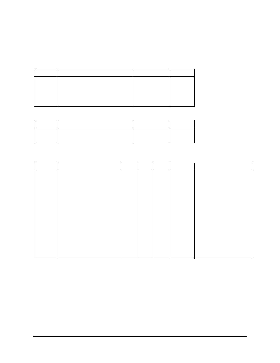
REGISTER SUMMARY - WRITE REGISTERS
Address
Contents
Bit 7
Bit 6
Bit 5
Bit 4
Bit 3
Bit 2
Bit 1
Bit 0
00
H
Integrate & Dump Filter Viewport Control
01
H
Symbol Error Scale Factor
02
H
Symbol Lock Scale Factor
03
H
Carr. Error Scale Factor
04
H
AFC Scale Factor
05
H
Sym. K2
off
Sym. K1
off
Car. K2 off Car. K1 off
06
H
Symbol K2 Boundary
07
H
Carrier K2 Boundary
08
H
Carrier Tracking Loop K2 Gain Value
09
H
Carrier Tracking Loop K1 Gain Value
0A
H
Symbol Timing K2 Gain Value
0B
H
Symbol Timing K1 Gain Value
0C-0F
H
Symbol Timing NCO Frequency Control Word (32 bits)
10-13
H
Local Oscillator NCO Frequency Control Word (32 bits)
14
H
Unused
(set to 0)
Inv.
Carrier
Loop Filter
Unused
(set to 1)
Unused
(set to 0)
AGC
Polarity
2’s Comp.
Input
Unused
(set to 0)
Unused
(set to 1)
15
H
Unused
(set all to 1)
En.
Carrier
Boundary
En. Symbol
Boundary
16
H
SAMCLK Select
Unused
(set to 1)
17
H
Load NCO
18
H
Freeze Regs

STEL-2105
22
PRODUCT INFORMATION
REGISTER SUMMARY - READ REGISTERS
Addres
s
Contents
Bit 7
Bit 6
Bit 5
Bit 4
Bit 3
Bit 2
Bit 1
Bit 0
00
H
Local Oscillator NCO Phase, Bits 9-2
01
H
Carrier Tracking Loop Filter Output, Bits 7-0
02
H
Carrier Tracking Loop Filter Output, Bits 15-8
03
H
Carrier Tracking Loop Filter Output, Bits 23-16
04
H
Carrier Tracking Loop Filter Output, Bits 31-24
05
H
Carrier AFC Discriminator Output, Bits 7-0
06
H
Carrier PLL Discriminator Output, Bits 7-0
07
H
Rotated Q Channel Signal
08
H
Rotated I Channel Signal
09
H
Cross Product Output, Bits 7-0
0A
H
Cross Product Output, Bits 15-8
0B
H
Dot Product Output, Bits 7-0
0C
H
Dot Product Output, Bits 15-8
0D
H
Symbol Tracking Loop Filter Output, Bits 7-0
0E
H
Symbol Tracking Loop Filter Output, Bits 15-8
0F
H
Symbol Tracking Loop Filter Output, Bits 23-16
10
H
Symbol Tracking Loop Filter Output, Bits 31-24
11
H
Symbol Tracking Loop Filter Input, Bits 7-0
12
H
Carrier Discriminator I Channel Input
13
H
Carrier Discriminator Q Channel Input
14
H
AFC
Viewport
Overflow
Carr. Trck.
Loop Filter
Acc. Ovfl.
Symb.Timing
Loop Filter
Acc. Ovfl.
Carr. Disc.
Q input
Overflow
Carr. Disc.
I input
Overflow
Not used
Symb.
Disc.
Viewport
Overflow
15
H
Symbol Lock Indicator
PRODUCT INFORMATION
23
STEL-2105
ELECTRICAL CHARACTERISTICS
ABSOLUTE MAXIMUM RATINGS
Warning
: Stresses greater than those shown below may cause permanent damage
to the device. Exposure of the device to these conditions for extended periods may
also affect device reliability. All voltages are referenced to V
SS
.
Symbol
Parameter
Range
Units
T
stg
Storage Temperature
–40 to +125
∞
C
V
DDmax
Supply voltage on V
DD
–0.3 to + 7
volts
V
I(max)
Input voltage
–0.3 to V
DD
+0.3
volts
I
i
DC input current
±
10
mA
RECOMMENDED OPERATING CONDITIONS
Symbol
Parameter
Range
Units
V
DD
Supply Voltage
+5
±
5%
volts
T
a
Operating Temperature (Ambient)
–40 to +85
∞
C
D.C. CHARACTERISTICS
Operating Conditions: V
DD
= 5.0 V
±
5%, V
SS
= 0 V, Ta = ≠40
∞
to 85
∞
C
Symbol
Parameter
Min.
Typ.
Max.
Units
Conditions
I
DDQ
Supply Current, Quiescent
1.0
mA
Static, no clock
I
DD
Supply Current, Operational
5
mA/MHz
f
CLK
= 36 MHz
V
IH(min)
High Level Input Voltage
2.0
volts
Logic '1'
V
IL(max)
Low Level Input Voltage
0.8
volts
Logic '0'
I
IH(min)
High Level Input Current
1 0
µ
A
CLK
only, V
IN
= V
DD
I
IH(min)
High Level Input Current
1 0
3 5
110
µ
A
All other inputs, V
IN
= V
DD
I
IL(max)
Low Level Input Current
–10
µ
A
All inputs, V
IN
= V
SS
V
OH(min)
High Level Output Voltage
2.4
4.5
V
DD
volts
I
O
= –2.0 mA,
All outputs
V
OL(max)
Low Level Output Voltage
0.2
0.4
volts
I
O
= +2.0 mA,
All outputs
I
OS
Output Short Circuit Current
2 0
6 5
130
mA
V
OUT
= V
DD
, V
DD
= max
C
IN
Input Capacitance
2
pF
All inputs
C
OUT
Output Capacitance
4
pF
All outputs
STEL-2105
24
PRODUCT INFORMATION
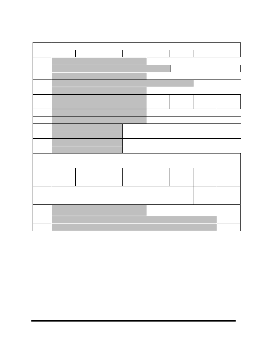
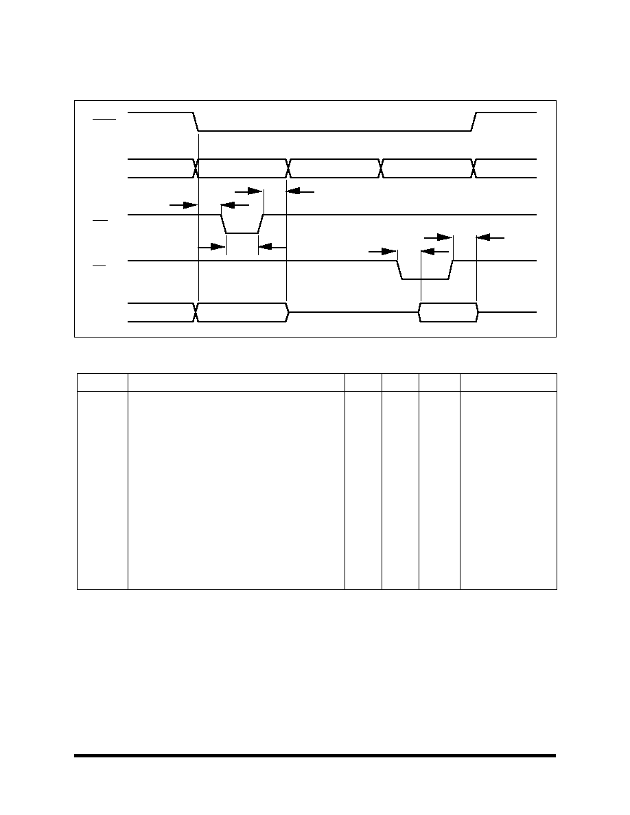
MICROPROCESSOR INTERFACE TIMING
t
W
ADDR
4-0
DON'T CARE
DON'T CARE
DATA
7-0
DON'T CARE
DON'T CARE
HI-Z
WRITE ADDR.
READ ADDR.
WRITE DATA
O/P DATA
t
SU1
t
HD1
t
ZV
t
VZ
CSEL
WR
RD
A.C. CHARACTERISTICS
Operating Conditions: V
DD
= 5.0 V
±
5%, V
SS
= 0 V, T
a
= ≠40
∞
to 85
∞
C,
Symbol
Parameter
Min.
Max.
Units
Conditions
t
SU1
CSEL
–––––
, ADDR, DATA to WR
–––
setup
5
nsec.
t
DH1
WR
–––
to CSEL
–––––
, ADDR, DATA hold
5
nsec.
t
W
WR
–––
pulse width
5
nsec.
t
ZV
DATA
Hi-Z to DATA valid
4 0
t
VZ
DATA
valid to DATA Hi-Z
4 0
t
SU2
RXIN
to CLK setup
3
nsec.
t
DH2
CLK
to RXIN hold
5
nsec.
t
IA
RXIN
stable to AGC valid
1 0
nsec.
t
CO
CLK
to output delays:
CLK
to SAMCLK delay
CLK
to SYMCLK delay
CLK
to IOUT/QOUT delay
2 8
1 3
2 8
nsec.
nsec.
nsec.
Load = 10 pF

25
STEL-2105
INPUT AND OUTPUT TIMING
CLK
RXIN
t
CH
t
CL
t
SU2
t
HD2
AGC
t
IA
t
CO
SAMCLK
IOUT, QOUT
t
CO
SYMCLK

Copyright © Intel Corporation, December 15, 1999.
All rights reserved
Information in this document is provided in connection with
IntelÆ products. No license, express or implied, by estoppel
or otherwise, to any intellectual property rights is granted by
this document. Except as provided in Intels Terms and Con-
ditions of Sale for such products, Intel assumes no liability
whatsoever, and Intel disclaims any express or implied
warranty, relating to sale and/or use of IntelÆ products in-
cluding liability or warranties relating to fitness for a particu-
lar purpose, merchantability, or infringement of any patent,
copyright or other intellectual property right. Intel products
are not intended for use in medical, life saving, or life sus-
taining applications.
Intel may make changes to specifications and product de-
scriptions at any time, without notice.
For Further Information Call or Write
INTEL CORPORATION
Cable Network Operation
350 E. Plumeria Drive, San Jose, CA 95134
Customer Service Telephone: (408) 545-9700
Technical Support Telephone: (408) 545-9799
FAX: (408) 545-9888