8-23
May 1999
CA3088E
AM Receiver Subsystem and
General-Purpose Amplifier Array
Features
∑ Excellent Overload Characteristics
∑ AGC for IF Amplifier
∑ Buffered Output Signal for Tuning Meter
∑ Internal Zener Diode Provides Voltage Regulation
∑ Two IF Amplifier Stages
∑ Low-Noise Converter and First IF Amplifier
∑ Low Harmonic Distortion (THD)
∑ Delayed AGC for RF Amplifier
∑ Terminals for Optional Inclusion of Tone Control
∑ Operates from Wide Range of Power Supplies:
V+ = 6V to 16V
∑ Optional AC and/or DC Feedback on Wide-Band
Amplifier
∑ Array of Amplifiers for General-Purpose Applications
∑ Suitable for Use With Optional External RF Stage,
Either MOS or Bipolar
∑ Related at:
- Refer to AN6022 for Application Note Information
Description
The CA3088E, a monolithic integrated circuit, is an AM sub-
system that provides the converter, IF amplifier, detector,
and audio preamplifier stages for an AM receiver.
The CA3088E also provides internal AGC for the first IF
amplifier stage, delayed AGC for an optional external RF
amplifier, a buffer stage to drive a tuning meter, and termi-
nals facilitating the optional use of a tone control.
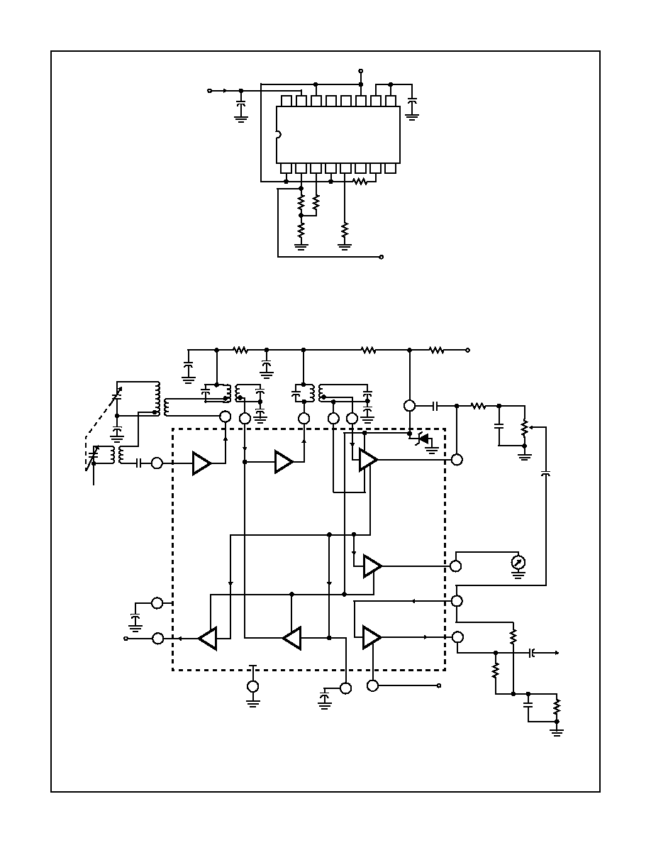
Figure 2 is a functional diagram of the CA3088E. The signal
from the low-noise converter is applied to the first IF ampli-
fier and is then coupled to the second IF amplifier. This IF
signal is then detected and externally filtered. The resultant
audio signal is applied to an audio preamplifier. Optionally, a
tone control circuit may be connected at the junction of the
detector circuit and the audio preamplifier. The gain of the
first IF amplifier stage is controlled by an internal AGC cir-
cuit. The CA3088E supplies a delayed AGC signal output for
use with an external RF amplifier. A buffered output signal is
also available for driving a tuning meter. A DC voltage, inter-
nally regulated by a Zener diode, supplies the second IF
amplifier, the AGC and tuning meter circuits and may also be
used with any other stage.
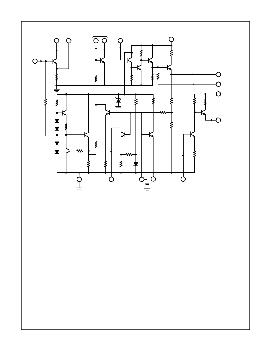
The CA3088E features four independent transistor amplifi-
ers, each incorporating internal biasing for temperature
tracking. These amplifiers are particularly useful in general-
purpose amplifier, oscillator, and detector applications in a
wide variety of equipment designs.
Pinout
CA3088E
(PDIP)
TOP VIEW
Part Number Information
PART NUMBER
TEMP.
RANGE (
o
C)
PACKAGE
PKG.
NO.
CA3088E
-40 to 85
16 Ld PDIP
E16.3
14
15
16
9
13
12
11
10
1
2
3
4
5
7
6
8
CONV. BYPASS
CONV. IN
CONV. OUT
1ST IF IN
GND
1ST IF OUT
2ND IF IN
2ND IF FB
AUDIO V+
AUDIO IN
RF AGC
TUNING METER
AGC FILTER
2ND IF V+
DET. OUT
AUDIO OUT
CAUTION: These devices are sensitive to electrostatic discharge. Users should follow proper IC Handling Procedures.
Copyright
©
Harris Corporation 1999
File Number
560.2
[ /Title
(CA30
88E)
/Sub-
ject
(AM
Receiv
er Sub-
sys-
tem
and
Gen-
eral-
Pur-
pose
Ampli-
fier
Array)
/Autho
r ()
/Key-
words
()
/Cre-
ator ()
/DOCI
NFO
pdf-
mark
[
/Page-
Mode
/Use-
Out-
lines
/DOC-
VIEW
pdf-
mark
OBSOLETE PR
ODUCT
NO RECOMMENDED REPLA
CEMENT
Call Central Applications 1-800-442-7747
or email: centapp@harris.com
8-24
Absolute Maximum Ratings
T
A
= 25
o
C
Thermal Information
Supply Voltage
(Across Term. 5 and Terms. 3, 6, 13, 16, Respectively) . . . . . 16V
Output Current
Terminals 3, 6, 13, 16, (Respectively). . . . . . . . . . . . . . . . . 10mA
Terminal 10 . . . . . . . . . . . . . . . . . . . . . . . . . . . . . . . . . . . . . 30mA
Operating Conditions
Temperature Range . . . . . . . . . . . . . . . . . . . . . . . . . -40
o
C to 85
o
C
Thermal Resistance (Typical, Note 1)
JA
(
o
C/W)
PDIP Package . . . . . . . . . . . . . . . . . . . . . . . . . . . . .
110
Maximum Junction Temperature (Plastic Package) . . . . . . . 150
o
C
Maximum Storage Temperature Range . . . . . . . . . -65
o
C to 150
o
C
Maximum Lead Temperature (Soldering 10s) . . . . . . . . . . . . 300
o
C
CAUTION: Stresses above those listed in "Absolute Maximum Ratings" may cause permanent damage to the device. This is a stress only rating and operation
of the device at these or any other conditions above those indicated in the operational sections of this specification is not implied.
NOTE:
1.
JA
is measured with the component mounted on an evaluation PC board in free air.
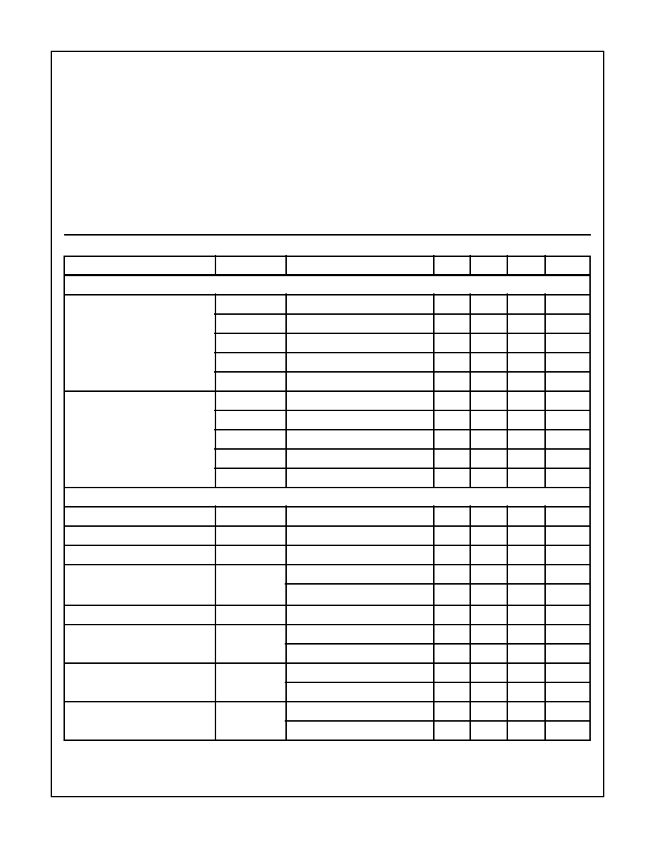
Electrical Specifications
T
A
= 25
o
C, V+ = 12V
PARAMETER
SYMBOL
TEST CONDITIONS
MIN
TYP
MAX
UNITS
DC CHARACTERISTICS
Voltage (Figure 1)
V
1
, V
4
, V
9
, V
11
Terminals 1, 4, 9, 11
-
0.7
-
V
V
2
, V
7
, V
8
Terminals 2, 7, 8
-
1.4
-
V
V
10
Terminal 10
-
5.6
-
V
V
12
Terminal 12
-
0
-
V
V
15
Terminal 15
-
3.5
-
V
Current (Figure 1)
I
3
Terminal 3
-
0.35
-
mA
I
6
Terminal 6
-
1.0
-
mA
I
10
Terminal 10
-
20
-
mA
I
13
Terminal 13
-
0
-
mA
I
16
Terminal 16
-
1.2
-
mA
DYNAMIC CHARACTERISTICS
Detector Output (Figure 2)
30% Modulation
-
75
-
mV
RMS
Audio Amplifier Gain (Figure 2)
A
AF
f = 1kHz
-
30
-
dB
Audio Distortion (Figure 2)
V
OUT
= 100mV
-
0.2
-
%
Sensitivity
(f
IN
= 1MHz, Signal-to-Noise Ratio
(S/N) = 20dB))
At Converter Stage Input (Figure 2)
-
200
-
µ
V/m
At RF Stage Input (Figure 2)
-
100
-
µ
V/m
Total Harmonic Distortion (Figure 2)
THD
30% Modulation
-
1.0
-
%
Input Resistance
(No AGC, f
IN
= 1MHz)
R
IN
At Transistor Q
1
-
3500
-
At Transistor Q
5
-
2000
-
Input Capacitance
(No AGC, f
IN
= 1MHz)
C
IN
At Transistor Q
1
-
17
-
pF
At Transistor Q
5
-
12
-
pF
Feedback Capacitance
(No AGC, f
IN
= 1MHz)
C
FB
At Transistor Q
1
-
1.5
-
pF
At Transistor Q
5
-
1.5
-
pF
CA3088E