 | –≠–ª–µ–∫—Ç—Ä–æ–Ω–Ω—ã–π –∫–æ–º–ø–æ–Ω–µ–Ω—Ç: CD4536BMS | –°–∫–∞—á–∞—Ç—å:  PDF PDF  ZIP ZIP |

7-1236
CAUTION: These devices are sensitive to electrostatic discharge; follow proper IC Handling Procedures.
1-888-INTERSIL or 321-724-7143 | Copyright © Intersil Corporation 1999
CD4536BMS
CMOS Programmable Timer
Description
CD4536BMS is a programmable timer consisting of 24 ripple
binary counter stages. The salient feature of this device is its
flexibility. The device can count from 1 to 2
24
or the first 8
stages can be bypassed to allow an output, selectable by a
4-bit code, from any one of the remaining 16 stages. It can
be driven by an external clock or an RC oscillator that can be
constructed using on-chip components. Input IN1 serves as
either the external clock input or the input to the on-chip RC
oscillator. OUT1 and OUT2 are connection terminals for the
external RC components. In addition, an on-chip monostable
circuit is provided to allow a variable pulse width output. Var-
ious timing functions can be achieved using combinations of
these capabilities.
A logic 1 on the 8-BYPASS input enables a bypass of the
first 8 stages and makes stage 9 the first counter stage of
the last 16 stages. Selection of 1 of 16 outputs is accom-
plished by the decoder and the BCD inputs A, B, C and D.
MONO IN is the timing input for the on-chip monostable
oscillator. Grounding of the MONO IN terminal through a
resistor of 10k
or higher, disables the one-shot circuit and
connects the decoder directly to the DECODE OUT terminal.
A resistor to VDD and a capacitor to ground from the MONO
IN terminal enables the one-shot circuit and controls its
pulse width.
A fast test mode is enabled by a logic 1 on 8-BYPASS, SET,
and RESET. This mode divides the 24-stage counter into
three 8-stage sections to facilitate a fast test sequence.
The CD4536BMS is supplied in these 16-lead outline packages:
Braze Seal DIP
H4X
Frit Seal DIP
H1F
Ceramic Flatpack
H6W
Features
∑ High Voltage Type (20V Rating)
∑ 24 Flip-Flop Stage - Counts from 2
0
to 2
24
∑ Last 16 Stages Selectable by BCD Select Code
∑ Bypass Input Allows Bypassing First 8 Stages
∑ On-Chip RC Oscillator Provision
∑ Clock Inhibit Input
∑ Schmitt Trigger in clock Line Permits Operation with
Very Long Rise and Fall Times
∑ On-Chip Monostable Output Provision
∑ Typical fCL = 3MHz at VDD = 10V
∑ Test Mode Allows Fast Test Sequence
∑ Set and Reset Inputs
∑ Capable of Driving Two Low Power TTL Loads, One
Lower Power Schottky Load, or Two HTL Loads Over
the Rated Temperature Range
∑ 100% Tested for Quiescent Current at 20V
∑ 5V, 10V and 15V Parametric Ratings
∑ Standardized, Symmetrical Output Characteristics
∑ Meets All Requirements of JEDEC Tentative Standard
No. 13B, "Standard Specifications for Description of
`B' Series CMOS Devices"
December 1992
File Number
3345
Pinout
CD4536BMS
TOP VIEW
14
15
16
9
13
12
11
10
1
2
3
4
5
7
6
8
SET
RESET
IN 1
OUT 1
OUT 2
8-BYPASS
VSS
CLOCK INHIBIT
VDD
OSC INHIBIT
DECODE OUT
D
C
B
A
MONO IN
BINARY
SELECT
Functional Diagram
OSC
14
6
9
10
11
12
1
2
15
A
B
C
D
BINARY
SELECT
8-BYPASS
INHIBIT
CLOCK
INHIBIT
SET
RESET
MONO IN
7
3
RS
4
5
OUT 1
OUT 2
RT
13 DECODE
OUT
IN 1
VSS = 8
VDD = 16
7-1237
Specifications CD4536BMS
Absolute Maximum Ratings
Reliability Information
DC Supply Voltage Range, (VDD) . . . . . . . . . . . . . . . -0.5V to +20V
(Voltage Referenced to VSS Terminals)
Input Voltage Range, All Inputs . . . . . . . . . . . . .-0.5V to VDD +0.5V
DC Input Current, Any One Input
. . . . . . . . . . . . . . . . . . . . . . . .±
10mA
Operating Temperature Range . . . . . . . . . . . . . . . . -55
o
C to +125
o
C
Package Types D, F, K, H
Storage Temperature Range (TSTG) . . . . . . . . . . . -65
o
C to +150
o
C
Lead Temperature (During Soldering) . . . . . . . . . . . . . . . . . +265
o
C
At Distance 1/16
±
1/32 Inch (1.59mm
±
0.79mm) from case for
10s Maximum
Thermal Resistance . . . . . . . . . . . . . . . .
ja
jc
Ceramic DIP and FRIT Package . . . . .
80
o
C/W
20
o
C/W
Flatpack Package . . . . . . . . . . . . . . . .
70
o
C/W
20
o
C/W
Maximum Package Power Dissipation (PD) at +125
o
C
For T
A
= -55
o
C to +100
o
C (Package Type D, F, K) . . . . . . 500mW
For T
A
= +100
o
C to +125
o
C (Package Type D, F, K). . . . . . Derate
Linearity at 12mW/
o
C to 200mW
Device Dissipation per Output Transistor . . . . . . . . . . . . . . . 100mW
For T
A
= Full Package Temperature Range (All Package Types)
Junction Temperature . . . . . . . . . . . . . . . . . . . . . . . . . . . . . . +175
o
C
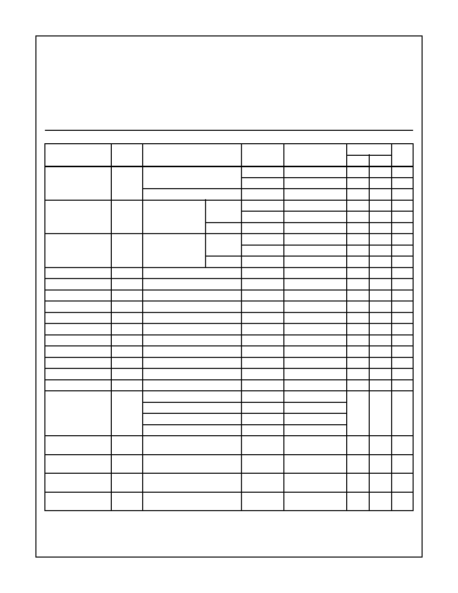
TABLE 1. DC ELECTRICAL PERFORMANCE CHARACTERISTICS
PARAMETER
SYMBOL
CONDITIONS (NOTE 1)
GROUP A
SUBGROUPS
TEMPERATURE
LIMITS
UNITS
MIN
MAX
Supply Current
IDD
VDD = 20V, VIN = VDD or GND
1
+25
o
C
-
10
µ
A
2
+125
o
C
-
1000
µ
A
VDD = 18V, VIN = VDD or GND
3
-55
o
C
-
10
µ
A
Input Leakage Current
IIL
VIN = VDD or GND
VDD = 20
1
+25
o
C
-100
-
nA
2
+125
o
C
-1000
-
nA
VDD = 18V
3
-55
o
C
-100
-
nA
Input Leakage Current
IIH
VIN = VDD or GND
VDD = 20
1
+25
o
C
-
100
nA
2
+125
o
C
-
1000
nA
VDD = 18V
3
-55
o
C
-
100
nA
Output Voltage
VOL15
VDD = 15V, No Load
1, 2, 3
+25
o
C, +125
o
C, -55
o
C
-
50
mV
Output Voltage
VOH15
VDD = 15V, No Load (Note 3)
1, 2, 3
+25
o
C, +125
o
C, -55
o
C 14.95
-
V
Output Current (Sink)
IOL5
VDD = 5V, VOUT = 0.4V
1
+25
o
C
0.53
-
mA
Output Current (Sink)
IOL10
VDD = 10V, VOUT = 0.5V
1
+25
o
C
1.4
-
mA
Output Current (Sink)
IOL15
VDD = 15V, VOUT = 1.5V
1
+25
o
C
3.5
-
mA
Output Current (Source)
IOH5A
VDD = 5V, VOUT = 4.6V
1
+25
o
C
-
-0.53
mA
Output Current (Source)
IOH5B
VDD = 5V, VOUT = 2.5V
1
+25
o
C
-
-1.8
mA
Output Current (Source)
IOH10
VDD = 10V, VOUT = 9.5V
1
+25
o
C
-
-1.4
mA
Output Current (Source)
IOH15
VDD = 15V, VOUT = 13.5V
1
+25
o
C
-
-3.5
mA
N Threshold Voltage
VNTH
VDD = 10V, ISS = -10
µ
A
1
+25
o
C
-2.8
-0.7
V
P Threshold Voltage
VPTH
VSS = 0V, IDD = 10
µ
A
1
+25
o
C
0.7
2.8
V
Functional
F
VDD = 2.8V, VIN = VDD or GND
7
+25
o
C
VOH >
VDD/2
VOL <
VDD/2
V
VDD = 20V, VIN = VDD or GND
7
+25
o
C
VDD = 18V, VIN = VDD or GND
8A
+125
o
C
VDD = 3V, VIN = VDD or GND
8B
-55
o
C
Input Voltage Low
(Note 2)
VIL
VDD = 5V, VOH > 4.5V, VOL < 0.5V
1, 2, 3
+25
o
C, +125
o
C, -55
o
C
-
1.5
V
Input Voltage High
(Note 2)
VIH
VDD = 5V, VOH > 4.5V, VOL < 0.5V
1, 2, 3
+25
o
C, +125
o
C, -55
o
C
3.5
-
V
Input Voltage Low
(Note 2)
VIL
VDD = 15V, VOH > 13.5V,
VOL < 1.5V
1, 2, 3
+25
o
C, +125
o
C, -55
o
C
-
4
V
Input Voltage High
(Note 2)
VIH
VDD = 15V, VOH > 13.5V,
VOL < 1.5V
1, 2, 3
+25
o
C, +125
o
C, -55
o
C
11
-
V
NOTES: 1. All voltages referenced to device GND, 100% testing being
implemented.
2. Go/No Go test with limits applied to inputs.
3. For accuracy, voltage is measured differentially to VDD. Limit
is 0.050V max.
7-1238
Specifications CD4536BMS
TABLE 2. AC ELECTRICAL PERFORMANCE CHARACTERISTICS
PARAMETER
SYMBOL
CONDITIONS (NOTE 1, 2)
GROUP A
SUBGROUPS
TEMPERATURE
LIMITS
UNITS
MIN
MAX
Propagation Delay
Clock to Q1 8-Bypass
High
TPHL1
TPLH1
VDD = 5V, VIN = VDD or GND
9
+25
o
C
-
2000
ns
10, 11
+125
o
C, -55
o
C
-
2700
ns
Propagation Delay
Clock to Q1 8-Bypass
Low
TPHL2
TPLH2
VDD = 5V, VIN = VDD or GND
9
+25
o
C
-
5000
ns
10, 11
+125
o
C, -55
o
C
-
6750
ns
Propagation Delay
Clock to Q16
TPHL3
TPLH3
VDD = 5V, VIN = VDD or GND
9
+25
o
C
-
8000
ns
10, 11
+125
o
C, -55
o
C
-
10800
ns
Propagation Delay
Reset to QN
TPHL4
VDD = 5V, VIN = VDD or GND
9
+25
o
C
-
6000
ns
10, 11
+125
o
C, -55
o
C
-
8100
ns
Transition Time
TTHL
TTLH
VDD = 5V, VIN = VDD or GND
9
+25
o
C
-
200
ns
10, 11
+125
o
C, -55
o
C
-
270
ns
Maximum Clock Input
Frequency
FCL
VDD = 5V, VIN = VDD or GND
9
+25
o
C
.5
-
MHz
10, 11
+125
o
C, -55
o
C
.37
-
MHz
NOTES:
1. VDD = 5V, CL = 50pF, RL = 200K, Input TR, TF < 20ns.
2. -55
o
C and +125
o
C limits guaranteed, 100% testing being implemented.
TABLE 3. ELECTRICAL PERFORMANCE CHARACTERISTICS
PARAMETER
SYMBOL
CONDITIONS
NOTES
TEMPERATURE
LIMITS
UNITS
MIN
MAX
Supply Current
IDD
VDD = 5V, VIN = VDD or GND
1, 2
-55
o
C, +25
o
C
-
5
µ
A
+125
o
C
-
150
µ
A
VDD = 10V, VIN = VDD or GND
1, 2
-55
o
C, +25
o
C
-
10
µ
A
+125
o
C
-
300
µ
A
VDD = 15V, VIN = VDD or GND
1, 2
-55
o
C, +25
o
C
-
10
µ
A
+125
o
C
-
600
µ
A
Output Voltage
VOL
VDD = 5V, No Load
1, 2
+25
o
C, +125
o
C, -
55
o
C
-
50
mV
Output Voltage
VOL
VDD = 10V, No Load
1, 2
+25
o
C, +125
o
C, -
55
o
C
-
50
mV
Output Voltage
VOH
VDD = 5V, No Load
1, 2
+25
o
C, +125
o
C, -
55
o
C
4.95
-
V
Output Voltage
VOH
VDD = 10V, No Load
1, 2
+25
o
C, +125
o
C, -
55
o
C
9.95
-
V
Output Current (Sink)
IOL5
VDD = 5V, VOUT = 0.4V
1, 2
+125
o
C
0.36
-
mA
-55
o
C
0.64
-
mA
Output Current (Sink)
IOL10
VDD = 10V, VOUT = 0.5V
1, 2
+125
o
C
0.9
-
mA
-55
o
C
1.6
-
mA
Output Current (Sink)
IOL15
VDD = 15V, VOUT = 1.5V
1, 2
+125
o
C
2.4
-
mA
-55
o
C
4.2
-
mA
Output Current (Source)
IOH5A
VDD = 5V, VOUT = 4.6V
1, 2
+125
o
C
-
-0.36
mA
-55
o
C
-
-0.64
mA
Output Current (Source)
IOH5B
VDD = 5V, VOUT = 2.5V
1, 2
+125
o
C
-
-1.15
mA
-55
o
C
-
-2.0
mA
Output Current (Source)
IOH10
VDD = 10V, VOUT = 9.5V
1, 2
+125
o
C
-
-0.9
mA
-55
o
C
-
-1.6
mA
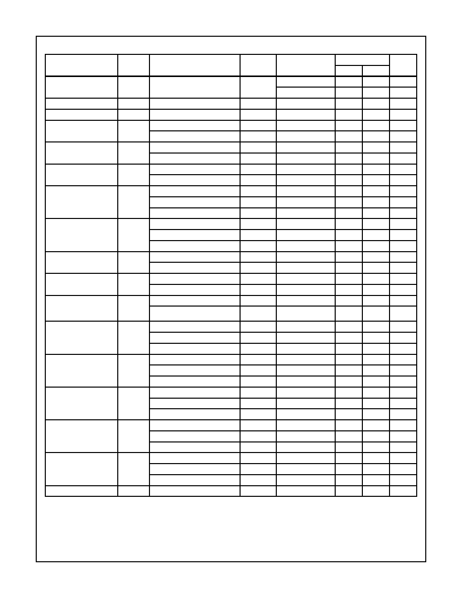
7-1239
Specifications CD4536BMS
Output Current (Source)
IOH15
VDD =15V, VOUT = 13.5V
1, 2
+125
o
C
-
-2.4
mA
-55
o
C
-
-4.2
mA
Input Voltage Low
VIL
VDD = 10V, VOH > 9V, VOL < 1V
1, 2
+25
o
C, +125
o
C, -55
o
C
-
3
V
Input Voltage High
VIH
VDD = 10V, VOH > 9V, VOL < 1V
1, 2
+25
o
C, +125
o
C, -55
o
C
+7
-
V
Propagation Delay
Clock to Q1 8-Bypass High
TPHL1
TPLH1
VDD = 10V
1, 2, 3
+25
o
C
-
1000
ns
VDD = 15V
1, 2, 3
+25
o
C
-
700
ns
Propagation Delay
Clock to Q1 8-Bypass Low
TPHL2
TPLH2
VDD = 10V
1, 2, 3
+25
o
C
-
1600
ns
VDD = 15V
1, 2, 3
+25
o
C
-
1200
ns
Propagation Delay
Clock to Q16
TPHL3
TPLH3
VDD = 10V
1, 2, 3
+25
o
C
-
3000
ns
VDD = 15V
1, 2, 3
+25
o
C
-
2000
ns
Propagation Delay
Qn to Qn+1
TPHL
TPLH
VDD = 5V
1, 2, 3
+25
o
C
-
300
VDD = 10V
1, 2, 3
+25
o
C
-
150
VDD = 15V
1, 2, 3
+25
o
C
-
100
Propagation Delay
Set to Qn
TPLH
VDD = 5V
1, 2, 3
+25
o
C
-
600
VDD = 10V
1, 2, 3
+25
o
C
-
250
VDD = 15V
1, 2, 3
+25
o
C
-
160
Propagation Delay
Reset to Qn
TPHL4
VDD = 10V
1, 2, 3
+25
o
C
-
2000
ns
VDD = 15V
1, 2, 3
+25
o
C
-
1500
ns
Transition Time
TTHL
TTLH
VDD = 10V
1, 2, 3
+25
o
C
-
100
ns
VDD = 15V
1, 2, 3
+25
o
C
-
80
ns
Maximum Clock Input
Frequency. Unlimited In-
put Rise or Fall Time
FCL
VDD = 10V
1, 2, 3
+25
o
C
1.5
-
MHz
VDD = 15V
1, 2, 3
+25
o
C
2.5
-
MHz
Minimum Clock Pulse
Width
TW
VDD = 5V
1, 2, 3
+25
o
C
-
400
ns
VDD = 10V
1, 2, 3
+25
o
C
-
150
ns
VDD = 15V
1, 2, 3
+25
o
C
-
100
ns
Minimum Set Pulse Width
TW
VDD = 5V
1, 2, 3
+25
o
C
-
400
ns
VDD = 10V
1, 2, 3
+25
o
C
-
200
ns
VDD = 15V
1, 2, 3
+25
o
C
-
120
ns
Minimum Reset Pulse
Width
TW
VDD = 5V
1, 2, 3
+25
o
C
-
6
µ
s
VDD = 10V
1, 2, 3
+25
o
C
-
2
µ
s
VDD = 15V
1, 2, 3
+25
o
C
-
1.5
µ
s
Minimum Set Recovery
Time
TREM
VDD = 5V
1, 2, 3
+25
o
C
-
5
µ
s
VDD = 10V
1, 2, 3
+25
o
C
-
2
µ
s
VDD = 15V
1, 2, 3
+25
o
C
-
1.6
µ
s
Minimum Reset Recov-
ery Time
TREM
VDD = 5V
1, 2, 3
+25
o
C
-
7
µ
s
VDD = 10V
1, 2, 3
+25
o
C
-
3
µ
s
VDD = 15V
1, 2, 3
+25
o
C
-
2
µ
s
Input Capacitance
CIN
Any Input
1, 2
+25
o
C
-
7.5
pF
NOTES:
1. All voltages referenced to device GND.
2. The parameters listed on Table 3 are controlled via design or process and are not directly tested. These parameters are characterized
on initial design release and upon design changes which would affect these characteristics.
3. CL = 50pF, RL = 200K, Input TR, TF < 20ns.
TABLE 3. ELECTRICAL PERFORMANCE CHARACTERISTICS
(Continued)
PARAMETER
SYMBOL
CONDITIONS
NOTES
TEMPERATURE
LIMITS
UNITS
MIN
MAX

7-1240
Specifications CD4536BMS
TABLE 4. POST IRRADIATION ELECTRICAL PERFORMANCE CHARACTERISTICS
PARAMETER
SYMBOL
CONDITIONS
NOTES
TEMPERATURE
LIMITS
UNITS
MIN
MAX
Supply Current
IDD
VDD = 20V, VIN = VDD or GND
1, 4
+25
o
C
-
25
µ
A
N Threshold Voltage
VNTH
VDD = 10V, ISS = -10
µ
A
1, 4
+25
o
C
-2.8
-0.2
V
N Threshold Voltage
Delta
VTN
VDD = 10V, ISS = -10
µ
A
1, 4
+25
o
C
-
±
1
V
P Threshold Voltage
VTP
VSS = 0V, IDD = 10
µ
A
1, 4
+25
o
C
0.2
2.8
V
P Threshold Voltage
Delta
VTP
VSS = 0V, IDD = 10
µ
A
1, 4
+25
o
C
-
±
1
V
Functional
F
VDD = 18V, VIN = VDD or GND
1
+25
o
C
VOH >
VDD/2
VOL <
VDD/2
V
VDD = 3V, VIN = VDD or GND
Propagation Delay Time
TPHL
TPLH
VDD = 5V
1, 2, 3, 4
+25
o
C
-
1.35 x
+25
o
C
Limit
ns
NOTES: 1. All voltages referenced to device GND.
2. CL = 50pF, RL = 200K, Input TR, TF < 20ns.
3. See Table 2 for +25
o
C limit.
4. Read and Record
TABLE 5. BURN-IN AND LIFE TEST DELTA PARAMETERS +25
o
C
PARAMETER
SYMBOL
DELTA LIMIT
Supply Current - MSI-2
IDD
±
1.0
µ
A
Output Current (Sink)
IOL5
±
20% x Pre-Test Reading
Output Current (Source)
IOH5A
±
20% x Pre-Test Reading
TABLE 6. APPLICABLE SUBGROUPS
CONFORMANCE GROUP
MIL-STD-883
METHOD
GROUP A SUBGROUPS
READ AND RECORD
Initial Test (Pre Burn-In)
100% 5004
1, 7, 9
IDD, IOL5, IOH5A
Interim Test 1 (Post Burn-In)
100% 5004
1, 7, 9
IDD, IOL5, IOH5A
Interim Test 2 (Post Burn-In)
100% 5004
1, 7, 9
IDD, IOL5, IOH5A
PDA (Note 1)
100% 5004
1, 7, 9, Deltas
Interim Test 3 (Post Burn-In)
100% 5004
1, 7, 9
IDD, IOL5, IOH5A
PDA (Note 1)
100% 5004
1, 7, 9, Deltas
Final Test
100% 5004
2, 3, 8A, 8B, 10, 11
Group A
Sample 5005
1, 2, 3, 7, 8A, 8B, 9, 10, 11
Group B
Subgroup B-5
Sample 5005
1, 2, 3, 7, 8A, 8B, 9, 10, 11, Deltas
Subgroups 1, 2, 3, 9, 10, 11
Subgroup B-6
Sample 5005
1, 7, 9
Group D
Sample 5005
1, 2, 3, 8A, 8B, 9
Subgroups 1, 2 3
NOTE: 1. 5% Parameteric, 3% Functional; Cumulative for Static 1 and 2.
TABLE 7. TOTAL DOSE IRRADIATION
CONFORMANCE GROUPS
MIL-STD-883
METHOD
TEST
READ AND RECORD
PRE-IRRAD
POST-IRRAD
PRE-IRRAD
POST-IRRAD
Group E Subgroup 2
5005
1, 7, 9
Table 4
1, 9
Table 4