 | –≠–ª–µ–∫—Ç—Ä–æ–Ω–Ω—ã–π –∫–æ–º–ø–æ–Ω–µ–Ω—Ç: EL400 | –°–∫–∞—á–∞—Ç—å:  PDF PDF  ZIP ZIP |

1
Æ
FN7156
CAUTION: These devices are sensitive to electrostatic discharge; follow proper IC Handling Procedures.
1-888-INTERSIL or 321-724-7143
|
Intersil (and design) is a registered trademark of Intersil Americas Inc.
Copyright © Intersil Americas Inc. 2003. All Rights Reserved. Elantec is a registered trademark of Elantec Semiconductor, Inc.
All other trademarks mentioned are the property of their respective owners.
EL400
200MHz Current Feedback Amplifier
The EL400 is a wide bandwidth, fast
settling monolithic amplifier built using
an advanced complementary bipolar
process. This amplifier uses current-mode feedback to
achieve more bandwidth at a given gain than conventional
operational amplifiers. Designed for closed-loop gains of ±1
to ±8, the EL400 has a 200MHz -3dB bandwidth (A
V
= +2),
and 12ns settling to 0.05% while consuming only 15mA of
supply current.
The EL400 is an obvious high-performance solution for video
distribution and line-driving applications. With low 15mA
supply current, differential gain/phase of 0.02%/0.01∞, and a
minimum 50mA output drive, performance in these areas is
assured.
The EL400's settling to 0.05% in 12ns, low distortion, and
ability to drive capacitive loads make it an ideal flash A/D
driver. The wide 200MHz bandwidth and extremely linear
phase allow unmatched signal fidelity. D/A systems can also
benefit from the EL400, especially if linearity and drive levels
are important.
Features
∑ 200MHz -3dB bandwidth, A
V
= 2
∑ 12ns settling to 0.05%
∑ V
S
= ±5V @ 15mA
∑ Low distortion: HD2, HD3 @
-60dBc at 20MHz
∑ Differential gain 0.02% at NTSC, PAL
∑ Differential phase 0.01∞ at NTSC, PAL
∑ Overload/short-circuit protected
∑ ±1 to ±8 closed-loop gain range
∑ Low cost
∑ Direct replacement for CLC400
Applications
∑ Video gain block
∑ Video distribution
∑ HDTV amplifier
∑ High-speed A/D conversion
∑ D/A I-V conversion
∑ Photodiode, CCD preamps
∑ IF processors
∑ High-speed communications
Pinout
EL400
(8-PIN PDIP, SO)
TOP VIEW
Ordering Information
PART
NUMBER
TEMP. RANGE
PACKAGE
PKG. NO.
EL400CN
-40∞C to +85∞C
8-Pin PDIP
MDP0031
EL400CS
-40∞C to +85∞C
8-Pin SO
MDP0027
Manufactured under U.S. Patent No. 4,893,091
Data Sheet
September 20, 2002
OBS
OLE
TE P
ROD
UCT
NO R
ECO
MME
NDE
D RE
PLA
CEM
ENT
cont
act o
ur Te
chni
cal S
uppo
rt Ce
nter
at
1-88
8-INT
ERS
IL or
www
.inte
rsil.c
om/t
sc
2
Absolute Maximum Ratings
(T
A
= 25∞C)
Supply Voltage (V
S
) . . . . . . . . . . . . . . . . . . . . . . . . . . . . . . . . . . .±7V
Output Current . . . . . . . . . . . . . . . . . . . . . . . . . . . . . . . . . . . . . . . . . .
Output is short-circuit protected to ground, however, maximum
reliability is obtained if I
OUT
does not exceed 70mA.
Common-Mode Input Voltage . . . . . . . . . . . . . . . . . . . . . . . . . . ±V
S
Differential Input Voltage . . . . . . . . . . . . . . . . . . . . . . . . . . . . . . . .5V
Power Dissipation . . . . . . . . . . . . . . . . . . . . . . . . . . . . . See Curves
Operating Temperature . . . . . . . . . . . . . . . . . . . . . . .-40∞C to +85∞C
Pin Temperature (Soldering, 5 Seconds). . . . . . . . . . . . . . . . . 300∞C
Junction Temperature . . . . . . . . . . . . . . . . . . . . . . . . . . . . . . . 175∞C
Storage Temperature . . . . . . . . . . . . . . . . . . . . . . . . -60∞C to +150∞C
Thermal Resistance:
. . . . . . . . . . . . . . . . . . . . . . . .
JA
= 95∞C/W PDIP
. . . . . . . . . . . . . . . . . . . . . . . . . . . . . . . . . . . . . . . .
JA
= 175∞C/W SO-8
CAUTION: Stresses above those listed in "Absolute Maximum Ratings" may cause permanent damage to the device. This is a stress only rating and operation of the
device at these or any other conditions above those indicated in the operational sections of this specification is not implied.
IMPORTANT NOTE: All parameters having Min/Max specifications are guaranteed. Typical values are for information purposes only. Unless otherwise noted, all tests
are at the specified temperature and are pulsed tests, therefore: T
J
= T
C
= T
A
Open-Loop DC Electrical Specifications
V
S
= ±5V, R
L
= 100
unless otherwise specified.
PARAMETER
DESCRIPTION
TEST CONDITIONS
TEMP
MIN
TYP
MAX
UNIT
V
OS
Input Offset Voltage
25∞C
2.0
5.5
mV
T
MIN
8.7
mV
T
MAX
9.5
mV
d(V
OS
)/d
T
Average Offset Voltage Drift
(Note 1)
All
10.0
40.0
µV/∞C
+I
IN
+Input Current
25∞C, T
MAX
10.0
25.0
µA
T
MIN
41.0
µA
d(+I
IN
)/d
T
Average +Input Current Drift
(Note 1)
All
50.0
200.0
nA/∞C
-I
IN
-Input Current
25∞C
10.0
25.0
µA
T
MIN
41.0
µA
T
MAX
35.0
µA
d(-I
IN
)/dT
Average -Input Current Drift
(Note 1)
All
100.0
200.0
nA/∞C
PSRR
Power Supply Rejection Ratio
All
40.0
50.0
dB
CMRR
Common-Mode Rejection Ratio
All
40.0
50.0
dB
I
S
Supply Current--Quiescent
No Load
All
15.0
23.0
mA
+R
IN
+Input Resistance
25∞C, T
MAX
100.0
200.0
k
T
MIN
50.0
k
C
IN
Input Capacitance
All
0.5
2.0
pF
R
OUT
Output Impedance (DC)
All
0.1
0.2
W
CMIR
Common-Mode Input Range
(Note 2)
25∞C, T
MAX
2.0
2.1
V
T
MIN
1.2
V
I
OUT
Output Current
25∞C, T
MAX
50.0
70.0
mA
T
MIN
35.0
mA
V
OUT
Output Voltage Swing
No Load
All
3.2
3.5
V
V
OUTL
Output Voltage Swing
100
25∞C
3.0
3.4
V
R
OL
Transimpedance
25∞C
30.0
125.0
V/mA
T
MIN
80.0
V/mA
T
MAX
140.0
V/mA
NOTES:
1. Measured from T
MIN
to T
MAX
.
2. Common-Mode Input Range for Rated Performance.
EL400

3
Closed-Loop AC Electrical Specifications
V
S
= ±5V, R
F
= 250
, A
V
= +2, R
L
= 100
unless otherwise specified.
PARAMETER
DESCRIPTION
TEST
CONDITIONS
TEMP
MIN
TYP
MAX
UNITS
Frequency
Response
SSBW
-3dB Bandwidth
(V
OUT
< 0.5V
PP
)
25∞C
150.0
200.0
MHz
T
MIN
150.0
MHz
T
MAX
120.0
MHz
LSBW
-3dB Bandwidth
(V
OUT
< 5.0V
PP
)
A
V
= +5
All
35.0
50.0
MHz
Gain Flatness
GFPL
Peaking
V
OUT
< 0.5V
PP
< 40MHz
25∞C
0.0
0.3
dB
T
MIN
, T
MAX
0.4
dB
GFPH
Peaking
V
OUT
< 0.5V
PP
> 40MHz
25∞C
0.0
0.5
dB
T
MIN
, T
MAX
0.7
dB
GFR
Rolloff
V
OUT
< 0.5V
PP
< 75MHz
25∞C
0.6
1.0
dB
T
MIN
1.0
dB
T
MAX
1.3
dB
LPD
Linear Phase Deviation
V
OUT
< 0.5V
PP
< 75MHz
25∞C, T
MIN
0.2
1.0
∞
T
MAX
1.2
∞
Time-Domain
Response
t
R1
, t
F1
Rise Time, Fall Time
0.5V Step
25∞C, T
MIN
1.6
2.4
ns
T
MAX
2.9
ns
t
R2
, t
F2
Rise Time, Fall Time
5.0V Step
All
6.5
10.0
ns
t
S1
Settling Time to 0.1%
2.0V Step
All
10.0
13.0
ns
t
S2
Settling Time to 0.05%
2.0V Step
All
12.0
15.0
ns
OS
Overshoot
0.5V Step
25∞C
0.0
10.0
%
T
MIN
, T
MAX
15.0
%
SR
Slew Rate
A
V
= +2
All
430.0
700.0
V/µs
A
V
= - 2
All
1600.0
V/µs
Distortion
HD2
2nd Harmonic Distortion at
20MHz
2V
PP
25∞C
-60.0
-45.0
dBc
T
MIN
-40.0
dBc
T
MAX
-45.0
dBc
HD3
3rd Harmonic Distortion at
20MHz
2V
PP
25∞C
-60.0
-50.0
dBc
T
MIN
, T
MAX
-50.0
dBc
Equivalent Input
Noise
NF
Noise Floor
> 100kHz
(Note 1)
25∞C
-157.0
-154.0
dBm (1Hz)
T
MIN
-154.0
dBm (1Hz)
T
MAX
-153.0
dBm (1Hz)
INV
Integrated Noise
100kHz to 200MHz
(Note 1)
25∞C
40.0
57.0
µV
T
MIN
57.0
µV
T
MAX
63.0
µV
Video Performance
d
G
Differential Gain (Note 2)
NTSC/PAL
25∞C
0.02
%
PP
d
P
Differential Phase (Note 2)
NTSC/PAL
25∞C
0.01
∞
PP
d
G
Differential Gain (Note 2)
30MHz
25∞C
0.05
%
PP
d
P
Differential Phase (Note 2)
30MHz
25∞C
0.05
∞
PP
VBW
-0.1dB Bandwidth (Note 2)
25∞C
60.0
MHz
NOTES:
1. Noise Tests are Performed from 5MHz to 200MHz.
2. Differential Gain/Phase Tests are R
L
= 100
. For other values of R
L
, see curves.
EL400
4
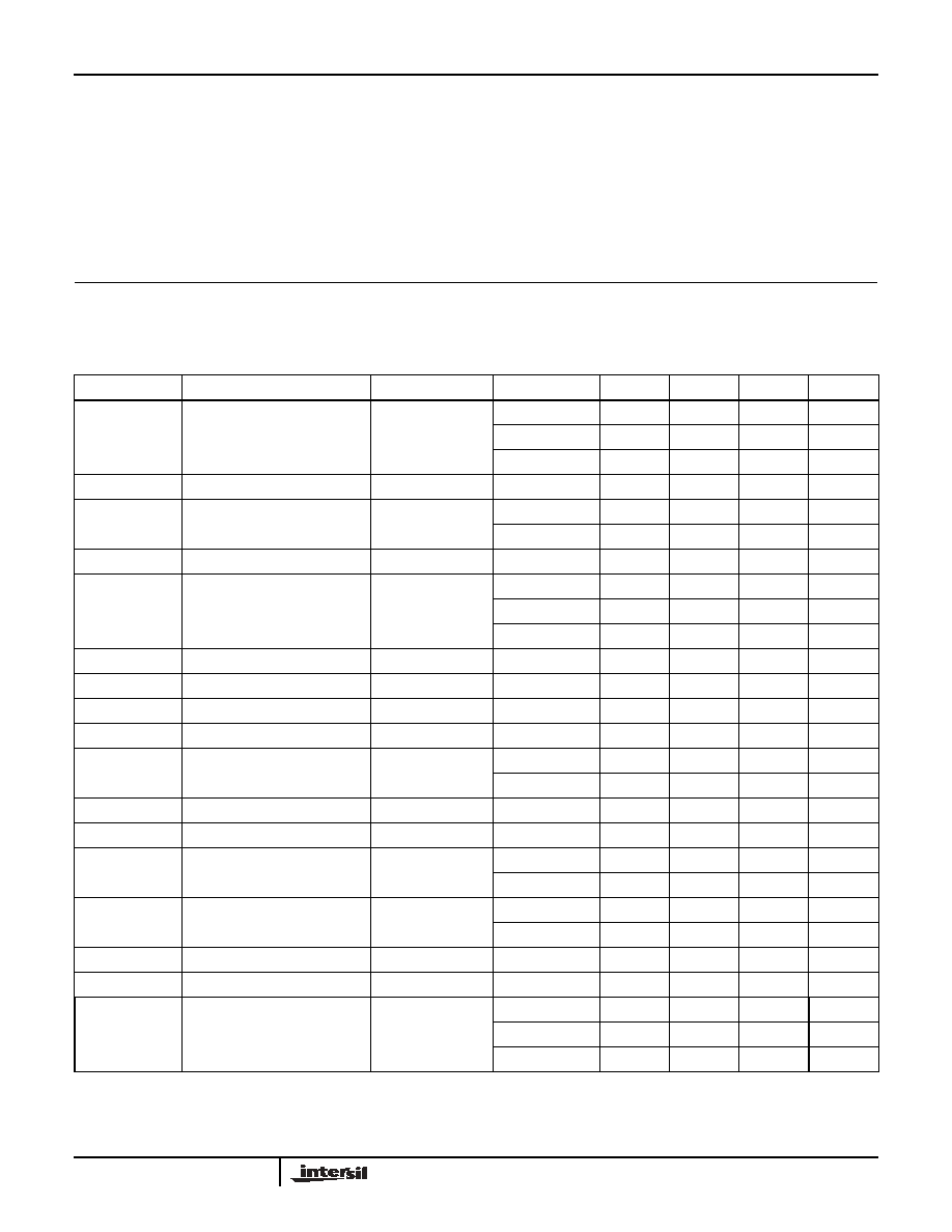
Typical Performance Curves
Non-Inverting
Frequency Response
Inverting Frequency
Response
Frequency Response for
Various R
L
s
Open-Loop Transimpedance
Gain and Phase
2nd and 3rd
Harmonic Distortion
2-Tone 3rd Order
Intermodulation Intercept
Equivalent Input Noise
Power-Supply
Rejection Ratio
Common-Mode
Rejection Ratio
Settling Time
Long-Term Settling Time
Settling Time vs
Load Capacitance
EL400
5
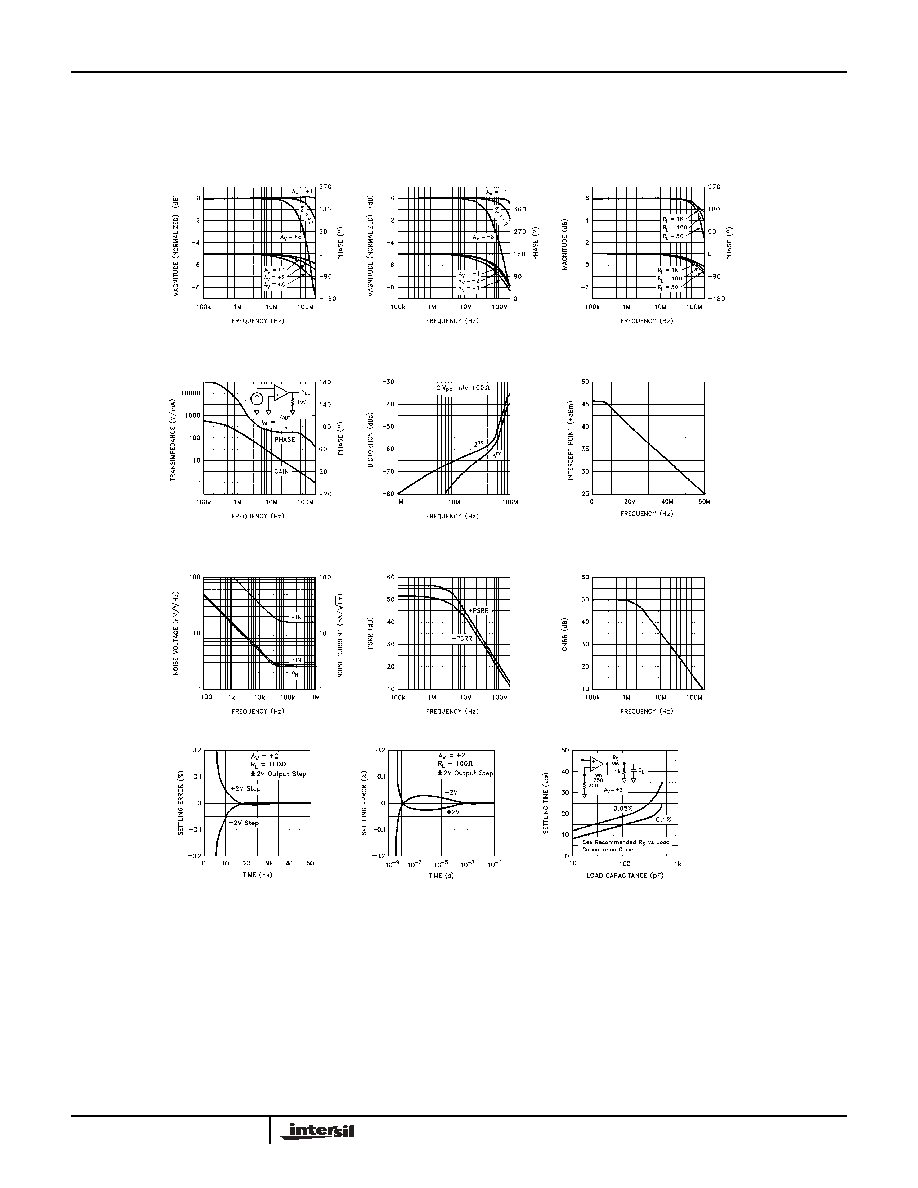
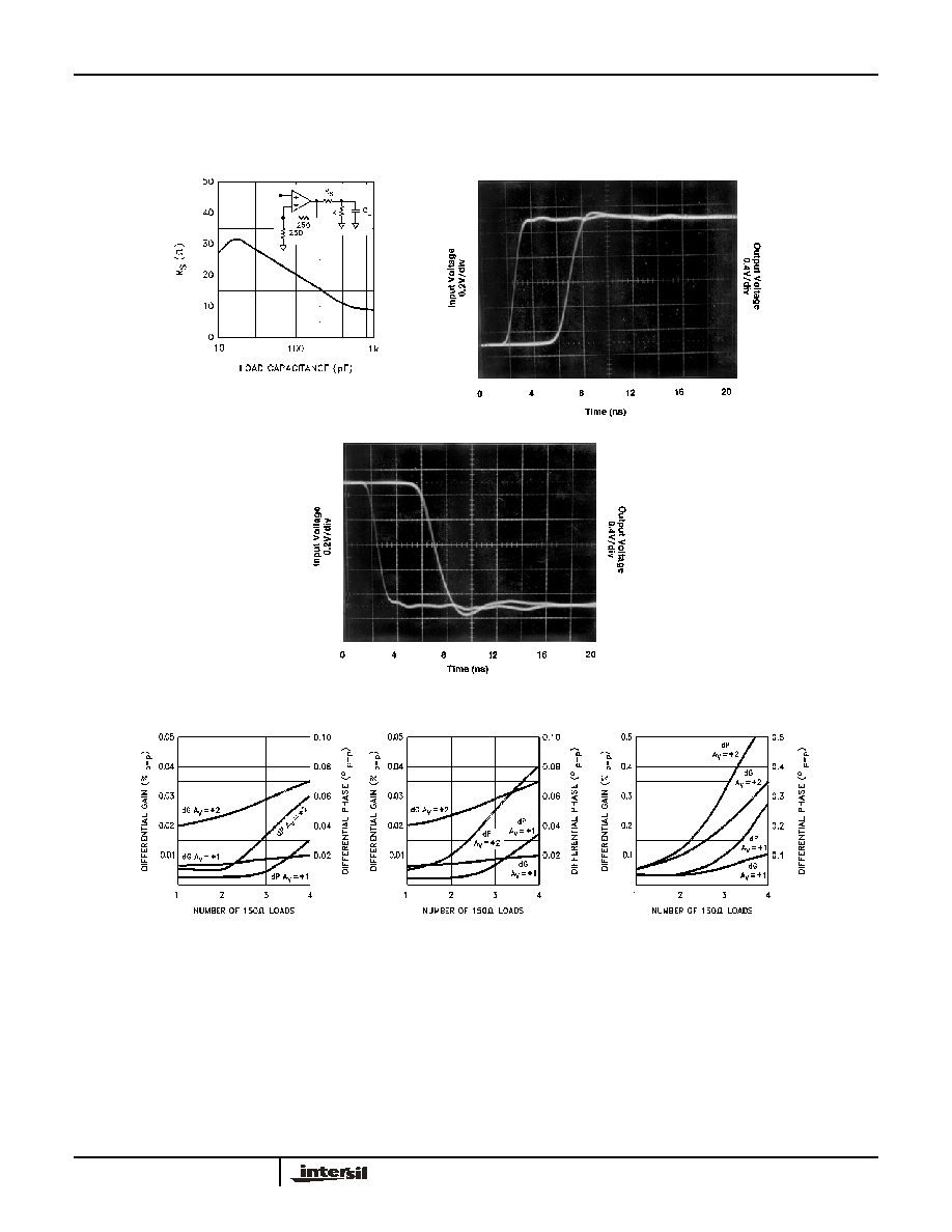
Typical Performance Curves
(Continued)
Differential Gain and
Phase (3.58MHz)
Pulse Response A
V
= +2
Pulse Response A
V
= +2
Differential Gain and
Phase (4.43MHz)
Differential Gain and
Phase (30MHz)
Recommended R
S
vs
Load Capacitance
EL400