 | –≠–Ľ–Ķ–ļ—ā—Ä–ĺ–Ĺ–Ĺ—č–Ļ –ļ–ĺ–ľ–Ņ–ĺ–Ĺ–Ķ–Ĺ—ā: EL4452 | –°–ļ–į—á–į—ā—Ć:  PDF PDF  ZIP ZIP |
1
ģ
FN7170
CAUTION: These devices are sensitive to electrostatic discharge; follow proper IC Handling Procedures.
1-888-INTERSIL or 321-724-7143
|
Intersil (and design) is a registered trademark of Intersil Americas Inc.
Copyright © Intersil Americas Inc. 2003. All Rights Reserved. Elantec is a registered trademark of Elantec Semiconductor, Inc.
All other trademarks mentioned are the property of their respective owners.
EL4452
Wideband Variable-Gain Amplifier with
Gain of 10
The EL4452 is a complete variable-
gain circuit. It offers wide bandwidth
and excellent linearity, while including
a powerful output voltage amplifier, drawing modest current.
The higher gain and lower input noise makes the EL4452
ideal for use in AGC systems.
The EL4452 operates on Ī5V to Ī15V and has an analog
input range of Ī0.5V. AC characteristics do not change
appreciably over the supply range.
The circuit has an operational temperature of -40įC to +85įC
and is packaged in 14-pin PDIP and SO-14.
The EL4452 is fabricated with Elantec's proprietary
complementary bipolar process which gives excellent signal
symmetry and is very rugged.
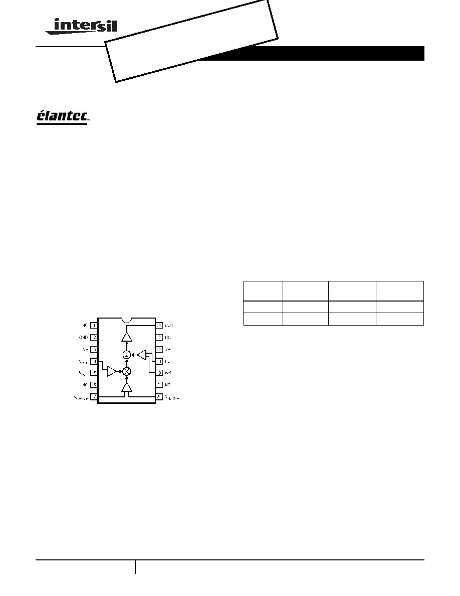
Pinout
Features
∑ Complete variable-gain amplifier complete with output
amplifier
∑ Compensated for Gain
10
∑ 50MHz signal bandwidth
∑ 50MHz gain-control bandwidth
∑ Low 29nV/
Hz input noise
∑ Operates on Ī5V to Ī15V supplies
∑ All inputs are differential
∑ > 70dB attenuation @ 5MHz
Applications
∑ AGC variable-gain amplifier
∑ IF amplifier
∑ Transducer amplifier
EL4452
(14-PIN PDIP, SO)
TOP VIEW
Ordering Information
PART
NUMBER
TEMP. RANGE
PACKAGE
PKG. NO.
EL4452CN
-40įC to +85įC
14-Pin PDIP
MDP0031
EL4452CS
-40įC to +85įC
14-Pin SO
MDP0027
Data Sheet
December 1994, Rev A
OBS
OLE
TE P
ROD
UCT
NO
REC
OMM
END
ED R
EPL
ACE
MEN
T
con
tact
our
Tec
hnic
al S
upp
ort C
ente
r at
1-88
8-IN
TER
SIL
or w
ww.
inter
sil.c
om/
tsc

2
Absolute Maximum Ratings
(T
A
= 25įC)
V+
Positive Supply Voltage . . . . . . . . . . . . . . . . . . . . . . . . . 16.5V
V
S
V+ to V- Supply Voltage . . . . . . . . . . . . . . . . . . . . . . . . . .33V
V
IN
Voltage at any Input or Feedback . . . . . . . . . . . . . . . V+ to V-
V
IN
Difference between Pairs of Inputs or Feedback. . . . . . . . .6V
I
IN
Current into any Input or Feedback Pin. . . . . . . . . . . . . . 4mA
I
OUT
Output Current . . . . . . . . . . . . . . . . . . . . . . . . . . . . . . . 30mA
P
D
Maximum Power Dissipation . . . . . . . . . . . . . . . . See Curves
T
A
Operating Temperature Range . . . . . . . . . . . . -40įC to +85įC
T
S
Storage Temperature Range. . . . . . . . . . . . . -60įC to +150įC
CAUTION: Stresses above those listed in "Absolute Maximum Ratings" may cause permanent damage to the device. This is a stress only rating and operation of the
device at these or any other conditions above those indicated in the operational sections of this specification is not implied.
IMPORTANT NOTE: All parameters having Min/Max specifications are guaranteed. Typical values are for information purposes only. Unless otherwise noted, all tests
are at the specified temperature and are pulsed tests, therefore: T
J
= T
C
= T
A
Open-Loop DC Electrical Specifications
Power supplies at Ī5V, T
A
= 25įC, R
F
= 910
, R
G
= 100
, R
L
= 500
PARAMETER
DESCRIPTION
MIN
TYP
MAX
UNITS
V
DIFF
Signal Input Differential Input Voltage
Clipping
0.4
0.5
V
0.6% Nonlinearity
0.4
V
V
CM
Common-Mode Range (All Inputs; V
DIFF
= 0) V
S
= Ī5V
Ī2.0
Ī2.8
V
V
S
= Ī15V
Ī12.0
Ī12.8
V
V
OS
Input Offset Voltage
10
mV
V
OS
, FB
Output Offset Voltage
10
mV
V
G
, 100%
Extrapolated Voltage for 100% Gain
1.8
2.1
2.2
V
V
G
, 0%
Extrapolated Voltage for 0% Gain
-0.16
-0.06
0.04
V
V
G
, 1V
Gain at V
GAIN
= 1 (R
F
= 910
, R
G
= 100
)
4.9
5.35
5.9
V/V
I
B
Input Bias Current (All Inputs)
-20
-9
0
ĶA
I
OS
Input Offset Current Between V
IN
+ and V
IN
-, V
GAIN
+ and V
GAIN
-
0.5
4
ĶA
F
T
Signal Feedthrough, V
G
= -1V
-100
-70
dB
R
IN
, Signal
Input Resistance, Signal Input
25
60
k
R
IN
, Gain
Input Resistance, Gain Input
50
120
k
R
IN
, FB
Input Resistance, Feedback
25
60
k
CMRR
Common-Mode Rejection Ratio, V
IN
70
90
dB
PSRR
Power-Supply Rejection Ratio, V
OS
, FB; Supplies from Ī5V to Ī15V
65
83
dB
E
G
Gain Error, Excluding Feedback Resistors, V
GAIN
= 2.5V
-7
+7
%
NL
Nonlinearity, V
IN
from -0.25V to +0.25, V
GAIN
= 1V
0.3
0.6
%
V
O
Output Voltage Swing (V
IN
= 0, V
REF
Varied)
V
S
= Ī5V
Ī2.5
Ī2.8
V
V
S
= Ī15V
Ī12.5
Ī12.8
V
I
SC
Output Short-Circuit Current
40
85
mA
I
S
Supply Current, V
S
= Ī15V
15.5
18
mA
EL4452

3
Test Circuit
Closed-Loop AC Electrical Specifications
Power supplies at Ī12V, T
A
= 25įC, R
L
= 500
, C
L
= 15pF
PARAMETER
DESCRIPTION
MIN
TYP
MAX
UNITS
BW, -3dB
-3dB Small-Signal Bandwidth, Signal Input
50
MHz
BW, Ī0.1dB
0.1dB Flatness Bandwidth, Signal Input
10
MHz
Peaking
Frequency Response Peaking
0.1
dB
BW, Gain
-3dB Small-Signal Bandwidth, Gain Input
50
MHz
SR
Slew Rate, V
OUT
between -2V and +2V
350
400
550
V/Ķs
V
N
Input-Referred Noise Voltage Density
29
nV/rt
Hz
Note: For typical performance curves, R
F
= 910
, R
G
= 100
, V
GAIN
= 1V,
R
L
= 500
, and C
L
= 15pF unless otherwise noted.
EL4452

4
Typical Performance Curves
Frequency Response for Various
Feedback Divider Ratios
Frequency Response for
Various Gains
Frequency Response for
Various R
L
, C
L
, V
S
= Ī5V
Frequency Response for
Various R
L
, C
L
, V
S
= Ī15V
-3dB Bandwidth vs. Supply Voltage
-3dB Bandwidth vs. Die
Temperature
EL4452
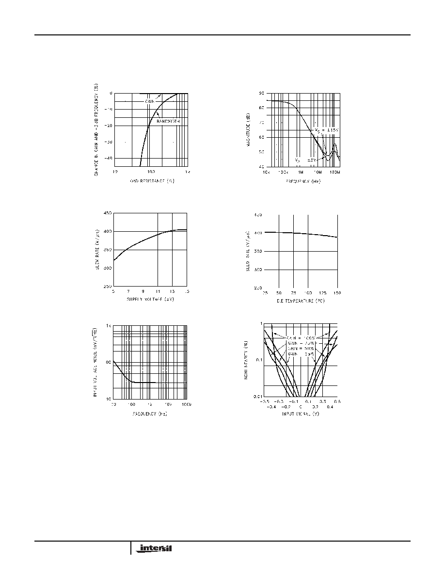
5
Typical Performance Curves
(Continued)
Gain and -3dB Bandwidth vs.
Load Resistance
Input Common-Mode Rejection
Ratio vs. Frequency
Slew Rate vs. Supply Voltage
Slew Rate vs. Die Temperature
Nonlinearity vs. Input Signal
Input Voltage Noise vs. Frequency
EL4452