 | ÐлекÑÑоннÑй компоненÑ: EL5367 | СкаÑаÑÑ:  PDF PDF  ZIP ZIP |
Äîêóìåíòàöèÿ è îïèñàíèÿ www.docs.chipfind.ru
1
®
FN7457.1
CAUTION: These devices are sensitive to electrostatic discharge; follow proper IC Handling Procedures.
1-888-INTERSIL or 321-724-7143
|
Intersil (and design) is a registered trademark of Intersil Americas Inc.
Copyright © Intersil Americas Inc. 2002-2004. All Rights Reserved. Elantec is a registered trademark of Elantec Semiconductor, Inc.
All other trademarks mentioned are the property of their respective owners.
EL5367
1GHz Triple Current Feedback Amplifier
The EL5367 triple amplifier is of the current feedback variety
and exhibits a very high bandwidth of 1GHz at A
V
= +1 and
800MHz at A
V
= +2. This makes this amplifier ideal for
today's high speed video and monitor applications, as well
as a number of RF and IF frequency designs.
With a total supply current of just 25mA and the ability to run
from a single supply voltage from 5V to 12V, this amplifier
offers very high performance for little power consumption.
The EL5367 is available in a 16-pin QSOP package and is
specified for operation over the full -40°C to +85°C
temperature range.
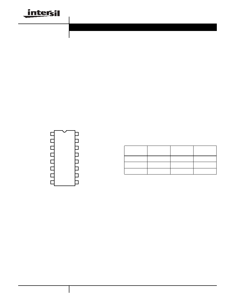
Pinout
EL5367
(16-PIN QSOP)
TOP VIEW
Features
· Gain-of-1 bandwidth = 1GHz
· Gain-of-2 bandwidth = 800MHz
· 6000V/µs slew rate
· Single and dual supply operation from 5V to 12V
· Low noise = 1.7nV/
Hz
· 8.5mA supply current
Applications
· Video amplifiers
· Cable drivers
· RGB amplifiers
· Test equipment
· Instrumentation
· Current-to-voltage converters
1
2
3
4
16
15
14
13
5
6
7
12
11
10
8
9
INMA
VSMA
INPA
VSMB
GND
INPB
VSMC
INPC
VSPA
OUTA
INMB
VSPB
OUTB
INMC
VSPC
OUTC
Ordering Information
PART
NUMBER
PACKAGE
TAPE & REEL
PKG. DWG. #
EL5367IU
16-Pin QSOP
-
MDP0040
EL5367IU-T7
16-Pin QSOP
7"
MDP0040
EL5367IU-T13
16-Pin QSOP
13"
MDP0040
Data Sheet
November 9, 2004
2
FN7457.1
November 9, 2004
Absolute Maximum Ratings
(T
A
= 25°C)
Supply Voltage between V
S
+ and V
S
- . . . . . . . . . . . . . . . . . . . 13.2V
Maximum Continuous Output Current . . . . . . . . . . . . . . . . . . . 50mA
I
OUT
. . . . . . . . . . . . . . . . . . . . . . . . . . . . . . . . . . . . . . . . . . . ±200mA
I into V
IN
+, V
IN
- . . . . . . . . . . . . . . . . . . . . . . . . . . . . . . . . . . . . ±4mA
Power Dissipation . . . . . . . . . . . . . . . . . . . . . . . . . . . . . See Curves
Pin Voltages. . . . . . . . . . . . . . . . . . . . . . . . . V
S
- -0.5V to V
S
+ +0.5V
Storage Temperature . . . . . . . . . . . . . . . . . . . . . . . .-65°C to +150°C
Ambient Operating Temperature . . . . . . . . . . . . . . . .-40°C to +85°C
Die Junction Temperature . . . . . . . . . . . . . . . . . . . . . . . . . . . +125°C
CAUTION: Stresses above those listed in "Absolute Maximum Ratings" may cause permanent damage to the device. This is a stress only rating and operation of the
device at these or any other conditions above those indicated in the operational sections of this specification is not implied.
IMPORTANT NOTE: All parameters having Min/Max specifications are guaranteed. Typical values are for information purposes only. Unless otherwise noted, all tests
are at the specified temperature and are pulsed tests, therefore: T
J
= T
C
= T
A
Electrical Specifications
V
S
+ = +5V, V
S
- = -5V, R
F
= 392
for A
V
= 1, R
F
= 250
for A
V
= 2, R
L
= 150
, T
A
= 25°C, unless otherwise
specified.
PARAMETER
DESCRIPTION
CONDITIONS
MIN
TYP
MAX
UNIT
AC PERFORMANCE
BW
-3dB Bandwidth (per channel)
A
V
= +1
1000
MHz
A
V
= +2
800
MHz
BW1
0.1dB Bandwidth (per channel)
A
V
= +2
100
MHz
SR
Slew Rate
V
O
= -2.5V to +2.5V, A
V
= +2
3000
6000
V/µs
t
S
0.1% Settling Time
V
OUT
= -2.5V to +2.5V, A
V
= -1
8
ns
e
N
Input Voltage Noise
1.7
nV/
Hz
i
N
-
IN- Input Current Noise
19
pA/
Hz
i
N
+
IN+ Input Current Noise
50
pA/
Hz
dG
Differential Gain Error (Note 1)
0.01
%
dP
Differential Phase Error (Note 1)
0.03
°
DC PERFORMANCE
V
OS
Offset Voltage
-5
-0.5
5
mV
T
C
V
OS
Input Offset Voltage Temperature
Coefficient
Measured from T
MIN
to T
MAX
3.52
µV/°C
R
OL
Transimpedance
0.5
1.1
2.5
M
INPUT CHARACTERISTICS
CMIR
Common Mode Input Range
(guaranteed by CMRR test)
±3
±3.3
V
CMRR
Common Mode Rejection Ratio
52
57
66
dB
-ICMR
- Input Current Common Mode Rejection
0
0.7
1
µA/V
+I
IN
+ Input Current
-25
0.7
25
µA
-I
IN
- Input Current
-25
8.5
25
µA
R
IN
Input Resistance
50
130
250
k
C
IN
Input Capacitance
1.5
pF
OUTPUT CHARACTERISTICS
V
O
Output Voltage Swing
R
L
= 150
to GND
±3.6
±3.8
±4.1
V
R
L
= 1k
to GND
±3.8
±4.0
±4.2
V
I
OUT
Output Current
R
L
= 10
to GND
±110
±160
±200
mA
EL5367
3
FN7457.1
November 9, 2004
SUPPLY
I
S
Supply Current - Enabled
No load, V
IN
= 0V
7.5
8.5
9.3
mA
PSRR
Power Supply Rejection Ratio
DC, V
S
= ±4.75V to ±5.25V
70
50
dB
-IPSR
- Input Current Power Supply Rejection
DC, V
S
= ±4.75V to ±5.25V
-0.5
0.2
1
µA/V
NOTE:
1. Standard NTSC test, AC signal amplitude = 286mV, f = 3.58MHz.
Electrical Specifications
V
S
+ = +5V, V
S
- = -5V, R
F
= 392
for A
V
= 1, R
F
= 250
for A
V
= 2, R
L
= 150
, T
A
= 25°C, unless otherwise
specified. (Continued)
PARAMETER
DESCRIPTION
CONDITIONS
MIN
TYP
MAX
UNIT
EL5367
4
FN7457.1
November 9, 2004
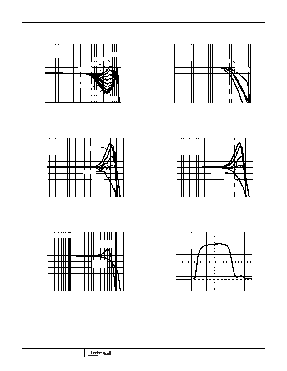
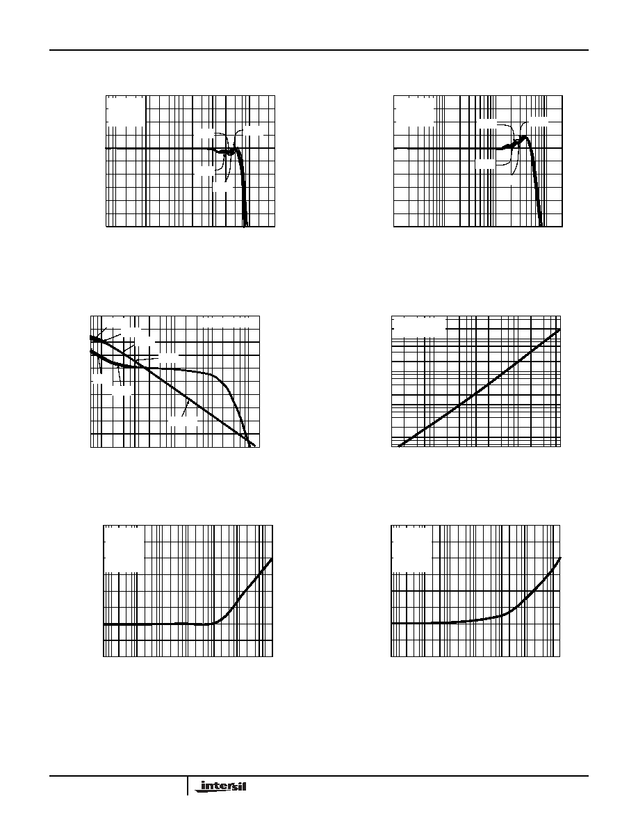
Typical Performance Curves
FIGURE 1. FREQUENCY RESPONSE AS THE FUNCTION OF
R
F
FIGURE 2. FREQUENCY RESPONSE AS THE FUNCTION OF
THE GAIN
FIGURE 3. FREQENCY RESPONSE vs C
IN
FIGURE 4. NON-INVERTING FREQUENCY RESPONSE FOR
VARIOUS C
IN
-
FIGURE 5. INVERTING FREQUENCY RESPONSE FOR GAIN
OF 1 AND 2
FIGURE 6. RISE AND FALL TIME
NORMALIZ
E
D
MAGNITUDE
(dB
)
100K
FREQUENCY (Hz)
V
CC
=5V
V
EE
=-5V
R
L
=150
1M
10M
100M
1G
5
3
1
-1
-3
-5
R
F
=511
R
F
=608
R
F
=368
R
F
=392
R
F
=662
R
F
=1K
R
F
=806
R
F
=900
R
F
=698
V
CC
=5V
V
EE
=-5V
R
L
=150
R
F
=392
R
G
=392
R
G
=43
R
G
=93
R
G
=186
NORMALIZ
E
D
MAGNITUDE
(dB
)
100K
FREQUENCY (Hz)
1M
10M
100M
1G
4
2
0
-2
-4
-6
V
CC
=+5V
V
EE
=-5V
R
L
=150
R
F
=392
C=4.7pF
C=0pF
C=1pF
C=1.5pF
C=2.5pF
NORMALIZ
E
D
MAGN
ITUDE
(dB)
5
3
1
-1
-3
-5
100K
FREQUENCY (Hz)
1M
10M
100M
1G
V
CC
=+5V
V
EE
=-5V
R
L
=150
R
F
=R
G
=392
NORMALIZ
E
D
MAGN
ITUDE
(dB)
5
3
1
-1
-3
-5
100K
FREQUENCY (Hz)
1M
10M
100M
1G
C=4.7pF
C=0pF
C=1pF
C=1.5pF
C=2.5pF
R
F
=220
R
G
=220
V
CC
, V
EE
=5V
R
F
=220
R
G
=100
NOR
M
ALIZED MAGNITUDE
(dB)
4
2
0
-2
-4
-6
1M
FREQUENCY (Hz)
10M
100M
1G
0.5V/DIV
2ns/DIV
V
CC
=+5V
V
EE
=-5V
R
L
=150
R
F
=392
EL5367
5
FN7457.1
November 9, 2004
FIGURE 7. FREQUENCY RESPONSE AS THE FUNCTION OF
THE POWER SUPPLY VOLTAGE
FIGURE 8. INVERTING AMPLIFIER, FREQUENCY
RESPONSE AS THE FUNCTION OF V
CC
, V
EE
GAIN - 1
FIGURE 9. TRANSIMPEDANCE MAGNITUDE AND PHASE AS
THE FUNCTION OF THE FREQUENCY
FIGURE 10. CLOSED LOOP OUTPUT IMPEDANCE vs
FREQUENCY
FIGURE 11. PSRR +5V
FIGURE 12. PSRR -5V
Typical Performance Curves
(Continued)
R
L
=150
R
F
=300
R
G
=300
2.5V
3.0V
6.0V
5.0V
NORMALIZED MAGNIT
UDE
(dB)
4
2
0
-2
-4
-6
100K
FREQUENCY (Hz)
1M
10M
100M
1G
R
L
=150
R
F
=220
R
G
=220
5.0V
6.0V
2.5V
3.5V
NORMALIZED MAGNIT
UDE
(dB)
4
2
0
-2
-4
-6
1M
FREQUENCY (Hz)
10M
100M
1G
ROL (
)
100K
FREQUENCY (Hz)
1M
10M
100M
1G
V
CC
, V
EE
=2.5V
2.5V
5.0V
6.0V
2.5V
5.0V
1M
100K
10K
1K
100
45
-45
-135
-225
-315
PHASE (°
)
ROL
PHASE
V
CC
, V
EE
=5V
GAIN=2
10K
FREQUENCY (Hz)
100K
1M
10M
100M
OUTPUT IMPDEANCE
(
)
10
1
100m
10m
V
CC
=5V
V
EE
=-5V
R
L
=150
R
F
=402
R
G
=402
100
FREQUENCY (Hz)
1K
10K
1M
100M
PSRR (V
CC
) (dB)
0
10
30
50
70
80
20
40
60
100K
10M
V
CC
=5V
V
EE
=-5V
R
L
=150
R
F
=402
R
G
=402
100
FREQUENCY (Hz)
1K
10K
1M
100M
PS
RR
(V
EE
) (dB)
0
10
30
50
70
80
20
40
60
100K
10M
EL5367