 | –≠–ª–µ–∫—Ç—Ä–æ–Ω–Ω—ã–π –∫–æ–º–ø–æ–Ω–µ–Ω—Ç: HFA3102 | –°–∫–∞—á–∞—Ç—å:  PDF PDF  ZIP ZIP |
3-449
HFA3102
Dual Long-Tailed Pair Transistor Array
The HFA3102 is an all NPN transistor array configured as
dual differential amplifiers with tail transistors. Based on
Intersil bonded wafer UHF-1 SOI process, this array
achieves very high f
T
(10GHz) while maintaining excellent
h
FE
and V
BE
matching characteristics over temperature.
Collector leakage currents are maintained to under 0.01nA.
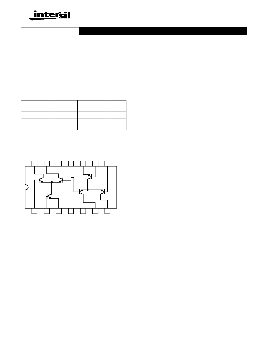
Pinout/Functional Diagram
HFA3102
(SOIC)
TOP VIEW
Features
∑ High Gain-Bandwidth Product (f
T
) . . . . . . . . . . . . . 10GHz
∑ High Power Gain-Bandwidth Product . . . . . . . . . . . . 5GHz
∑ High Current Gain (h
FE
) . . . . . . . . . . . . . . . . . . . . . . . 70
∑ Noise Figure (Transistor) . . . . . . . . . . . . . . . . . . . . . 3.5dB
∑ Low Collector Leakage Current . . . . . . . . . . . . . <0.01nA
∑ Excellent h
FE
and V
BE
Matching
∑ Pin-to-Pin to UPA102G
Applications
∑ Single Balanced Mixers
∑ Wide Band Amplification Stages
∑ Differential Amplifiers
∑ Multipliers
∑ Automatic Gain Control Circuits
∑ Frequency Doublers, Tripplers
∑ Oscillators
∑ Constant Current Sources
∑ Wireless Communication Systems
∑ Radio and Satellite Communications
∑ Fiber Optic Signal Processing
∑ High Performance Instrumentation
Ordering Information
PART NUMBER
TEMP.
RANGE (
o
C)
PACKAGE
PKG.
NO.
HFA3102B
-40 to 85
14 Ld SOIC
M14.15
HFA3102B96
-40 to 85
14 Ld SOIC Tape
and Reel
M14.15
1
2
3
4
5
6
7
14
13
12
11
10
9
8
Q
1
Q
2
Q
3
Q
4
Q
5
Q
6
Data Sheet
August 1996
File Number
3635.2
CAUTION: These devices are sensitive to electrostatic discharge; follow proper IC Handling Procedures.
1-888-INTERSIL or 321-724-7143
|
Copyright
©
Intersil Corporation 1999
3-450
Absolute Maximum Ratings
T
A
= 25
o
C
Thermal Information
V
CEO
Collector to Emitter Voltage . . . . . . . . . . . . . . . . . . . . . . . 8.0V
V
CBO
Collector to Base Voltage . . . . . . . . . . . . . . . . . . . . . . . 12.0V
V
EBO
Emitterr to Base Voltage . . . . . . . . . . . . . . . . . . . . . . . . 12.0V
I
C
, Collector Current . . . . . . . . . . . . . . . . . . . . . . . . . . . . . . . . 30mA
Operating Conditions
Temperature Range . . . . . . . . . . . . . . . . . . . . . . . . . . -40
o
C to 85
o
C
Thermal Resistance (Typical, Note 1)
JA
(
o
C/W)
SOIC Package . . . . . . . . . . . . . . . . . . . . . . . . . . . . .
125
Maximum Power Dissipation at 75
o
C
Any One Transistor. . . . . . . . . . . . . . . . . . . . . . . . . . . . . . . .0.25W
Maximum Junction Temperature (Die) . . . . . . . . . . . . . . . . . . . .175
o
C
Maximum Junction Temperature (Plastic Package) . . . . . . . .150
o
C
Maximum Storage Temperature Range . . . . . . . . . . -65
o
C to 150
o
C
Maximum Lead Temperature (Soldering 10s) . . . . . . . . . . . . .300
o
C
(SOIC - Lead Tips Only)
CAUTION: Stresses above those listed in "Absolute Maximum Ratings" may cause permanent damage to the device. This is a stress only rating and operation of the
device at these or any other conditions above those indicated in the operational sections of this specification is not implied.
NOTE:
1.
JA
is measured with the component mounted on an evaluation PC board in free air.
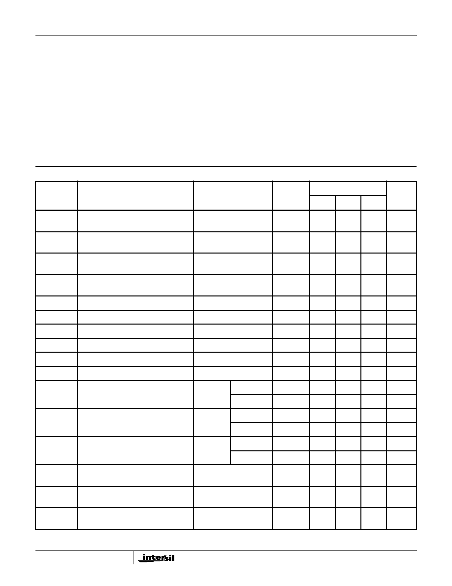
Electrical Specifications
T
A
= 25
o
C
SYMBOLS
PARAMETER
TEST CONDITIONS
(NOTE 2)
TEST
LEVEL
ALL GRADES
UNITS
MIN
TYP
MAX
V
(BR)CBO
Collector-to-Base Breakdown Voltage
(Q
1
, Q
2
, Q
4
, and Q
5
)
I
C
= 100
µ
A, I
E
= 0
A
12
18
-
V
V
(BR)CEO
Collector-to-Emitter Breakdown
Voltage (Q
1
thru Q
6
)
I
C
= 100
µ
A, I
B
= 0
A
8
12
-
V
V
(BR)EBO
Emitter-to-Base Breakdown Voltage (Q
3
and Q
6
)
I
E
= 50
µ
A, I
C
= 0
A
5.5
6
-
V
I
CBO
Collector Cutoff Current
(Q
1
, Q
2
, Q
4
, and Q
5
)
V
CB
= 5V, I
E
= 0
A
-
0.1
10
nA
I
EBO
Emitter Cutoff Current (Q
3
and Q
6
)
V
EB
= 1V, I
C
= 0
A
-
-
100
nA
h
FE
DC Current Gain (Q
1
thru Q
6
)
I
C
= 10mA, V
CE
= 3V
A
40
70
-
-
C
CB
Collector-to-Base Capacitance
V
CB
= 5V, f = 1MHz
B
-
300
-
fF
C
EB
Emitter-to-Base Capacitance
V
EB
= 0, f = 1MHz
B
-
200
-
fF
f
T
Current Gain-Bandwidth Product
I
C
= 10mA, V
CE
= 5V
C
-
10
-
GHz
f
MAX
Power Gain
-
Bandwidth Product
I
C
= 10mA, V
CE
= 5V
C
-
5
-
GHz
G
NFMIN
Available Gain at Minimum Noise Figure
I
C
= 3mA,
V
CE
= 3V
f = 0.5GHz
C
-
17.5
-
dB
f = 1.0GHz
C
-
12.4
-
dB
NF
MIN
Minimum Noise Figure
I
C
= 3mA,
V
CE
= 3V
f = 0.5GHz
C
-
1.8
-
dB
f = 1.0GHz
C
-
2.1
-
dB
NF
50
50
Noise Figure
I
C
= 3mA,
V
CE
= 3V
f = 0.5GHz
C
-
3.3
-
dB
f = 1.0GHz
C
-
3.5
-
dB
h
FE1
/h
FE2
DC Current Gain Matching
(Q
1
and Q
2
, Q
4
and Q
5
)
I
C
= 10mA, V
CE
= 3V
A
0.9
1.0
1.1
-
V
OS
Input Offset Voltage (Q
1
and Q
2
),
(Q
4
and Q
5
)
I
C
= 10mA, V
CE
= 3V
A
-
1.5
5
mV
I
OS
Input Offset Current (Q
1
and Q
2
),
(Q
4
and Q
5
)
I
C
= 10mA, V
CE
= 3V
A
-
5
25
µ
A
HFA3102

3-451
PSPICE Model for a Single Transistor
.Model NUHFARRY NPN
+ ( IS= 1.840E-16 XTI= 3.000E+00 EG= 1.110E+00 VAF= 7.200E+01
+ VAR= 4.500E+00 BF= 1.036E+02 ISE= 1.686E-19 NE= 1.400E+00
+ IKF= 5.400E-02 XTB= 0.000E+00 BR= 1.000E+01 ISC= 1.605E-14
+ NC= 1.800E+00 IKR= 5.400E-02 RC= 1.140E+01 CJC= 3.980E-13
+ MJC= 2.400E-01 VJC= 9.700E-01 FC= 5.000E-01 CJE= 2.400E-13
+ MJE= 5.100E-01 VJE= 8.690E-01 TR= 4.000E-09 TF= 10.51E-12
+ ITF= 3.500E-02 XTF= 2.300E+00 VTF= 3.500E+00 PTF= 0.000E+00
+ XCJC= 9.000E-01 CJS= 1.689E-13 VJS= 9.982E-01 MJS= 0.000E+00
+ RE= 1.848E+00 RB= 5.007E+01 RBM= 1.974E+00 KF= 0.000E+00
+ AF= 1.000E+00)
dV
OS
/dT
Input Offset Voltage TC
(Q
1
and Q
2
, Q
4
and Q
5
)
I
C
= 10mA, V
CE
= 3V
C
-
0.5
-
µ
V/
o
C
I
TRENCH-
LEAKAGE
Collector-to-Collector Leakage
(Pin 6, 7, 13, and 14)
V
TEST
= 5V
B
-
0.01
-
nA
NOTE:
2. Test Level: A. Production Tested; B. Typical or Guaranteed Limit Based on Characterization; C. Design Typical for Information Only
Electrical Specifications
T
A
= 25
o
C (Continued)
SYMBOLS
PARAMETER
TEST CONDITIONS
(NOTE 2)
TEST
LEVEL
ALL GRADES
UNITS
MIN
TYP
MAX
HFA3102

3-452
Common Emitter S-Parameters
V
CE
= 5V and I
C
= 5mA
V
CE
= 5V and I
C
= 10mA
FREQ. (Hz)
|S
11
|
PHASE(S
11
)
|S
12
|
PHASE(S
12
)
|S
21
|
PHASE(S
21
)
|S
22
|
PHASE(S
22
)
1.0E+08
0.833079
-11.7873
1.418901E-02
78.8805
11.0722
168.576
0.976833
-11.0509
2.0E+08
0.791776
-22.8290
2.695740E-02
68.6355
10.5177
157.897
0.930993
-21.3586
3.0E+08
0.734911
-32.6450
3.750029E-02
59.5861
9.75379
148.443
0.868128
-30.4451
4.0E+08
0.672811
-41.0871
4.572138E-02
51.9018
8.91866
140.361
0.799886
-38.1641
5.0E+08
0.612401
-48.2370
5.194147E-02
45.5043
8.10511
133.569
0.734033
-44.5998
6.0E+08
0.557126
-54.2780
5.659943E-02
40.2112
7.35944
127.882
0.674392
-49.9370
7.0E+08
0.508133
-59.4102
6.009507E-02
35.8226
6.69712
123.102
0.622181
-54.3777
8.0E+08
0.465361
-63.8123
6.274213E-02
32.1594
6.11750
119.047
0.577269
-58.1022
9.0E+08
0.428238
-67.6313
6.477134E-02
29.0743
5.61303
115.571
0.538952
-61.2587
1.0E+09
0.396034
-70.9834
6.634791E-02
26.4506
5.17405
112.556
0.506365
-63.9647
1.1E+09
0.368032
-73.9591
6.758932E-02
24.1974
4.79104
109.913
0.478663
-66.3116
1.2E+09
0.343589
-76.6285
6.857937E-02
22.2441
4.45546
107.570
0.455091
-68.3702
1.3E+09
0.322155
-79.0462
6.937837E-02
20.5358
4.15997
105.472
0.435008
-70.1958
1.4E+09
0.303268
-81.2548
7.003020E-02
19.0293
3.89845
103.576
0.417872
-71.8314
1.5E+09
0.286542
-83.2880
7.056718E-02
17.6908
3.66577
101.849
0.403238
-73.3108
1.6E+09
0.271660
-85.1723
7.101343E-02
16.4930
3.45770
100.262
0.390735
-74.6609
1.7E+09
0.258359
-86.9292
7.138717E-02
15.4143
3.27074
98.7956
0.380056
-75.9030
1.8E+09
0.246420
-88.5759
7.170231E-02
14.4370
3.10197
97.4307
0.370947
-77.0544
1.9E+09
0.235659
-90.1265
7.196964E-02
13.5469
2.94897
96.1533
0.363195
-78.1288
2.0E+09
0.225923
-91.5925
7.219757E-02
12.7319
2.80969
94.9515
0.356623
-79.1377
2.1E+09
0.217085
-92.9836
7.239274E-02
11.9824
2.68243
93.8156
0.351081
-80.0903
2.2E+09
0.209034
-94.3076
7.256046E-02
11.2901
2.56573
92.7373
0.346442
-80.9942
2.3E+09
0.201678
-95.5713
7.270498E-02
10.6480
2.45837
91.7097
0.342599
-81.8557
2.4E+09
0.194939
-96.7803
7.282977E-02
10.0503
2.35928
90.7271
0.339458
-82.6802
2.5E+09
0.188747
-97.9395
7.293764E-02
9.49212
2.26756
89.7844
0.336942
-83.4719
2.6E+09
0.183044
-99.0530
7.303093E-02
8.96908
2.18243
88.8775
0.334982
-84.2347
2.7E+09
0.177780
-100.124
7.311157E-02
8.47753
2.10322
88.0026
0.333518
-84.9716
2.8E+09
0.172909
-101.156
7.318117E-02
8.01430
2.02934
87.1565
0.332499
-85.6853
2.9E+09
0.168394
-102.152
7.324107E-02
7.57661
1.96027
86.3366
0.331879
-86.3781
3.0E+09
0.164200
-103.114
7.329243E-02
7.16204
1.89556
85.5404
0.331620
-87.0518
FREQ. (Hz)
|S
11
|
PHASE(S
11
)
|S
12
|
PHASE(S
12
)
|S
21
|
PHASE(S
21
)
|S
22
|
PHASE(S
22
)
1.0E+08
0.728106
-16.4319
1.273920E-02
75.4177
15.1273
165.227
0.959692
-14.2688
2.0E+08
0.670836
-31.2669
2.342300E-02
62.8941
13.9061
152.045
0.886232
-26.9507
3.0E+08
0.600268
-43.7663
3.132521E-02
52.5891
12.3970
141.185
0.796016
-37.3172
4.0E+08
0.531768
-54.0028
3.681579E-02
44.5019
10.9257
132.570
0.708892
-45.4503
5.0E+08
0.471795
-62.3880
4.057046E-02
38.2308
9.62995
125.781
0.633146
-51.7704
6.0E+08
0.421506
-69.3569
4.316292E-02
33.3405
8.53559
120.378
0.570209
-56.7206
7.0E+08
0.379961
-75.2612
4.499071E-02
29.4764
7.62375
116.005
0.518803
-60.6598
8.0E+08
0.345693
-80.3608
4.631140E-02
26.3755
6.86423
112.398
0.476987
-63.8540
9.0E+08
0.317301
-84.8420
4.728948E-02
23.8481
6.22797
109.365
0.442915
-66.4948
1.0E+09
0.293608
-88.8381
4.803091E-02
21.7581
5.69057
106.771
0.415044
-68.7193
1.1E+09
0.273680
-92.4452
4.860515E-02
20.0070
5.23257
104.518
0.392146
-70.6269
1.2E+09
0.256782
-95.7336
4.905871E-02
18.5224
4.83873
102.532
0.373261
-72.2899
1.3E+09
0.242344
-98.7555
4.942344E-02
17.2505
4.49716
100.759
0.357640
-73.7620
1.4E+09
0.229918
-101.551
4.972158E-02
16.1506
4.19854
99.1602
0.344698
-75.0832
1.5E+09
0.219152
-104.150
4.996903E-02
15.1915
3.93554
97.7028
0.333974
-76.2840
1.6E+09
0.209767
-106.577
5.017730E-02
14.3490
3.70234
96.3629
0.325102
-77.3877
1.7E+09
0.201539
-108.851
5.035491E-02
13.6040
3.49428
95.1215
0.317789
-78.4122
1.8E+09
0.194288
-110.988
5.050825E-02
12.9411
3.30758
93.9633
0.311800
-79.3715
1.9E+09
0.187867
-113.001
5.064218E-02
12.3482
3.13919
92.8761
0.306940
-80.2768
2.0E+09
0.182157
-114.902
5.076045E-02
11.8151
2.98658
91.8500
0.303051
-81.1365
2.1E+09
0.177056
-116.698
5.086598E-02
11.3338
2.84766
90.8766
0.300003
-81.9578
2.2E+09
0.172484
-118.399
5.096107E-02
10.8974
2.72068
89.9494
0.297686
-82.7460
2.3E+09
0.168370
-120.012
5.104755E-02
10.5001
2.60420
89.0626
0.296007
-83.5057
2.4E+09
0.164656
-121.542
5.112690E-02
10.1373
2.49697
88.2115
0.294889
-84.2405
2.5E+09
0.161293
-122.996
5.120031E-02
9.80479
2.39793
87.3920
0.294266
-84.9533
2.6E+09
0.158239
-124.378
5.126876E-02
9.49919
2.30619
86.6007
0.294081
-85.6466
2.7E+09
0.155458
-125.694
5.133304E-02
9.21750
2.22098
85.8348
0.294285
-86.3223
2.8E+09
0.152919
-126.947
5.139381E-02
8.95716
2.14162
85.0916
0.294836
-86.9822
2.9E+09
0.150595
-128.140
5.145164E-02
8.71595
2.06753
84.3690
0.295696
-87.6275
3.0E+09
0.148463
-129.279
5.150697E-02
8.49194
1.99820
83.6651
0.296834
-88.2595
HFA3102
3-453
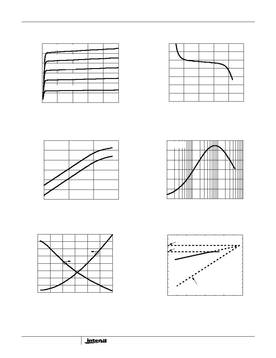
Typical Performance Curves
FIGURE 1. I
C
vs V
CE
FIGURE 2. h
FE
vs I
C
FIGURE 3. GUMMEL PLOT
FIGURE 4. f
T
vs I
C
FIGURE 5. GAIN AND NOISE FIGURE vs FREQUENCY
FIGURE 6. P
1dB
AND 3RD ORDER INTERCEPT
V
CE
(V)
I
C
(mA)
12
10
8
6
4
2
0
0
1
2
3
4
5
I
B
= 150
µ
A
I
B
= 30
µ
A
I
B
= 120
µ
A
I
B
= 60
µ
A
I
B
= 90
µ
A
I
C
(A)
h
FE
0
20
40
60
80
100
120
140
10
-10
10
-8
10
-6
10
-4
10
-2
10
0
V
BE
(V)
I
C
AND I
B
(A)
V
CE
= 3V
10
0
10
-2
10
-4
10
-6
10
-8
10
-10
10
-12
0.4
0.6
0.8
1.0
f
T
(GHz)
I
C
(A)
10
-4
10
-3
10
-2
10
-1
12
10
8
6
4
2
0
V
CE
= 5V
NOISE FIGURE (dB)
FREQUENCY (GHz)
|S
21
| (dB)
4.8
4.6
4.4
4.2
4.0
3.8
3.6
3.4
3.2
0
0.5
1.0
1.5
2.0
2.5
3.0
20
18
14
12
10
8
6
4
16
-30
-20
-10
0
10
-100
-80
-60
-40
-20
0
20
40
V
CE
= 5V
I
C
= 10mA
f = 1GHz
P
IN
, INPUT POWER (dBm)
P
OUT
, OUTPUT PO
WER (dBm)
3RD ORDER PRODUCTS
3rd ORDER INTERCEPT POINT
1dB COMPRESSION POINT
HFA3102