 | ÐлекÑÑоннÑй компоненÑ: HIP4080 | СкаÑаÑÑ:  PDF PDF  ZIP ZIP |
Äîêóìåíòàöèÿ è îïèñàíèÿ www.docs.chipfind.ru
1
December 1996
HIP4080
80V/2.5A Peak, High Frequency
Full Bridge FET Driver
Features
· Drives N-Channel FET Full Bridge Including High Side
Chop Capability
· Bootstrap Supply Max Voltage to 95V
DC
· Drives 1000pF Load at 1MHz in Free Air at 50
o
C with
Rise and Fall Times of 10ns (Typ)
· User-Programmable Dead Time
· Charge-Pump and Bootstrap Maintain Upper Bias
Supplies
· DIS (Disable) Pin Pulls Gates Low
· Input Logic Thresholds Compatible with 5V to 15V
Logic Levels
· Very Low Power Consumption
Applications
· Medium/Large Voice Coil Motors
· Full Bridge Power Supplies
· Class D Audio Power Amplifiers
· High Performance Motor Controls
· Noise Cancellation Systems
· Battery Powered Vehicles
· Peripherals
· U.P.S.
Description
The HIP4080 is a high frequency, medium voltage Full Bridge
N-Channel FET driver IC, available in 20 lead plastic SOIC and
DIP packages. The HIP4080 includes an input comparator,
used to facilitate the "hysteresis" and PWM modes of operation.
Its HEN (high enable) lead can force current to freewheel in the
bottom two external power MOSFETs, maintaining the upper
power MOSFETs off. Since it can switch at frequencies up to
1MHz, the HIP4080 is well suited for driving Voice Coil Motors,
switching amplifiers in class D high-frequency switching audio
amplifiers and power supplies.
HIP4080 can also drive medium voltage brush motors, and
two HIP4080s can be used to drive high performance step-
per motors, since the short minimum "on-time" can provide
fine micro-stepping capability.
Short propagation delays of approximately 55ns maximizes
control loop crossover frequencies and dead-times which
can be adjusted to near zero to minimize distortion, resulting
in precise control of the driven load.
The similar HIP4081 IC allows independent control of all 4
FETs in an Full Bridge configuration.
See also, Application Note AN9324 for the HIP4080.
Similar part, HIP4080A, includes under voltage circuitry
which doesn't require the circuitry shown in Figure 30 of this
data sheet.
Pinout
HIP4080 (PDIP, SOIC)
TOP VIEW
Ordering Information
PART
NUMBER
TEMP.
RANGE (
o
C)
PACKAGE
PKG.
NO.
HIP4080IP
-40 to 85
20 Lead PDIP
E20.3
HIP4080IB
-40 to 85
20 Lead SOIC
M20.3
11
12
13
14
15
16
17
18
20
19
10
9
8
7
6
5
4
3
2
1
BHB
HEN
DIS
V
SS
OUT
IN+
HDEL
IN-
LDEL
AHB
BHO
BLO
BLS
V
DD
BHS
V
CC
ALS
ALO
AHS
AHO
File Number
3178.10
CAUTION: These devices are sensitive to electrostatic discharge; follow proper IC Handling Procedures.
http://www.intersil.com or 407-727-9207
|
Copyright
©
Intersil Corporation 1999
2
Application Block Diagram
Functional Block Diagram
(1/2 HIP4080)
80V
GND
HIP4080
GND
12V
LOAD
HEN
DIS
IN+
IN-
BHO
BHS
BLO
ALO
AHS
AHO
CHARGE
PUMP
V
DD
HEN
DIS
OUT
IN+
IN
_
HDEL
LDEL
V
SS
TURN-ON
DELAY
+
-
TURN-ON
DELAY
DRIVER
DRIVER
AHB
AHO
AHS
V
CC
ALO
ALS
C
BF
TO V
DD
(PIN 16)
C
BS
D
BS
HIGH VOLTAGE BUS
80V
DC
+12V
DC
LEVEL SHIFT
AND LATCH
14
10
11
12
15
13
16
2
3
5
6
7
8
9
4
BIAS
SUPPLY
HIP4080
3
Typical Application (Hysteresis Mode Switching)
6V
80V
12V
12V
DIS
IN
GND
6V
GND
+
-
11
12
13
14
15
16
17
18
20
19
10
9
8
7
6
5
4
3
2
1 BHB
HEN
DIS
V
SS
OUT
IN+
HDEL
IN-
LDEL
AHB
BHO
BLO
BLS
V
DD
BHS
V
CC
ALS
ALO
AHS
AHO
LOAD
HIP4080
4
Absolute Maximum Ratings
Thermal Information
Supply Voltage, V
DD
and V
CC
. . . . . . . . . . . . . . . . . . . -0.3V to 16V
Logic I/O Voltages . . . . . . . . . . . . . . . . . . . . . . . -0.3V to V
DD
+0.3V
Voltage on AHS, BHS . . . . -6.0V (Transient) to 80V (25
o
C to 125
o
C)
Voltage on AHS, BHS . . . . -6.0V (Transient) to 70V (-55
o
C to 125
o
C
Voltage on ALS, BLS . . . . . . . -2.0V (Transient) to +2.0V (Transient)
Voltage on AHB, BHBV
AHS, BHS
-0.3V to V
AHS, BHS
+16VVoltage on
Voltage on ALO, BLO . . . . . . . . . . . . V
ALS, BLS
-0.3V to V
CC
+0.3V
Voltage on AHO, BHO . . . . . . V
AHS, BHS
-0.3V to V
AHB, BHB
+0.3V
Input Current, HDEL and LDEL . . . . . . . . . . . . . . . . . . -5mA to 0mA
Phase Slew Rate . . . . . . . . . . . . . . . . . . . . . . . . . . . . . . . . . . 20V/ns
NOTE: All Voltages relative to pin 4, V
SS
, unless otherwise specified.
Thermal Resistance (Typical, Note 1)
JA
(
o
C/W)
SOIC Package . . . . . . . . . . . . . . . . . . . . . . . . . . . . .
85
PDIP Package . . . . . . . . . . . . . . . . . . . . . . . . . . . . .
75
Maximum Power Dissipation at 85
o
C
SOIC Package . . . . . . . . . . . . . . . . . . . . . . . . . . . . . . . . . . 470mW
DIP Package . . . . . . . . . . . . . . . . . . . . . . . . . . . . . . . . . . . 530mW
Storage Temperature Range . . . . . . . . . . . . . . . . . . -65
o
C to 150
o
C
Operating Max. Junction Temperature . . . . . . . . . . . . . . . . . 125
o
C
Lead Temperature (Soldering 10s) . . . . . . . . . . . . . . . . . . . . 300
o
C
(SOIC - Lead Tips Only)
CAUTION: Stresses above those listed in "Absolute Maximum Ratings" may cause permanent damage to the device. This is a stress only rating and operation
of the device at these or any other conditions above those indicated in the operational sections of this specification is not implied.
NOTE:
1.
JA
is measured with the component mounted on an evaluation PC board in free air.
Operating Conditions
Supply Voltage, V
DD
and V
CC
. . . . . . . . . . . . . . . . . . . +8V to +15V
Voltage on ALS, BLS . . . . . . . . . . . . . . . . . . . . . . . . . -1.0V to +1.0V
Voltage on AHB, BHB . . . . . . . . V
AHS, BHS
+5V to V
AHS, BHS
+15V
Input Current, HDEL and LDEL. . . . . . . . . . . . . . . . -500
µ
A to -50
µ
A
Operating Ambient Temperature Range . . . . . . . . . . .-40
o
C to 85
o
C
Electrical Specifications
V
DD
= V
CC
= V
AHB
= V
BHB
= 12V, V
SS
= V
ALS
= V
BLS
= V
AHS
= V
BHS
= 0V, R
HDEL
= R
LDEL
= 100K,
and T
A
= 25
o
C, Unless Otherwise Specified
PARAMETERS
SYMBOL
TEST CONDITIONS
T
J
= 25
o
C
T
J
= - 40
o
C
TO 125
o
C
UNITS
MIN
TYP
MAX
MIN
MAX
SUPPLY CURRENTS AND CHARGE PUMPS
V
DD
Quiescent Current
I
DD
IN- = 2.5V, Other Inputs = 0V
8
10.5
13
7
14
mA
V
DD
Operating Current
I
DDO
Outputs switching f = 500kHz
9
11
14
8
15
mA
V
CC
Quiescent Current
I
CC
IN- = 2.5V, Other Inputs = 0V,
I
ALO
= I
BLO
= 0
-
25
80
-
100
µ
A
V
CC
Operating Current
I
CCO
f = 500kHz, No Load
1
1.5
2.0
0.8
3
mA
AHB, BHB Quiescent Current -
Qpump Output Current
I
AHB
, I
BHB
IN- = 2.5V, Other Inputs = 0V, I
AHO
=
I
BHO
= 0, V
DD
= V
CC
= V
AHB
=
V
BHB
= 10V
-50
-30
-15
-60
-10
µ
A
AHB, BHB Operating Current
I
AHBO
,
I
BHBO
f = 500kHz, No Load
0.5
0.9
1.3
0.4
1.7
mA
AHS, BHS, AHB, BHB Leakage Current
I
HLK
V
AHS
= V
BHS
= V
AHB
= V
BHB
= 95V
-
0.02
1.0
-
10
µ
A
AHB-AHS, BHB-BHS Qpump
Output Voltage
V
AHB
- V
AHS
V
BHB
- V
BHS
I
AHB
= I
AHB
= 0, No Load
11.5
12.6
14.0
10.5
14.5
V
INPUT COMPARATOR PINS: IN+, IN-, OUT
Offset Voltage
V
OS
Over Common Mode Voltage Range
-10
0
+10
-15
+15
mV
Input Bias Current
I
IB
0
0.5
2
0
4
µ
A
Input Offset Current
I
OS
-1
0
+1
-2
+2
µ
A
Input Common Mode Voltage Range
CMVR
1
-
V
DD
-1.5
1
V
DD
-1.5
V
Voltage Gain
AVOL
10
25
-
10
-
V/mV
OUT High Level Output Voltage
V
OH
IN+ > IN-, I
OH
= -300
µ
A
V
DD
-0.4
-
-
V
DD
- 0.5
-
V
OUT Low Level Output Voltage
V
OL
IN+ < IN-, I
OL
= 300
µ
A
-
-
0.3
-
0.4
V
High Level Output Current
I
OH
V
OUT
=
6V
-9
-7
-4
-11
-2
mA
Low Level Output Current
I
OL
V
OUT
=
6V
8
10
12
5
14
mA
INPUT PINS: DIS
Low Level Input Voltage
V
IL
Full Operating Conditions
-
-
1.0
-
0.8
V
High Level Input Voltage
V
IH
Full Operating Conditions
2.5
-
-
2.7
-
V
Input Voltage Hysteresis
-
35
-
-
-
mV
HIP4080
5
Low Level Input Current
I
IL
V
IN
= 0V, Full Operating Conditions
-130
-100
-75
-135
-65
µ
A
High Level Input Current
I
IH
V
IN
= 5V, Full Operating Conditions
-1
-
+1
-10
+10
µ
A
INPUT PINS: HEN
Low Level Input Voltage
V
IL
Full Operating Conditions
-
-
1.0
-
0.8
V
High Level Input Voltage
V
IH
Full Operating Conditions
2.5
-
-
2.7
-
V
Input Voltage Hysteresis
-
35
-
-
-
mV
Low Level Input Current
I
IL
V
IN
= 0V, Full Operating Conditions
-260
-200
-150
-270
-130
µ
A
High Level Input Current
I
IH
V
IN
= 5V, Full Operating Conditions
-1
-
+1
-10
+10
µ
A
TURN-ON DELAY PINS: LDEL AND HDEL
LDEL, HDEL Voltage
V
HDEL,
V
I
HDEL
= I
LDEL
= -100
µ
A
4.9
5.1
5.3
4.8
5.4
V
GATE DRIVER OUTPUT PINS: ALO, BLO, AHO, AND BHO
Low Level Output Voltage
V
OL
I
OUT
= 100mA
.70
0.85
1.0
0.5
1.1
V
High Level Output Voltage
V
CC
- V
OH
I
OUT
= -100mA
0.8
0.95
1.1
0.5
1.2
V
Peak Pull-up Current
I
O
+
V
OUT
= 0V
1.7
2.6
3.8
1.4
4.1
A
Peak Pull-down Current
I
O
-
V
OUT
= 12V
1.7
2.4
3.3
1.3
3.6
A
Electrical Specifications
V
DD
= V
CC
= V
AHB
= V
BHB
= 12V, V
SS
= V
ALS
= V
BLS
= V
AHS
= V
BHS
= 0V, R
HDEL
= R
LDEL
= 100K,
and T
A
= 25
o
C, Unless Otherwise Specified (Continued)
PARAMETERS
SYMBOL
TEST CONDITIONS
T
J
= 25
o
C
T
J
= - 40
o
C
TO 125
o
C
UNITS
MIN
TYP
MAX
MIN
MAX
Switching Specifications
V
DD
= V
CC
= V
AHB
= V
BHB
= 12V, V
SS
= V
ALS
= V
BLS
= V
AHS
= V
BHS
= 0V, R
HDEL
= R
LDEL
= 10K,
C
L
= 1000pF, and T
A
= 25
o
C, Unless Otherwise Specified
PARAMETERS
SYMBOL
TEST CONDITIONS
T
J
= 25
o
C
T
J
= - 40
o
C
TO 125
o
C
UNITS
MIN
TYP MAX
MIN
MAX
Lower Turn-off Propagation Delay (IN+/IN- to ALO/BLO)
T
LPHL
-
40
70
-
90
ns
Upper Turn-off Propagation Delay (IN+/IN- to AHO/BHO)
T
HPHL
-
50
80
-
110
ns
Lower Turn-on Propagation Delay (IN+/IN- to ALO/BLO)
T
LPLH
R
HDEL
= R
LDEL
= 10K
-
45
70
-
90
ns
Upper Turn-on Propagation Delay (IN+/IN- to AHO/BHO)
T
HPLH
R
HDEL
= R
LDEL
= 10K
-
70
110
-
140
ns
Rise Time
T
r
-
10
25
-
35
ns
Fall Time
T
f
-
10
25
-
35
ns
Turn-on Input Pulse Width
T
PWIN-ON
R
HDEL
= R
LDEL
= 10K
50
-
-
50
-
ns
Turn-off Input Pulse Width
T
PWIN-OFF
R
HDEL
= R
LDEL
= 10K
40
-
-
40
-
ns
Disable Turn-off Propagation Delay
(DIS - Lower Outputs)
T
DISLOW
-
45
75
-
95
ns
Disable Turn-off Propagation Delay
(DIS - Upper Outputs)
T
DISHIGH
-
55
85
-
105
ns
Disable to Lower Turn-on Propagation Delay
(DIS - ALO and BLO)
T
DLPLH
-
35
70
-
90
ns
Refresh Pulse Width (ALO and BLO)
T
REF-PW
160
260
380
140
420
ns
Disable to Upper Enable (DIS - AHO and BHO)
T
UEN
-
335
500
-
550
ns
HEN-AHO, BHO Turn-off, Propagation Delay
T
HEN-PHL
R
HDEL
= R
LDEL
= 10K
-
35
70
-
90
ns
HEN-AHO, BHO Turn-on, Propagation Delay
T
HEN-PLH
R
HDEL
= R
LDEL
= 10K
-
60
90
-
110
ns
TRUTH TABLE
INPUT
OUTPUT
IN+ > IN-
HEN
DIS
ALO
AHO
BLO
BHO
X
X
1
0
0
0
0
1
1
0
0
1
1
0
0
1
0
1
0
0
1
1
0
0
0
0
1
0
0
0
0
1
0
0
0
HIP4080
6
Pin Descriptions
PIN
NUMBER
SYMBOL
DESCRIPTION
1
BHB
B High-side Bootstrap supply. External bootstrap diode and capacitor are required. Connect cathode of boot-
strap diode and positive side of bootstrap capacitor to this pin. Internal charge pump supplies 30
µ
A out of this
pin to maintain bootstrap supply. Internal circuitry clamps the bootstrap supply to approximately 12.8V.
2
HEN
High-side Enable input. Logic level input that when low overrides IN+/IN- (Pins 6 and 7) to put AHO and BHO
drivers (Pins 11 and 20) in low output state. When HEN is high AHO and BHO are controlled by IN+/IN- inputs.
The pin can be driven by signal levels of 0V to 15V (no greater than V
DD
). An internal 100
µ
A pull-up to V
DD
will
hold HEN high, so no connection is required if high-side and low-side outputs are to be controlled by IN+/IN-
inputs.
3
DIS
DISable input. Logic level input that when taken high sets all four outputs low. DIS high overrides all other inputs.
When DIS is taken low the outputs are controlled by the other inputs. The pin can be driven by signal levels of
0V to 15V (no greater than V
DD
). An internal 100
µ
A pull-up to V
DD
will hold DIS high if this pin is not driven.
4
V
SS
Chip negative supply, generally will be ground.
5
OUT
OUTput of the input control comparator. This output can be used for feedback and hysteresis.
6
IN+
Non-inverting input of control comparator. If IN+ is greater than IN- (Pin 7) then ALO and BHO are low level
outputs and BLO and AHO are high level outputs. If IN+ is less than IN- then ALO and BHO are high level out-
puts and BLO and AHO are low level outputs. DIS (Pin 3) high level will override IN+/IN- control for all outputs.
HEN (Pin 2) low level will override IN+/IN- control of AHO and BHO. When switching in four quadrant mode,
dead time in a half bridge leg is controlled by HDEL and LDEL (Pins 8 and 9).
7
IN-
Inverting input of control comparator. See IN+ (Pin 6) description.
8
HDEL
High-side turn-on DELay. Connect resistor from this pin to V
SS
to set timing current that defines the turn-on delay
of both high-side drivers. The low-side drivers turn-off with no adjustable delay, so the HDEL resistor guarantees
no shoot-through by delaying the turn-on of the high-side drivers. HDEL reference voltage is approximately 5.1V.
9
LDEL
Low-side turn-on DELay. Connect resistor from this pin to V
SS
to set timing current that defines the turn-on delay
of both low-side drivers. The high-side drivers turn-off with no adjustable delay, so the LDEL resistor guarantees
no shoot-through by delaying the turn-on of the low-side drivers. LDEL reference voltage is approximately 5.1V.
10
AHB
A High-side Bootstrap supply. External bootstrap diode and capacitor are required. Connect cathode of boot-
strap diode and positive side of bootstrap capacitor to this pin. Internal charge pump supplies 30
µ
A out of this
pin to maintain bootstrap supply. Internal circuitry clamps the bootstrap supply to approximately 12.8V.
11
AHO
A High-side Output. Connect to gate of A High-side power MOSFET.
12
AHS
A High-side Source connection. Connect to source of A High-side power MOSFET. Connect negative side of
bootstrap capacitor to this pin.
13
ALO
A Low-side Output. Connect to gate of A Low-side power MOSFET.
14
ALS
A Low-side Source connection. Connect to source of A Low-side power MOSFET.
15
V
CC
Positive supply to gate drivers. Must be same potential as V
DD
(Pin 16). Connect to anodes of two bootstrap
diodes.
16
V
DD
Positive supply to lower gate drivers. Must be same potential as V
CC
(Pin 15). De-couple this pin to V
SS
(Pin 4).
17
BLS
B Low-side Source connection. Connect to source of B Low-side power MOSFET.
18
BLO
B Low-side Output. Connect to gate of B Low-side power MOSFET.
19
BHS
B High-side Source connection. Connect to source of B High-side power MOSFET. Connect negative side of
bootstrap capacitor to this pin.
20
BHO
B High-side Output. Connect to gate of B High-side power MOSFET.
HIP4080
7
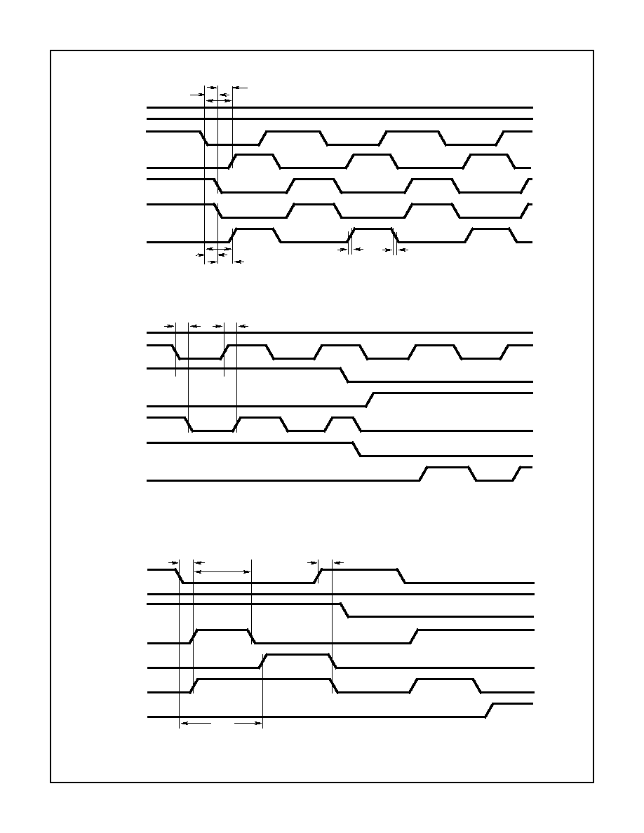
Timing Diagrams
FIGURE 1. BI-STATE MODE
FIGURE 2. HIGH SIDE CHOP MODE
FIGURE 3. DISABLE FUNCTION
HEN = 1
ALO
AHO
BLO
T
LPHL
T
HPLH
T
r
(10% - 90%)
T
f
(90% - 10%)
T
DT
DIS = 0
T
HPHL
T
LPLH
T
DT
IN+ > IN-
BHO
HEN
ALO
AHO
BLO
T
HEN-PLH
T
HEN-PHL
IN+ > IN-
BHO
DIS = 0
HEN = 1
AHO
BLO
DIS
T
REF-PW
T
DLPLH
IN+ > IN-
BHO
T
DIS
T
UEN
ALO
HIP4080
8
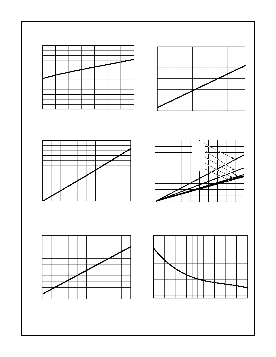
Typical Performance Curves
V
DD
= V
CC
= V
AHB
= V
BHB
= 12V, V
SS
= V
ALS
= V
BLS
= V
AHS
= V
BHS
= 0V,
R
HDEL
= R
LDEL
= 100K, and T
A
= 25
o
C, Unless Otherwise Specified
FIGURE 4. QUIESCENT I
DD
SUPPLY CURRENT vs V
DD
SUPPLY VOLTAGE
FIGURE 5. I
DDO
, NO-LOAD I
DD
SUPPLY CURRENT vs
FREQUENCY (kHz)
FIGURE 6. SIDE A, B FLOATING SUPPLY BIAS CURRENT vs
FREQUENCY (LOAD = 1000pF)
FIGURE 7. I
CCO
, NO-LOAD I
CC
SUPPLY CURRENT vs
FREQUENCY (kHz) TEMPERATURE
FIGURE 8. I
AHB
, I
BHB
, NO-LOAD FLOATING SUPPLY BIAS
CURRENT vs FREQUENCY
FIGURE 9. COMPARATOR INPUT CURRENT I
L
vs
TEMPERATURE AT V
CM
= 5V
8
10
12
14
2.0
4.0
6.0
8.0
10.0
12.0
14.0
I
DD
SUPPL
Y CURRENT (mA)
V
DD
SUPPLY VOLTAGE (V)
13
12.5
12.0
11.5
11.0
10.5
10
200
400
600
800
1000
SUPPL
Y CURRENT (mA)
SWITCHING FREQUENCY (kHz)
0
100
200
300
400
500
600
700
800
900 1000
0.0
5.0
10.0
15.0
20.0
25.0
30.0
FLO
A
TING SUPPL
Y BIAS CURRENT (mA)
SWITCHING FREQUENCY (kHz)
0
100
200
300
400
500
600
700
800
900 1000
0.0
1.0
2.0
3.0
4.0
5.0
I
CC
SUPPL
Y CURRENT (mA)
SWITCHING FREQUENCY (kHz)
75
o
C
25
o
C
125
o
C
-40
o
C
0
o
C
0
200
400
600
800
1000
-0.2
0.2
0.6
1.0
1.4
1.8
FREQUENCY (kHz)
FLO
A
TING SUPPL
Y BIAS CURRENT (mA)
-40
-20
0
20
40
60
80
100
120
0.5
1.0
COMP
ARA
T
OR INPUT CURRENT (
µ
A)
JUNCTION TEMPERATURE (
o
C)
HIP4080
9
FIGURE 10. DIS LOW LEVEL INPUT CURRENT I
IL
vs
TEMPERATURE
FIGURE 11. HEN LOW LEVEL INPUT CURRENT I
IL
vs
TEMPERATURE
FIGURE 12. AHB - AHS, BHB - BHS NO-LOAD CHARGE PUMP
VOLTAGE vs TEMPERATURE
FIGURE 13. UPPER DISABLE TURN-OFF PROPAGATION
DELAY T
DISHIGH
vs TEMPERATURE
FIGURE 14. DISABLE TO UPPER ENABLE T
UEN
PROPAGATION DELAY vs TEMPERATURE
FIGURE 15. LOWER DISABLE TURN-OFF PROPAGATION
DELAY T
DISLOW
vs TEMPERATURE
Typical Performance Curves
V
DD
= V
CC
= V
AHB
= V
BHB
= 12V, V
SS
= V
ALS
= V
BLS
= V
AHS
= V
BHS
= 0V,
R
HDEL
= R
LDEL
= 100K, and T
A
= 25
o
C, Unless Otherwise Specified (Continued)
-50
-25
0
25
50
75
100
125
-120
-110
-100
-90
LO
W LEVEL INPUT CURRENT (
µ
A)
JUNCTION TEMPERATURE (
o
C)
-40
-20
0
20
40
60
80
100
120
-230
-220
-210
-200
-190
-180
LO
W LEVEL INPUT CURRENT (
µ
A)
JUNCTION TEMPERATURE (
o
C)
-40
-20
0
20
40
60
80
100
120
10.0
11.0
12.0
13.0
14.0
15.0
NO-LO
AD FLO
A
TING CHARGE PUMP V
O
L
T
A
GE
JUNCTION TEMPERATURE (
o
C)
-40
-20
0
20
40
60
80
100
120
30
40
50
60
70
80
PR
OP
A
G
A
TION DELA
Y (ns)
JUNCTION TEMPERATURE (
o
C)
-40
-20
0
20
40
60
80
100
120
300
320
340
360
380
400
PR
OP
A
G
A
TION DELA
Y (ns)
JUNCTION TEMPERATURE (
o
C)
-40
-20
0
20
40
60
80
100
120
30
40
50
60
70
80
PR
OP
A
G
A
TION DELA
Y (ns)
JUNCTION TEMPERATURE (
o
C)
HIP4080
10
FIGURE 16. T
REF-PW
REFRESH PULSE WIDTH vs
TEMPERATURE
FIGURE 17. DISABLE TO LOWER ENABLE T
DLPLH
PROPAGATION DELAY vs TEMPERATURE
FIGURE 18. UPPER TURN-OFF PROPAGATION DELAY T
HPHL
vs TEMPERATURE
FIGURE 19. UPPER TURN-ON PROPAGATION DELAY T
HPLH
vs TEMPERATURE
FIGURE 20. LOWER TURN-OFF PROPAGATION DELAY T
LPHL
vs TEMPERATURE
FIGURE 21. LOWER TURN-ON PROPAGATION DELAY T
LPLH
vs
TEMPERATURE
Typical Performance Curves
V
DD
= V
CC
= V
AHB
= V
BHB
= 12V, V
SS
= V
ALS
= V
BLS
= V
AHS
= V
BHS
= 0V,
R
HDEL
= R
LDEL
= 100K, and T
A
= 25
o
C, Unless Otherwise Specified (Continued)
-40
-20
0
20
40
60
80
100
120
175
225
275
325
375
REFRESH PULSE WIDTH (ns)
JUNCTION TEMPERATURE (
o
C)
-40
-20
0
20
40
60
80
100
120
20
30
40
50
60
70
80
PR
OP
A
G
A
TION DELA
Y (ns)
JUNCTION TEMPERATURE (
o
C)
-40
-20
0
20
40
60
80
100
120
40.0
50.0
60.0
70.0
80.0
90.0
PR
OP
A
G
A
TION DELA
Y (ns)
JUNCTION TEMPERATURE (
o
C)
-40
-20
0
20
40
60
80
100
120
40.0
50.0
60.0
70.0
80.0
90.0
PR
OP
A
G
A
TION DELA
Y (ns)
JUNCTION TEMPERATURE (
o
C)
-40
-20
0
20
40
60
80
100
120
40.0
50.0
60.0
70.0
80.0
90.0
PR
OP
A
G
A
TION DELA
Y (ns)
JUNCTION TEMPERATURE (
o
C)
-40
-20
0
20
40
60
80
100
120
40.0
50.0
60.0
70.0
80.0
90.0
PR
OP
A
G
A
TION DELA
Y (ns)
JUNCTION TEMPERATURE (
o
C)
HIP4080

11
FIGURE 22. GATE DRIVE FALL TIME T
F
vs TEMPERATURE
FIGURE 23. GATE DRIVE RISE TIME T
R
vs TEMPERATURE
FIGURE 24. V
LDEL
, V
HDEL
VOLTAGE vs TEMPERATURE
FIGURE 25. HIGH LEVEL OUTPUT VOLTAGE, V
CC
- V
OH
vs
BIAS SUPPLY AND TEMPERATURE AT 100mA
FIGURE 26. LOW LEVEL OUTPUT VOLTAGE V
OL
vs BIAS
SUPPLY AND TEMPERATURE AT 100mA
FIGURE 27. PEAK PULLDOWN CURRENT I
O
vs BIAS SUPPLY
VOLTAGE
Typical Performance Curves
V
DD
= V
CC
= V
AHB
= V
BHB
= 12V, V
SS
= V
ALS
= V
BLS
= V
AHS
= V
BHS
= 0V,
R
HDEL
= R
LDEL
= 100K, and T
A
= 25
o
C, Unless Otherwise Specified (Continued)
-40
-20
0
20
40
60
80
100
120
8.5
9.5
10.5
11.5
12.5
13.5
GA
TE DRIVE F
ALL TIME (ns)
JUNCTION TEMPERATURE (
o
C)
-40
-20
0
20
40
60
80
100
120
8.5
9.5
10.5
11.5
12.5
13.5
TURN-ON RISE TIME (ns)
JUNCTION TEMPERATURE (C)
-40
-20
0
20
40
60
80
100
120
4.0
4.5
5.0
5.5
6.0
HDEL, LDEL INPUT V
O
L
T
A
GE (V)
JUNCTION TEMPERATURE (
o
C)
6
8
10
12
14
0
250
500
750
1000
1250
1500
V
CC
- V
OH
(mV)
BIAS SUPPLY VOLTAGE (V)
75
o
C
25
o
C
125
o
C
-40
o
C
0
o
C
6
8
10
12
14
0
250
500
750
1000
1250
1500
V
OL
(mV)
BIAS SUPPLY VOLTAGE (V)
75
o
C
25
o
C
125
o
C
-40
o
C
0
o
C
6
7
8
9
10
11
12
13
14
15
16
0.0
0.5
1.0
1.5
2.0
2.5
3.0
3.5
GA
TE DRIVE SINK CURRENT (A)
V
DD
, V
CC
, V
AHB
, V
BHB
(V)
HIP4080
12
FIGURE 28. PEAK PULLUP CURRENT I
O+
vs SUPPLY
VOLTAGE
FIGURE 29. LOW VOLTAGE BIAS CURRENT I
DD
AND I
CC
(LESS QUIESCENT COMPONENT) vs
FREQUENCY AND GATE LOAD CAPACITANCE
FIGURE 30. HIGH VOLTAGE LEVEL-SHIFT CURRENT vs
FREQUENCY AND BUS VOLTAGE
FIGURE 31. MINIMUM DEAD-TIME vs DEL RESISTANCE
Typical Performance Curves
V
DD
= V
CC
= V
AHB
= V
BHB
= 12V, V
SS
= V
ALS
= V
BLS
= V
AHS
= V
BHS
= 0V,
R
HDEL
= R
LDEL
= 100K, and T
A
= 25
o
C, Unless Otherwise Specified (Continued)
6
7
8
9
10
11
12
13
14
15
16
0.0
0.5
1.0
1.5
2.0
2.5
3.0
3.5
GA
TE DRIVE SINK CURRENT (A)
V
DD
, V
CC
, V
AHB
, V
BHB
(V)
1
10
100
1000
2
5
20
50
500
200
0.1
1
10
100
500
50
5
0.5
200
20
2
0.2
LO
W V
O
L
T
A
GE BIAS CURRENT (mA)
SWITCHING FREQUENCY (kHz)
3,000
1,000
10,000
100
1
10
100
1000
2
5
20
50
200
500
1
10
100
1000
2
5
20
50
200
500
LEVEL-SHIFT CURRENT (
µ
A)
SWITCHING FREQUENCY (kHz)
60V
40V
80V
20V
10
50
100
150
200
250
0
30
60
90
120
150
HDEL/LDEL RESISTANCE (k
)
DEAD-TIME (ns)
HIP4080
13
HIP4080 Power-up Application Information
The HIP4080 H-Bridge Driver IC requires external circuitry
to assure reliable start-up conditions of the upper drivers. If
not addressed in the application, the H-Bridge power MOS-
FETs may be exposed to shoot-through current, possibly
leading to MOSFET failure. Following the instructions below
will result in reliable start-up.
The HIP4080 does not have an input protocol like the
HIP4081 that keeps both lower power MOSFETs off other
than through the DIS pin. IN+ and IN- are inputs to a com-
parator that control the bridge in such a way that only one of
the lower power devices is on at a time, assuming DIS is low.
However, keeping both lower MOSFETs off can be accom-
plished by controlling the lower turn-on delay pin, LDEL,
while the chip is enabled, as shown in Figure 32. Pulling
LDEL to V
DD
will indefinitely delay the lower turn-on delays
through the input comparator and will keep the lower MOS-
FETs off. With the lower MOSFETs off and the chip enabled,
i.e. DIS = low, IN+ or IN- can be switched through a full
cycle, properly setting the upper driver outputs. Once this is
accomplished, LDEL is released to its normal operating
point. It is critical that IN+/IN- switch a full cycle while LDEL
is held high, to avoid shoot-through. This start-up procedure
can be initiated by the supply voltage and/or the chip enable
command by the circuit in Figure 32.
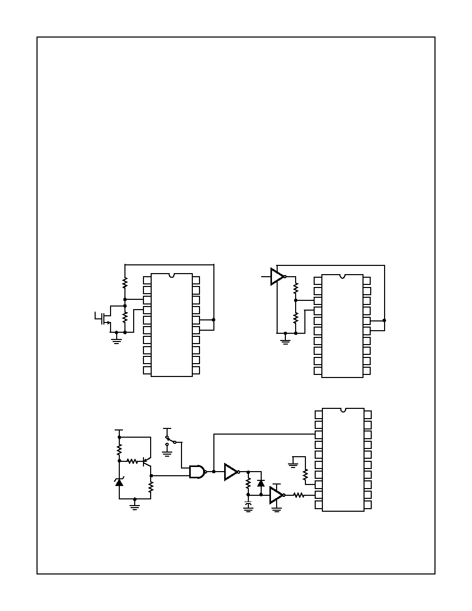
11
12
13
14
15
16
17
18
20
19
10
9
8
7
6
5
4
3
2
1 BHB
HEN
DIS
V
SS
OUT
IN+
HDEL
IN-
LDEL
AHB
BHO
BLO
BLS
V
DD
BHS
V
CC
ALS
ALO
AHS
AHO
100K
RDEL
RDEL
V
DD
0.1
µ
F
2N3906
V
DD
ENABLE
V
DD
56K
8.2V
56K
100K
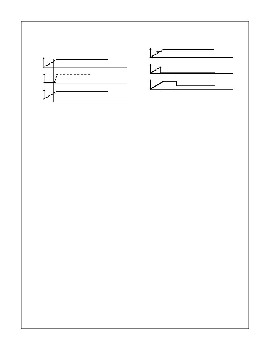
FIGURE 32.
V
DD
DIS
LDEL
=10ms
t1
t2
8.3V TO 9.1V (ASSUMING 5% ZENER TOLERANCE)
12V, FINAL VALUE
5.1V
NOTES:
2. Between t1 and t2 the IN+ and IN- inputs must cause the OUT pin to go through one complete cycle (transition order is not important). If
the ENABLE pin is low after the under-voltage circuit is satisfied, the ENABLE pin will initiate the 10ms time delay during which the IN+
and IN- pins must cycle at least once.
3. Another product, HIP4080A, incorporates undervoltage circuitry which eliminates the need for the above power up circuitry.
FIGURE 33. TIMING DIAGRAM FOR FIGURE 32
HIP4080
14
HIP4080
1
2
3
1
3
1
3
6
5
1
2
3
2
1
12
13
1
3
10
11
1
2
3
1
2
3
4
5
6
7
8
9
10
11
12
13
14
15
16
17
18
19
20
L1
R21
Q1
Q3
Q4
R22
L2
R23
C1
C3
JMPR1
R24
R30
R31
C2
R34
C4
CR2
CR1
Q2
JMPR5
JMPR3
JMPR2
JMPR4
R33
C5
C6
CX
CY
C8
U1
CW
CW
+
B+
IN2
IN1
BO
OUT/BLI
IN-/AHI
COM
IN+/ALI
+12V
+12V
BLS
AO
HEN/BHI
ALS
CD4069UB
CD4069UB
CD4069UB
CD4069UB
HIP4080/81
SECTION
CONTROL LOGIC
POWER SECTION
DRIVER SECTION
AHO
AHB
AHS
LDEL
ALO
HDEL
ALS
IN-/AHI
V
CC
IN+/ALI
V
DD
OUT/BLI
BLS
V
SS
BLO
DIS
BHS
HEN/BHI
BHO
BHB
R29
U2
U2
U2
U2
4
3
V
DD
CD4069UB
U2
8
9
CD4069UB
U2
V
DD
ENABLE
O
100K
0.1MFD
I
TO DIS
2N3906
56K
8.2V
56K
O
2
2
2
NOTES:
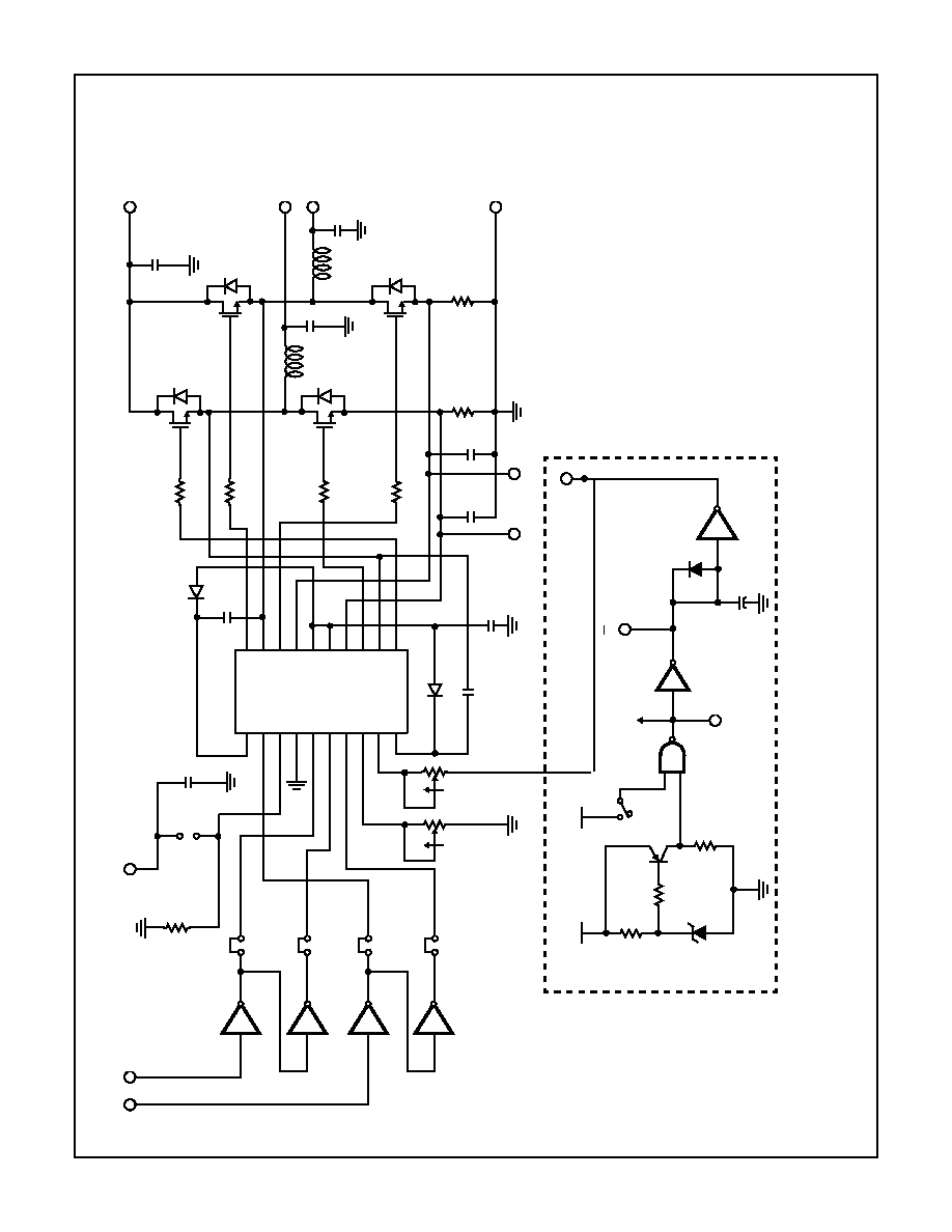
4. Circuit inside dashed area must be hardwired and
is not included on the evaluation board.
5. Device CD4069UB PIN 7 = COM, Pin 14 = +12V.
6. Components L1, L2, C1, C2, CX, CY, R30, R31,
are not supplied. refer to Application Note for de-
scription of input logic operation to determine
jumper locations for JMPR1 - JMPR4.
FIGURE 34. HIP4080 EVALUATION PC BOARD SCHEMATIC
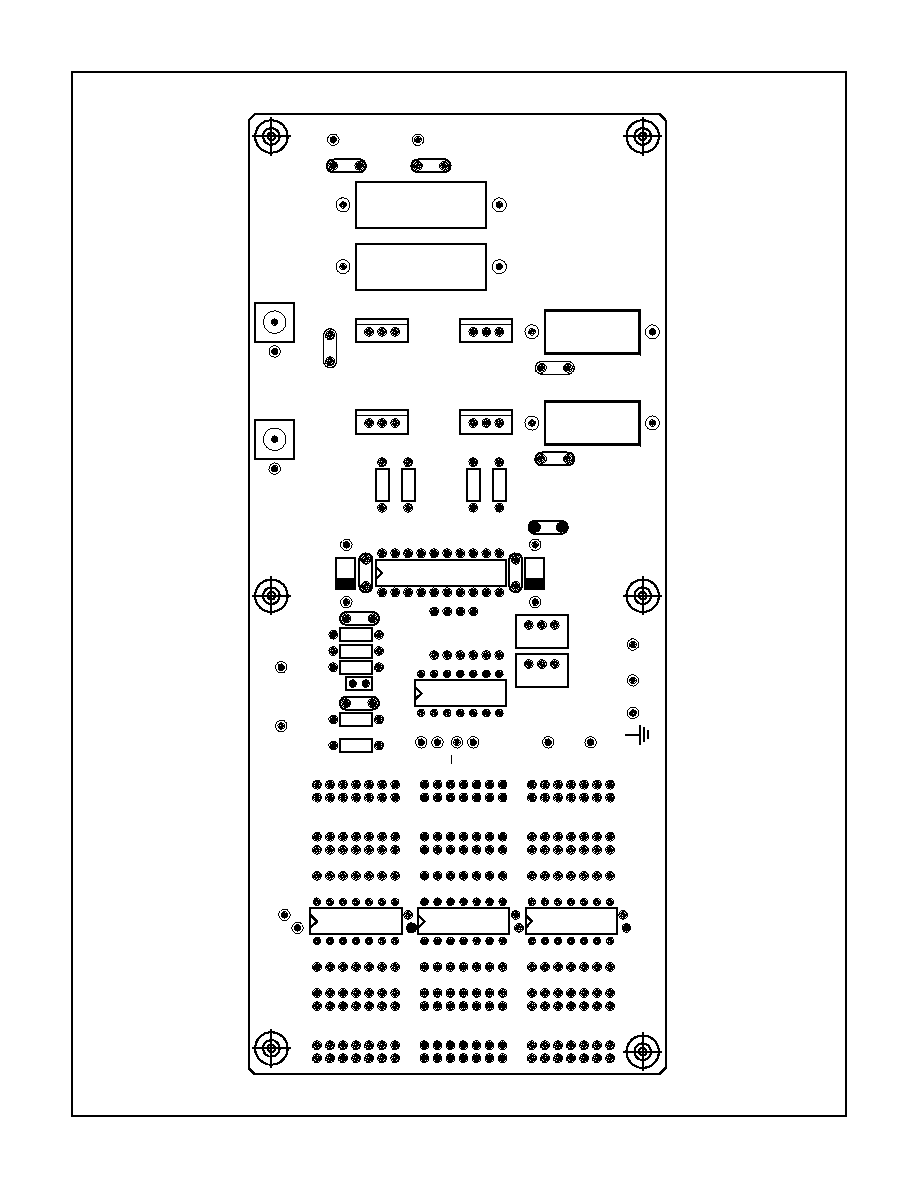
15
HIP4080
R22
1
Q3
L1
C1
JMPR2
JMPR5
R31
R33
CR2
R23
R24
R27
R28
R26
1
Q4
1
Q2
JMPR3
U1
R21
GND
L2
C3
C2
C4
JMPR4
JMPR1
R30
CR1
U2
R34
BO
AO
R32
I
O
C8
R29
C7
C6
C5
CY
CX
1
Q1
COM
+12V
B+
IN1
IN2
AHO
BHO
ALO
BLO
BLS
BLS
LDEL
HDEL
DIS
ALS
ALS
O
+
+
HIP4080/81
FIGURE 35. HIP4080 EVALUATION BOARD SILKSCREEN
16
Supplemental Information for HIP4080
and HIP4081 Power-Up Application
The HIP4080 and HIP4081 H-Bridge Driver ICs require
external circuitry to assure reliable start-up conditions of the
upper drivers. If not addressed in the application, the
H-bridge power MOSFETs may be exposed to shoot-
through current, possibly leading to MOSFET failure. Follow-
ing the instructions below will result in reliable start-up.
HIP4081
The HIP4081 has four inputs, one for each output. Outputs
ALO and BLO are directly controlled by input ALI and BLI.
By holding ALI and BLI low during start-up no shoot-through
conditions can occur. To set the latches to the upper drivers
such that the driver outputs, AHO and BHO, are off, the DIS
pin must be toggled from low to high after power is applied.
This is accomplished with a simple resistor divider, as shown
below in Figure 36. As the V
DD
/V
CC
supply ramps from zero
up, the DIS voltage is below its input threshold of 1.7V due to
the R1/R2 resistor divider. When V
DD
/V
CC
exceeds approxi-
mately 9V to 10V, DIS becomes greater than the input
threshold and the chip disables all outputs. It is critical that
ALI and BLI be held low prior to DIS reaching its threshold
level of 1.7V while V
DD
/V
CC
is ramping up, so that shoot
through is avoided. After power is up the chip can be
enabled by the ENABLE signal which pulls the DIS pin low.
HIP4080
The HIP4080 does not have an input protocol like the
HIP4081 that keeps both lower power MOSFETs off other
than through the DIS pin. IN+ and IN- are inputs to a com-
parator that control the bridge in such a way that only one of
the lower power devices is on at a time, assuming DIS is low.
However, keeping both lower MOSFETs off can be accom-
plished by controlling the lower turn-on delay pin, LDEL,
while the chip is enabled, as shown in Figure 37. Pulling
LDEL to V
DD
will indefinitely delay the lower turn-on delays
through the input comparator and will keep the lower MOS-
FETs off. With the lower MOSFETs off and the chip enabled,
i.e., DIS = low, IN+ or IN- can be switched through a full
cycle, properly setting the upper driver outputs. Once this is
accomplished, LDEL is released to its normal operating
point. It is critical that IN+/IN- switch a full cycle while LDEL
is held high, to avoid shoot-through. This start-up procedure
can be initiated by the supply voltage and/or the chip enable
command by the circuit in Figure 37.
FIGURE 36.
FIGURE 37.
11
12
13
14
15
16
17
18
20
19
10
9
8
7
6
5
4
3
2
1 BHB
BHI
DIS
V
SS
BLI
ALI
HDEL
AHI
LDEL
AHB
BHO
BLO
BLS
V
DD
BHS
V
CC
ALS
ALO
AHS
AHO
3.3K
R2
ENABLE
R1
15K
11
12
13
14
15
16
17
18
20
19
10
9
8
7
6
5
4
3
2
1 BHB
BHI
DIS
V
SS
BLI
ALI
HDEL
AHI
LDEL
AHB
BHO
BLO
BLS
V
DD
BHS
V
CC
ALS
ALO
AHS
AHO
3.3K
R2
R1
15K
ENABLE
11
12
13
14
15
16
17
18
20
19
10
9
8
7
6
5
4
3
2
1 BHB
HEN
DIS
V
SS
OUT
IN+
HDEL
IN-
LDEL
AHB
BHO
BLO
BLS
V
DD
BHS
V
CC
ALS
ALO
AHS
AHO
100K
RDEL
RDEL
V
DD
0.1
µ
F
2N3906
V
DD
ENABLE
V
DD
56K
8.2V
56K
100K
HIP4080
17
Timing Diagrams
NOTE:
7. ALI and/or BLI may be high after t1, whereupon the ENABLE pin
may also be brought high.
FIGURE 38.
NOTE:
8. Between t1 and t2 the IN+ and IN- inputs must cause the OUT pin
to go through one complete cycle (transition order is not impor-
tant). If the ENABLE pin is low after the undervoltage circuit is
satisfied, the ENABLE pin will initiate the 10ms time delay during
which the IN+ and IN- pins must cycle at least once.
FIGURE 39.
V
DD
DIS
ALI, BLI
8.5V TO 10.5V (ASSUMES 5% RESISTORS)
1.7V
12V, FINAL VALUE
V
DD
DIS
LDEL
=10ms
t1
t2
8.3V TO 9.1V (ASSUMING 5% ZENER TOLERANCE)
12V, FINAL VALUE
5.1V
HIP4080
18
HIP4080
NOTES:
1. Symbols are defined in the "MO Series Symbol List" in Section
2.2 of Publication Number 95.
2. Dimensioning and tolerancing per ANSI Y14.5M-1982.
3. Dimension "D" does not include mold flash, protrusions or gate
burrs. Mold flash, protrusion and gate burrs shall not exceed
0.15mm (0.006 inch) per side.
4. Dimension "E" does not include interlead flash or protrusions. In-
terlead flash and protrusions shall not exceed 0.25mm (0.010
inch) per side.
5. The chamfer on the body is optional. If it is not present, a visual
index feature must be located within the crosshatched area.
6. "L" is the length of terminal for soldering to a substrate.
7. "N" is the number of terminal positions.
8. Terminal numbers are shown for reference only.
9. The lead width "B", as measured 0.36mm (0.014 inch) or greater
above the seating plane, shall not exceed a maximum value of
0.61mm (0.024 inch)
10. Controlling dimension: MILLIMETER. Converted inch dimen-
sions are not necessarily exact.
INDEX
AREA
E
D
N
1
2
3
-B-
0.25(0.010)
C A
M
B S
e
-A-
L
B
M
-C-
A1
A
SEATING PLANE
0.10(0.004)
h x 45
o
C
H
0.25(0.010)
B
M
M
M20.3
(JEDEC MS-013-AC ISSUE C)
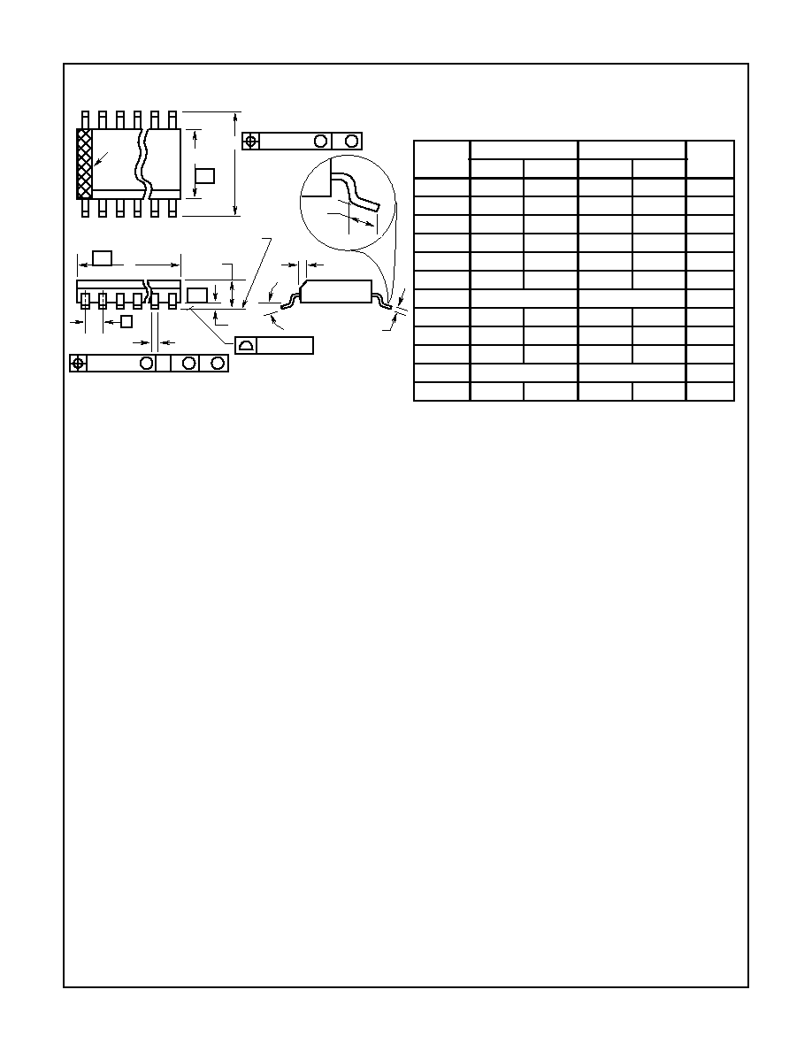
20 LEAD WIDE BODY SMALL OUTLINE PLASTIC PACKAGE
SYMBOL
INCHES
MILLIMETERS
NOTES
MIN
MAX
MIN
MAX
A
0.0926
0.1043
2.35
2.65
-
A1
0.0040
0.0118
0.10
0.30
-
B
0.013
0.0200
0.33
0.51
9
C
0.0091
0.0125
0.23
0.32
-
D
0.4961
0.5118
12.60
13.00
3
E
0.2914
0.2992
7.40
7.60
4
e
0.050 BSC
1.27 BSC
-
H
0.394
0.419
10.00
10.65
-
h
0.010
0.029
0.25
0.75
5
L
0.016
0.050
0.40
1.27
6
N
20
20
7
0
o
8
o
0
o
8
o
-
Rev. 0 12/93
Small Outline Plastic Packages (SOIC)
19
HIP4080
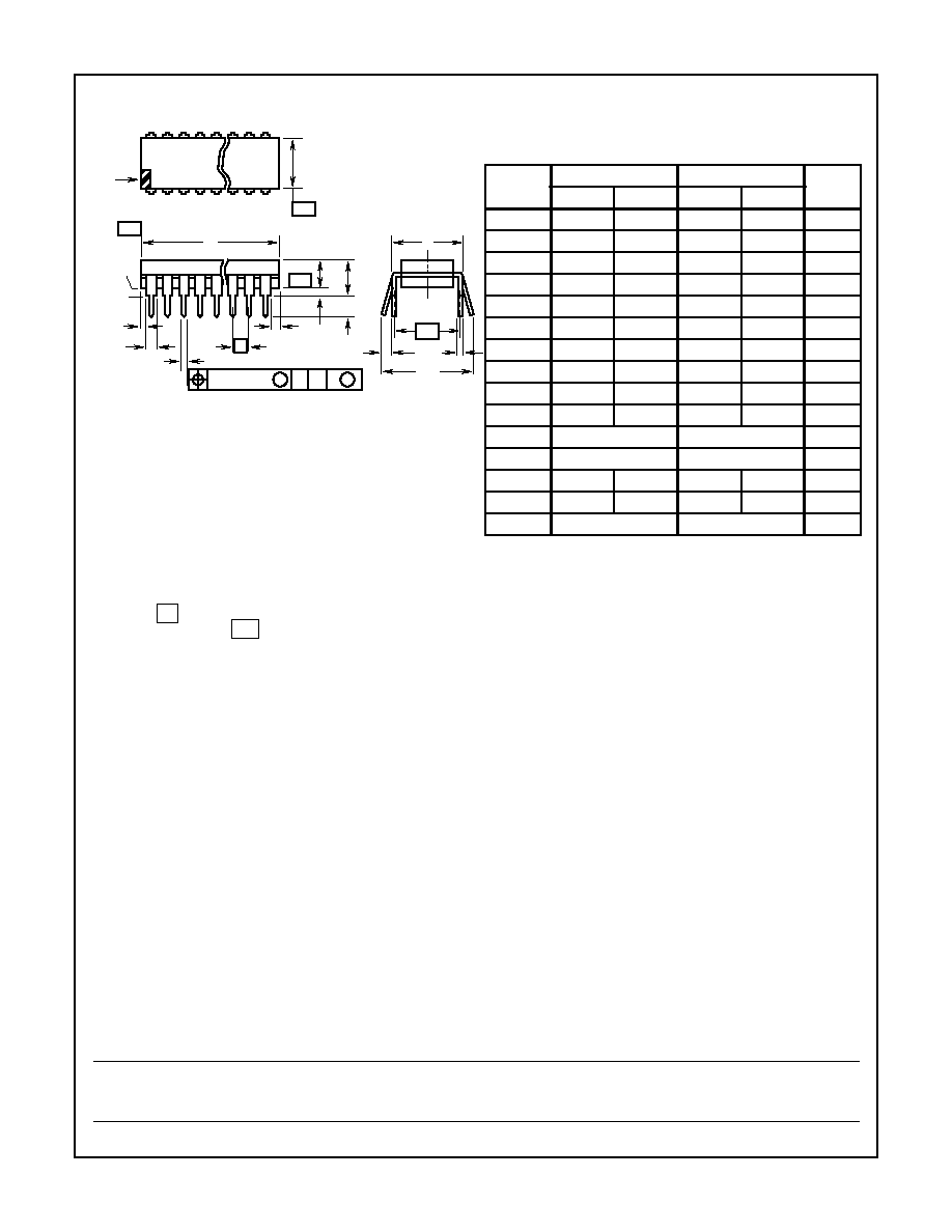
E20.3
(JEDEC MS-001-AD ISSUE D)
20 LEAD DUAL-IN-LINE PLASTIC PACKAGE
SYMBOL
INCHES
MILLIMETERS
NOTES
MIN
MAX
MIN
MAX
A
-
0.210
-
5.33
4
A1
0.015
-
0.39
-
4
A2
0.115
0.195
2.93
4.95
-
B
0.014
0.022
0.356
0.558
-
B1
0.045
0.070
1.55
1.77
8
C
0.008
0.014
0.204
0.355
-
D
0.980
1.060
24.89
26.9
5
D1
0.005
-
0.13
-
5
E
0.300
0.325
7.62
8.25
6
E1
0.240
0.280
6.10
7.11
5
e
0.100 BSC
2.54 BSC
-
e
A
0.300 BSC
7.62 BSC
6
e
B
-
0.430
-
10.92
7
L
0.115
0.150
2.93
3.81
4
N
20
20
9
Rev. 0 12/93
NOTES:
1. Controlling Dimensions: INCH. In case of conflict between
English and Metric dimensions, the inch dimensions control.
2. Dimensioning and tolerancing per ANSI Y14.5M-1982.
3. Symbols are defined in the "MO Series Symbol List" in Section
2.2 of Publication No. 95.
4. Dimensions A, A1 and L are measured with the package seated
in JEDEC seating plane gauge GS-3.
5. D, D1, and E1 dimensions do not include mold flash or protru-
sions. Mold flash or protrusions shall not exceed 0.010 inch
(0.25mm).
6. E and
are measured with the leads constrained to be per-
pendicular to datum
.
7. e
B
and e
C
are measured at the lead tips with the leads uncon-
strained. e
C
must be zero or greater.
8. B1 maximum dimensions do not include dambar protrusions.
Dambar protrusions shall not exceed 0.010 inch (0.25mm).
9. N is the maximum number of terminal positions.
10. Corner leads (1, N, N/2 and N/2 + 1) for E8.3, E16.3, E18.3,
E28.3, E42.6 will have a B1 dimension of 0.030 - 0.045 inch
(0.76 - 1.14mm).
C
L
E
e
A
C
e
B
e
C
-B-
E1
INDEX
1 2 3
N/2
N
AREA
SEATING
BASE
PLANE
PLANE
-C-
D1
B1
B
e
D
D1
A
A2
L
A1
-A-
0.010 (0.25)
C
A
M
B S
e
A
-C-
Dual-In-Line Plastic Packages (PDIP)
All Intersil semiconductor products are manufactured, assembled and tested under ISO9000 quality systems certification.
Intersil products are sold by description only. Intersil Corporation reserves the right to make changes in circuit design and/or specifications at any time without
notice. Accordingly, the reader is cautioned to verify that data sheets are current before placing orders. Information furnished by Intersil is believed to be accurate
and reliable. However, no responsibility is assumed by Intersil or its subsidiaries for its use; nor for any infringements of patents or other rights of third parties which
may result from its use. No license is granted by implication or otherwise under any patent or patent rights of Intersil or its subsidiaries.
For information regarding Intersil Corporation and its products, see web site http://www.intersil.com