 | –≠–ª–µ–∫—Ç—Ä–æ–Ω–Ω—ã–π –∫–æ–º–ø–æ–Ω–µ–Ω—Ç: HIP9010 | –°–∫–∞—á–∞—Ç—å:  PDF PDF  ZIP ZIP |
4-1
HIP9010
Engine Knock Signal Processor
The HIP9010 is used to provide a method of detecting
premature detonation or "Knock" in automotive engines.
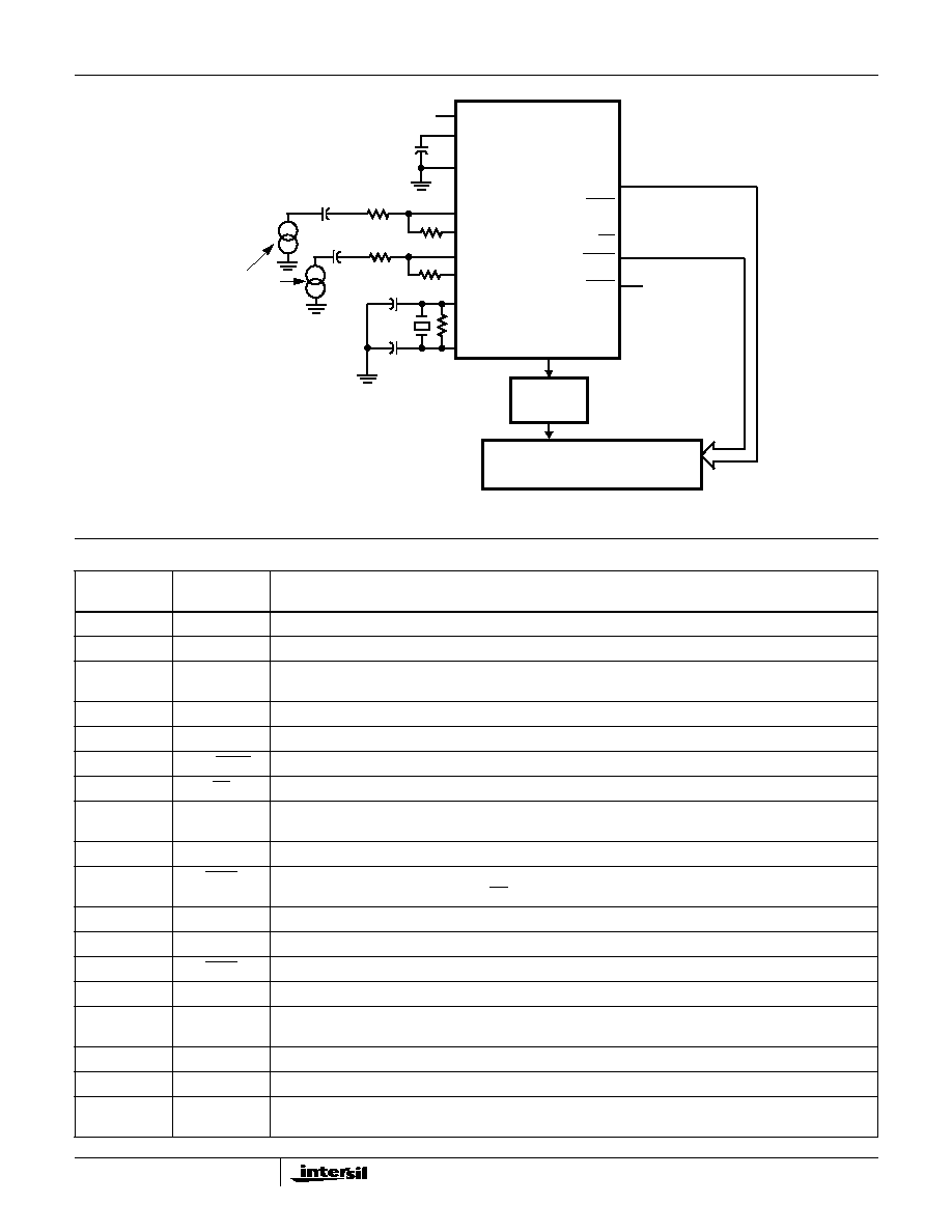
A block diagram of this IC is shown in Figure 1. The chip
alternately selects one of the two sensors mounted on the
engine block. Two programmable bandpass filters process
the signal from both sensors, and divides the signal into two
channels. When the engine is not knocking, programmable
gain adjust stages are set to ensure that both the reference
channel and the knock channel contain similar energies.
This technique ensures that the detection system is
comparatively immune to changes in the engine background
noise level. When the engine is knocking, the energy in the
knock channel increases.
Features
∑ Two Sensor Inputs
∑ Microprocessor Programmable
∑ Accurate and Stable Filter Elements
∑ Digitally Programmable Gain
∑ Digitally Programmable Time Constants
∑ Digitally Programmable Filter Characteristics
∑ On-Chip Clock
∑ Operating Temperature Range -40
o
C to 125
o
C
Applications
∑ Engine Knock Detector Processor
∑ Analog Signal Processing where Controllable Filter
Characteristics are Required
Pinout
HIP9010
(SOIC)
TOP VIEW
Ordering Information
PART NUMBER
TEMP.
RANGE (
o
C)
PACKAGE
PKG.
NO.
HIP9010AB
-40 to 125
20 Ld SOIC (W)
M20.3
11
12
13
14
15
16
17
18
20
19
10
9
8
7
6
5
4
3
2
1
V
DD
GND
V
MID
INOUT
NC
NC
CS
INT/HOLD
OSCIN
OSCOUT
S0IN
S1FB
S1IN
NC
S0FB
NC
TEST
SCK
MOSI
MISO
Data Sheet
November 1998
File Number
3601.4
CAUTION: These devices are sensitive to electrostatic discharge; follow proper IC Handling Procedures.
http://www.intersil.com or 407-727-9207
|
Copyright
©
Intersil Corporation 1999

4-2
HIP9010
Simplified Block Diagram
ANTIALIASING
FIL
TER
3RD ORDER
-
+
-
+
KNOCK FREQUENCY CHANNEL
REFERENCE FREQUENCY CHANNEL
TO SWITCHED
CAPACITOR
NETWORKS
(14) TEST
PROGRAMMABLE
BANDPASS
FILTER
1-20kHz
64 STEPS
PROGRAMMABLE
GAIN
STAGE
1-0.133
64 STEPS
PROGRAMMABLE
BANDPASS
FILTER
1-20kHz
64 STEPS
PROGRAMMABLE
GAIN
STAGE
1-0.133
64 STEPS
ACTIVE
FULL WAVE
RECTIFIER
REGISTERS
AND
STATE MACHINE
SPI
INTERSPACE
POWER SUPPLY
AND
BIAS CIRCUITS
(17) S1IN
(18) S1FB
(20) S0IN
(19) S0FB
(2) GND
OSCIN (9)
OSCOUT (10)
SCK (13)
CS (8)
MOSI (12)
MISO (11)
INT/HOLD (7)
DIFFERENTIAL
TO
SINGLE-ENDED
CONVERTER
AND OUTPUT
DRIVER
PROGRAMMABLE
INTEGRATOR
40-600
µ
s
32 STEPS
ACTIVE
FULL WAVE
RECTIFIER
INOUT (4)
(1) V
DD
(3) V
MID
CLOCK
CHANNEL SELECT
SWITCHES
FIGURE 1.

4-3
Absolute Maximum Ratings
Thermal Information
DC Logic Supply, V
DD
. . . . . . . . . . . . . . . . . . . . . . . . -0.5V to +7.0V
Output Voltage, V
O
. . . . . . . . . . . . . . . . . . . . . . . . . . -0.5V to +7.0V
Input Voltage, V
IN
. . . . . . . . . . . . . . . . . . . . . . . . . . . . . . +7V (Max)
Operating Conditions
Temperature Range . . . . . . . . . . . . . . . . . . . . . . . . . -40
o
C to 125
o
C
Thermal Resistance (Typical, Note 1)
JA
(
o
C/W)
SOIC Package . . . . . . . . . . . . . . . . . . . . . . . . . . . . .
115
Maximum Storage Temperature Range, T
STG
. . . . -65
o
C to 150
o
C
Maximum Junction Temperature . . . . . . . . . . . . . . . . . . . . . . .150
o
C
Maximum Lead Temperature (Soldering) . . . . . . . . . . . . . . . 300
o
C
At distance 1/16in
±
1/32in (1.59mm
±
0.79mm) from case
for 10s (Max)
(SOIC - Lead Tips Only)
CAUTION: Stresses above those listed in "Absolute Maximum Ratings" may cause permanent damage to the device. This is a stress only rating and operation of the
device at these or any other conditions above those indicated in the operational sections of this specification is not implied.
NOTE:
1.
JA
is measured with the component mounted on an evaluation PC board in free air.
Electrical Specifications
V
DD
= 5V,
±
5%, GND = 0V, Clock Frequency 4MHz,
±
0.5%, T
A
= -40
o
C to 125
o
C,
Unless Otherwise Specified
PARAMETER
SYMBOL
TEST CONDITIONS
MIN
TYP
MAX
UNITS
DC ELECTRICAL CHARACTERISTICS
Quiescent Supply Current
I
DD
V
DD
= 5.25V, GND = 0V
3
7.5
12
mA
Midpoint Voltage, Pin 3
V
MID
V
DD
= 5.0V, I
L
= 2mA Source
2.3
2.45
2.55
V
Midpoint Voltage, Pin 3
V
MID
V
DD
= 5.0V, I
L
= 0mA
2.4
2.5
2.6
V
Input Leakage, Pin 14
IL
TEST
Measured at V
DD
= 5.0V
-
-
3
µ
A
Internal Pull-Up Resistance, Pin 14
R
TEST
V
DD
= 5.0V, I Measure = 15
µ
A
30
100
200
K
Leakage of Pins 7, 8, 12 and 13
I
L
Measured at GND and V
DD
= 5V
-
-
±
3
µ
A
Low Input Voltage, Pins 7, 8, 12 and 13
V
IL
-
-
30
% of V
DD
High Input Voltage, Pins 7, 8, 12 and 13
V
IH
70
-
-
% of V
DD
Low Level Output, Pin 11
V
OL
I
SOURCE
= 4mA
0.01
-
0.30
V
Leakage Pin 11
I
L
Measured at GND and V
DD
= 5V
-
-
±
10
µ
A
Low Level Output, Pin 10
V
OL
I
SOURCE
= 500
µ
A, V
DD
= 5V
-
-
1.5
V
High Level Output, Pin 10
V
OH
I
SINK
= -500
µ
A, V
DD
= 5V
4.4
-
-
V
INPUT AMPLIFIERS
S0FB and S1FB High Output Voltage
V
OUT
HI
100
µ
A I
SINK
, V
DD
= 5V
4.7
4.9
-
V
S0FB and S1FB Low Output Voltage
V
OUT
LO
100
µ
A I
SOURCE
, V
DD
= 5V
-
15
200
mV
S0FB and S1FB Closed Loop
A
CL
Input Resistor = 1M
,
Feedback Resistor = 49.9k
-25
-26
-27
dB
S0FB and S1FB Closed Loop
A
CL
Input Resistor = 47.5k
,
Feedback Resistor = 475k
18
20
21
dB
ANTIALIASING FILTER
Response 1kHz to 20kHz,
Referenced to 1kHz
BW
Test Mode, 70mV
RMS
Input to S0FB or
S1FB, Output Pin 4
-
-2
-
dB
Attenuation at 180kHz
Referenced to 1kHz
ATEN
Test Mode, 70mV
RMS
Input to S0FB or
S1FB, Output Pin 4
-10
-15
-
dB
PROGRAMMABLE FILTERS
Peak to Peak Voltage Output
V
OUTP-P
Run Mode
3.5
4.0
-
V
P-P
Filters Q (Note 2)
Q
Run Mode
-
2.5
-
Q
PROGRAMMABLE GAIN AMPLIFIERS
Percent Amplifier Gain Deviation
Per Table 2
%G
Run Mode
-
±
1
-
%
HIP9010

4-4
INTEGRATOR
Integrator Offset Voltage
INTGV
IO
By Design
-
0.1
-
mV
Integrator Reset Voltage
V
RESET
Pin 4 Voltage at Initiation of
Integration Cycle. V
DD
= 5V
430
500
570
mV
Integrator Droop after 500
µ
s
V
DROOP
Hold Mode, Pin 7 = 0V, V
DD
= 5V,
Pin 4 set to 20% to 80% of V
DD
-
±
3
±
50
mV
OUTPUT AND SAMPLE AND HOLD
Differential to Single Ended
Converter Offset Voltage
DIFV
IO
By Design
-
0.1
-
mV
Change in Converter Output
DIFOUT
Run Mode, 500
µ
A, Sinking to No Load
-
±
1
±
3
mV
SYSTEM GAIN DEVIATION
Gain Deviation from "Ideal Equation"
Correlation, Factor - 5.0%
V
OUT
-
V
RESET
Run Mode, maximum signal output
from Input Amplifier <2.25V
P-P
,
Equation Output x 0.95 + Device
Reset Voltage. For Total V
OUT
4.7V
-8%,
±
100mV
Equation
x 0.95
-V
RESET
8%,
±
100mV
V
NOTE:
2. Q = f
O
/BW, Where: f
O
= Center Frequency, BW = 3dB bandwidth.
Ideal Equation
When the two filters are set to the same frequency and the input signal is present for the periods T
IN
, then:
G
R
and G
K
= Programed Gain of Reference and Knock channels.
T
IN
= Time input signal is present In ms.
T
C
= Programmed integrator time constant ms.
N = Number of cycles of input signal.
f
Q
= Frequency of input signal. Assumes both filters are programmed to the same frequency.
V
RESET
= Integrator Reset Voltage.
1.273 = 4/
R
F
= Feedback resistor value.
R
IN
= Signal input resistor value.
For example, assume 300mV
P-P
input with the time constant programmed to 300
µ
s and the Integration time is 1.2ms. The R
F
/R
IN
ratio is one and
the Reference channel is programmed to a Gain of 0.188. The Knock channel is then automatically set to a gain of one. The input signal is contin-
uous for the total integration time, T
IN
.
Electrical Specifications
V
DD
= 5V,
±
5%, GND = 0V, Clock Frequency 4MHz,
±
0.5%, T
A
= -40
o
C to 125
o
C,
Unless Otherwise Specified (Continued)
PARAMETER
SYMBOL
TEST CONDITIONS
MIN
TYP
MAX
UNITS
INTOUT volts
(
)
Input signal (V
P
P
≠
)
R
F
R
IN
----------
◊
G
K
1.273
N
TC (ms)
f
Q
(kHz)
◊
---------------------------------------------------
◊
◊
G
R
1.273
N
TC (ms)
f
Q
(kHz)
◊
---------------------------------------------------
◊
◊
≠
V
RESET
+
=
INTOUT volts
(
)
Input signal (V
P
P
≠
)
R
F
R
IN
----------
◊
1.273
T
IN
TC
---------
G
K
G
R
≠
(
)
◊
V
RESET
+
=
INTOUT volts
(
)
0.3V (V
P
P
≠
)
1.273
1.2ms
0.300ms
-----------------------
1.000
0.188
≠
(
)
◊
◊
◊
V
RESET
1.24V
0.500V
1.74V
=
+
=
+
=
HIP9010
4-5
+5V
HIP9010
MICROPROCESSOR
SPI BUS
C3, 0.022
µ
F
C2, 3.3nF
C1, 3.3nF
R1
R4
R3
4MHz
A/D
CONVERTER
V
DD
V
MID
GND
S1IN
S1FB
S0IN
S0FB
OSCIN
OSCOUT
INTOUT
MOSI
MISO
SCK
CS
INT/HOLD
TEST
TRANSDUCERS
R2
FIGURE 2. SIMPLIFIED BLOCK DIAGRAM OF THE HIP9010 IN AN AUTOMOTIVE APPLICATION
20pF
20pF
1M
Pin Descriptions
PIN
NUMBER
SYMBOL
DESCRIPTION
1
V
DD
5V power input.
2
GND
This terminal is tied to ground.
3
V
MID
This terminal is tied to the internal mid-supply generator and is brought out for supply bypassing by a 0.022
µ
F
capacitor.
4
INTOUT
Buffered output of the integrator.
5 and 6
NC
These terminals are not internally connected. DO NOT USE.
7
INT/HOLD
Selects whether the chip is in the Integrate Mode (Input High) or in the Hold Mode (Input Low).
8
CS
A low input on this pin enables the chip to communicate over the SPI bus.
9
OSCIN
Input to inverter used for the oscillator circuit. A 4MHz crystal or ceramic resonator is connected between this
pin and pin 10. To bias the inverter, a 1.0M
to 10M
resistor is usually connected between this pin and pin 10.
10
OSCOUT
Output of the inverter used for the oscillator. See pin 9 above.
11
MISO
Output of the chip SPI data bus. It is the inversion of the chip DATAIN line. This is an open drain output. The
output must be disabled by placing the CS High when the chip is not selected.
12
MOSI
Input of the chip SPI data bus. Data length is eight bits.
13
SCK
Input from the SPI clock. Normally high, the data is clocked to the chip internal circuitry on the rising clock edge.
14
TEST
A low on this pin places the chip in the test mode. For normal operation this terminal is tied high or left open.
15 and 16
NC
These terminals are not internally connected. DO NOT USE.
17
S1IN
Inverting input to sensor one amplifier. A resistor is tied from this summing input to the transducer. A second
resistor is tied between this terminal and terminal 18, S1FB to establish the gain of the amplifier.
18
S1FB
Output of the sensor one amplifier. This terminal is used to apply feedback.
19
S0FB
Output of the sensor zero amplifier. This terminal is used to apply feedback.
20
S0IN
Inverting input to sensor zero amplifier. A resistor is tied from this summing input to the transducer. A second
resistor is tied between this terminal and terminal 19, S0FB to establish the gain of the amplifier.
HIP9010