
TM
1
FN6021.1
ISL5929
Dual 14-Bit, +3.3V, 130/210+MSPS,
CommLink
TM
High Speed D/A Converter
The ISL5929 is a dual 14-bit,
130/210+MSPS (Mega Samples
Per Second), CMOS, high speed,
low power, D/A (digital to analog) converter, designed
specifically for use in high performance communication
systems such as base transceiver stations utilizing 2.5G or
3G cellular protocols.
This device complements the CommLink ISL5x61 and
ISL5x29 families of high speed converters, which include 8-,
10-, 12-, and 14-bit devices.
Pinout
ISL5929
(LQFP)
TOP VIEW
Features
� Speed Grades . . . . . . . . . . . . . . . . 130M and 210+MSPS
� Low Power . . . . . 233mW with 20mA Output at 130MSPS
� Adjustable Full Scale Output Current . . . . . 2mA to 20mA
� Guaranteed Gain Matching < 0.14dB
� +3.3V Power Supply
� 3V LVCMOS Compatible Inputs
� Excellent Spurious Free Dynamic Range
(75dBc to Nyquist, f
S
= 130MSPS, f
OUT
= 10MHz)
� UMTS Adjacent Channel Power = 71dB at 19.2MHz
� EDGE/GSM SFDR = 94dBc at 11MHz in 20MHz Window
� Dual, 3.3V, Lower Power Replacement for AD9767
Applications
� Cellular Infrastructure - Single or Multi-Carrier: IS-136,
IS-95, GSM, EDGE, CDMA2000, WCDMA, TDS-CDMA
� BWA Infrastructure
� Quadrature Transmit with IF Range 0�80MHz
� Medical/Test Instrumentation and Equipment
� Wireless Communication Systems
Ordering Information
PART
NUMBER
TEMP.
RANGE
(
o
C)
PACKAGE
PKG. NO.
CLOCK
SPEED
ISL5929IN
-40 to 85
48 Ld LQFP
Q48.7x7A 130MHz
ISL5929/2IN
-40 to 85
48 Ld LQFP
Q48.7x7A 210MHz
ISL5929EVAL1
25
Evaluation Platform
210MHz
1
2
3
4
5
6
7
8
32
31
30
29
28
27
26
25
24
23
22
21
20
19
18
17
9
10
11
12
13 14 15 16
33
34
35
36
37
38
39
40
41
42
43
44
45
46
47
48
QD6
QD7
QD8
QD9
QD10
QD11
QD12
QD13 (MSB)
CLK
DGND
AGND
QCOMP
ID7
ID6
ID5
ID4
ID3
(LSB) ID0
SLEEP
D
VDD
AGND
ICOMP
ID2
ID1
ID8
ID9
ID10
ID11
ID12
QD0 (LSB)
QD1
QD2
QD3
QD4
QD5
ID13(MSB)
A
VDD
NC
IOUT
A
IOUTB
REFIO
REFLO
AG
N
D
FSADJ
QOUTB
QOUT
A
NC
A
VDD
Data Sheet
February 2002
CAUTION: These devices are sensitive to electrostatic discharge; follow proper IC Handling Procedures.
1-888-INTERSIL or 321-724-7143
|
Intersil (and design) is a trademark of Intersil Americas Inc.
Copyright � Intersil Americas Inc. 2002. All Rights Reserved
CommLinkTM is a trademark of Intersil Americas Inc.

2
Typical Applications Circuit
+3.3V POWER SOURCE
1�F
50
1.91k
FERRITE
10�H
BEAD
R
SET
1
2
3
4
5
6
7
8
32
31
30
29
28
27
26
25
24
23
22
21
20
19
18
17
9
10
11
12
13 14 15 16
33
34
35
36
37
38
39
40
41
42
43
44
45
46
47
48
AV
PP
ID7
QD0 (LSB)
ID6
ID5
ID4
ID1
ID0 (LSB)
QD1
QD2
QD8
QD9
QD10
QD11
QD12
QD13 (MSB)
SLEEP
D
VDD
AGND
A
GND
AGND
DGND
QD3
ID10
ID11
ID12
ID13 (MSB)
FSADJ
REFIO
REFLO
0.1�F
0.1�F
ICOMP
AV
PP
0.1�F
AV
PP
A
VDD
A
VDD
0.1�F
DV
PP
0.1�F
QCOMP
CLK
+
10�F
1�F
FERRITE
10�H
BEAD
DV
PP
+
10�F
0.1�F
0.1�F
0.1�F
C
1
C
2
C
4
C
3
R
1
C
5
C
6
C
9
C
10
L
1
C
12
C
13
C
11
C
14
L
2
(DIGITAL POWER PLANE) = +3.3V
(ANALOG POWER PLANE) = +3.3V
ID8
ID9
QD6
QD7
QD4
QD5
ID3
ID2
ANY 50 LOAD
REPRESENTS
(50)
(50)
50
50
QOUT
IOUT
1:1 TRANSFORMER
R
2
R
3
ISL5929

3
Functional Block Diagram
UPPER
(LSB) QD0
QD1
QD2
QD3
QD4
QD5
QD6
QD9
CLK
QD7
QD8
5-BIT
DECODER
CASCODE
CURRENT
SOURCE
SWITCH
MATRIX
40
40
31 MSB
SEGMENTS
9 LSBs
+
QD10
QD11
QD12
(MSB) QD13
INPUT
LATCH
UPPER
(LSB) ID0
ID1
ID2
ID3
ID4
ID5
ID6
ID9
ID7
ID8
5-BIT
DECODER
REFIO
CASCODE
CURRENT
SOURCE
SWITCH
MATRIX
40
40
31 MSB
SEGMENTS
9 LSBs
+
ID10
ID11
ID12
(MSB) ID13
INPUT
LATCH
REFLO
FSADJ
SLEEP
QOUTA
QOUTB
IOUTA
IOUTB
QCOMP
ICOMP
VOLTAGE
REFERENCE
BIAS
GENERATION
INT/EXT
ISL5929

4
Pin Descriptions
PIN NO.
PIN NAME
PIN DESCRIPTION
11, 19, 26
AGND
Analog ground.
13, 24
A
VDD
Analog supply (+2.7V to +3.6V).
28
CLK
Clock Iinput.
27
DGND
Connect to digital ground.
10
D
VDD
Digital supply (+2.7V to +3.6V).
20
FSADJ
Full scale current adjust. Use a resistor to ground to adjust full scale output current. Full scale output
current = 32 x V
FSADJ
/R
SET
.
14, 23
NC
Not internally connected. Recommend no connect.
12, 25
ICOMP, QCOMP
Compensation pin for internal bias generation. Each pin should be individually decoupled to AGND with
a 0.1
�
F capacitor.
1-8, 29-48
ID13-ID0, QD13-QD0 Digital data input ports. Bit 13 is most significant bit (MSB) and bit 0 is the least significant bit (LSB).
15, 22
IOUTA, QOUTA
Current outputs of the device. Full scale output current is achieved when all input bits are set to binary 1.
16, 21
IOUTB, QOUTB
Complementary current outputs of the device. Full scale output current is achieved on the complementary
outputs when all input bits are set to binary 0.
17
REFIO
Reference voltage input if Internal reference is disabled. The internal reference is not intended to drive an
external load. Use 0.1
�
F cap to ground when internal reference is enabled.
18
REFLO
Connect to analog ground to enable internal 1.2V reference or connect to AV
DD
to disable internal reference.
9
SLEEP
Connect to digital ground or leave floating for normal operation. Connect to DV
DD
for sleep mode.
ISL5929
5
Absolute Maximum Ratings
Thermal Information
Digital Supply Voltage DV
DD
to DGND . . . . . . . . . . . . . . . . . . +3.6V
Analog Supply Voltage AV
DD
to AGND . . . . . . . . . . . . . . . . . . +3.6V
Grounds, AGND TO DGND . . . . . . . . . . . . . . . . . . . . -0.3V to +0.3V
Digital Input Voltages (DATA, CLK, SLEEP). . . . . . . . . DV
DD
+ 0.3V
Reference Input Voltage Range . . . . . . . . . . . . . . . . . . AV
DD
+ 0.3V
Analog Output Current (I
OUT
) . . . . . . . . . . . . . . . . . . . . . . . . . 24mA
Operating Conditions
Temperature Range . . . . . . . . . . . . . . . . . . . . . . . . . . .-40�C to 85�C
Thermal Resistance (Typical, Note 1)
JA
(�C/W)
LQFP Package . . . . . . . . . . . . . . . . . . . . . . . . . . . . .
70
Maximum Junction Temperature . . . . . . . . . . . . . . . . . . . . . . . 150�C
Maximum Storage Temperature Range . . . . . . . . . . . -65�C to 150�C
Maximum Lead Temperature (Soldering 10s) . . . . . . . . . . . . . 300�C
CAUTION: Stresses above those listed in "Absolute Maximum Ratings" may cause permanent damage to the device. This is a stress only rating and operation of the
device at these or any other conditions above those indicated in the operational sections of this specification is not implied.
NOTE:
1.
JA
is measured with the component mounted on an evaluation PC board in free air.
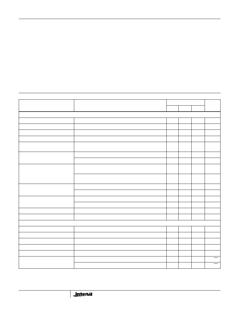
Electrical Specifications
AV
DD
= DV
DD
= +3.3V, V
REF
= Internal 1.2V, IOUTFS = 20mA, T
A
= 25�C for All Typical Values
PARAMETER
TEST CONDITIONS
T
A
= -40�C TO 85�C
UNITS
MIN
TYP
MAX
SYSTEM PERFORMANCE
Resolution
14
-
-
Bits
Integral Linearity Error, INL
"Best Fit" Straight Line (Note 7)
-5
�
2.5
+5
LSB
Differential Linearity Error, DNL
(Note 7)
-3
�
1.5
+3
LSB
Offset Error, I
OS
IOUTA (Note 7)
-0.006
+0.006
% FSR
Offset Drift Coefficient
(Note 7)
-
0.1
-
ppm
FSR/�C
Full Scale Gain Error, FSE
With External Reference (Notes 2, 7)
-3
�
0.5
+3
% FSR
With Internal Reference (Notes 2, 7)
-3
�
0.5
+3
% FSR
Full Scale Gain Drift
With External Reference (Note 7)
-
�
50
-
ppm
FSR/�C
With Internal Reference (Note 7)
-
�
100
-
ppm
FSR/�C
Crosstalk
f
CLK
= 100MSPS, f
OUT
= 10MHz
-
83
-
dB
f
CLK
= 100MSPS, f
OUT
= 40MHz
-
74
-
dB
Gain Matching Between Channels
(DC Measurement)
As a percentage of Full Scale Range
-1.6
0.6
+1.6
% FSR
In dB Full Scale Range
-0.14
0.05
+0.14
dB FSR
Full Scale Output Current, I
FS
2
20
22
mA
Output Voltage Compliance Range
(Note 3)
-1.0
-
1.25
V
DYNAMIC CHARACTERISTICS
Maximum Clock Rate, f
CLK
ISL5929/2IN
210
250
-
MHz
Maximum Clock Rate, f
CLK
ISL5929IN
130
150
-
MHz
Output Rise Time
Full Scale Step
-
1
-
ns
Output Fall Time
Full Scale Step
-
1
-
ns
Output Capacitance
-
5
-
pF
Output Noise
IOUTFS = 20mA
-
50
-
pA/
Hz
IOUTFS = 2mA
-
30
-
pA/
Hz
ISL5929