 | –≠–Ľ–Ķ–ļ—ā—Ä–ĺ–Ĺ–Ĺ—č–Ļ –ļ–ĺ–ľ–Ņ–ĺ–Ĺ–Ķ–Ĺ—ā: ISL6292D | –°–ļ–į—á–į—ā—Ć:  PDF PDF  ZIP ZIP |

1
ģ
FN9166
ISL6292D
Li-ion/Li Polymer Battery Charger
The ISL6292D is an integrated single-cell Li-ion or
Li-polymer battery charger capable of operating with an input
voltage as low as 2.4V. This charger is designed to work with
various types of ac adapters or a USB port.
The ISL6292D operates as a linear charger when the ac
adapter is a voltage source. The battery is charged in a
CC/CV (constant current/constant voltage) profile. The
charge current is programmable up to 2A. The ISL6292D
can also work with a current-limited adapter to minimize the
thermal dissipation, in which case the ISL6292D combines
the benefits of both a linear charger and a pulse charger.
The ISL6292D features charge current thermal foldback to
guarantee safe operation when the printed circuit board is
space limited for thermal dissipation. Additional features
include preconditioning of an over-discharged battery, an
NTC thermistor interface for charging the battery in a safe
temperature range, automatic recharge, and thermally
enhanced QFN package.
Features
∑ Complete Charger for Single-Cell Li-ion Batteries
∑ Integrated Pass Element and Current Sensor
∑ No External Blocking Diode Required
∑ Very Low Thermal Dissipation
∑ Two-Speed Blinking Indication at Fault Conditions
∑ 1% Voltage Accuracy
∑ Programmable Current Limit up to 2A
∑ Programmable End-of-Charge Current
∑ Charge Current Thermal Foldback
∑ NTC Thermistor Interface for Battery Temperature Monitor
∑ Accepts Multiple Types of Adapters or USB BUS
Power
∑ Guaranteed to Operate at 2.65V After Start Up
∑ Ambient Temperature Range: -20įC to 70įC
∑ Thermally-Enhanced QFN Packages
∑ QFN Package:
- Compliant to JEDEC PUB95 MO-220
QFN - Quad Flat No Leads - Package Outline
- Near Chip Scale Package footprint, which improves
PCB efficiency and has a thinner profile
∑ Pb-free Available
Applications
∑ Handheld Devices including Medical Handhelds
∑ PDAs, Cell Phones and Smart Phones
∑ Portable Instruments, MP3 Players
∑ Self-Charging Battery Packs
∑ Stand-Alone Chargers
∑ USB Bus-Powered Chargers
Related Literature
∑ Technical Brief TB363 "Guidelines for Handling and
Processing Moisture Sensitive Surface Mount Devices
(SMDs)"
∑ Technical Brief TB379 "Thermal Characterization of
Packaged Semiconductor Devices"
∑ Technical Brief TB389 "PCB Land Pattern Design and
Surface Mount Guidelines for QFN Packages"
Ordering Information
PART #
TEMP.
RANGE (įC)
PACKAGE
PKG.
DWG. #
ISL6292DCR4
-20 to 70
16 Ld 4x4 QFN
L16.4x4
ISL6292DCR4-T 16 Ld 4x4 QFN Tape and Reel
ISL6292DCRZ
(Note)
-20 to 70
16 Ld 4x4 QFN (Pb-free) L16.4x4
ISL6292DCRZ-T
(Note)
16 Ld 4x4 QFN Tape and Reel (Pb-free)
NOTE: Intersil Pb-free products employ special Pb-free material
sets; molding compounds/die attach materials and 100% matte tin
plate termination finish, which is compatible with both SnPb and
Pb-free soldering operations. Intersil Pb-free products are MSL
classified at Pb-free peak reflow temperatures that meet or exceed
the Pb-free requirements of IPC/JEDEC J Std-020B.
Pinout
ISL6292D (16 LEAD QFN)
TOP VIEW
1
3
4
15
VIN
STAT2
STAT1
TIME
VIN
VIN
V
BAT
V
BAT
16
14 13
2
12
10
9
11
6
5
7
8
VBAT
TEMP
IMIN
IREF
GND
V2
P8
EN
TOEN
Data Sheet
July 2004
CAUTION: These devices are sensitive to electrostatic discharge; follow proper IC Handling Procedures.
1-888-INTERSIL or 321-724-7143
|
Intersil (and design) is a registered trademark of Intersil Americas Inc.
Copyright © Intersil Americas Inc. 2004. All Rights Reserved.
All other trademarks mentioned are the property of their respective owners.
2
Absolute Maximum Ratings
Thermal Information
Supply Voltage (VIN) . . . . . . . . . . . . . . . . . . . . . . . . . . . . . -0.3 to 7V
Output Pin Voltage (VBAT) . . . . . . . . . . . . . . . . . . . . . . -0.3 to 5.5V
Signal Input Voltage (TOEN, TIME, IREF, IMIN) . . . . . . -0.3 to 3.2V
Output Pin Voltage (STAT1, STAT2) . . . . . . . . . . . . . . . . . -0.3 to 7V
Charge Current (For 4x4 QFN Package) . . . . . . . . . . . . . . . . . 2.1A
ESD Rating
Human Body Model (Per MIL-STD-883 Method 3015.7) . . .1500V
Machine Model (Per EIAJ ED-4701 Method C-111). . . . . . . .150V
Recommended Operating Conditions
Ambient Temperature Range . . . . . . . . . . . . . . . . . . . .-20įC to 70įC
Supply Voltage, VIN . . . . . . . . . . . . . . . . . . . . . . . . . . . 4.3V to 6.5V
Thermal Resistance (Note 1)
JA
(įC/W)
JC
(įC/W)
QFN Package (Notes 1, 2). . . . . . . . . . .
41
4
Maximum Junction Temperature (Plastic Package) . . . . . . . . 150įC
Maximum Storage Temperature Range . . . . . . . . . . . -65įC to 150įC
For recommended soldering conditions, see Tech Brief TB389.
CAUTION: Stresses above those listed in "Absolute Maximum Ratings" may cause permanent damage to the device. This is a stress only rating and operation of the
device at these or any other conditions above those indicated in the operational sections of this specification is not implied.
NOTES:
1.
JA
is measured in free air with the component mounted on a high effective thermal conductivity test board with "direct attach" features. See
Tech Brief TB379.
2.
JC
, "case temperature" location is at the center of the exposed metal pad on the package underside. See Tech Brief TB379.
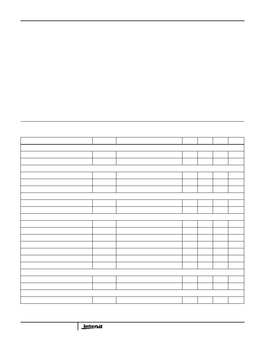
Electrical Specifications
Typical values are tested at VIN = 5V and 25įC Ambient Temperature, maximum and minimum values are
guaranteed over 0įC to 70įC Ambient Temperature with a supply voltage in the range of 4.3V to 6.5V, unless
otherwise noted.
PARAMETER
SYMBOL
TEST CONDITIONS
MIN
TYP
MAX
UNITS
POWER-ON RESET
Rising VIN Threshold
V
POR
3.0
3.5
4.0
V
Falling VIN Threshold (Note 3)
V
POR
2.25
2.4
2.65
V
STANDBY CURRENT
VBAT Pin Sink Current
I
STANDBY
VIN floating or EN = LOW
-
-
3.0
ĶA
VIN Pin Supply Current
I
VIN
VBAT floating and EN pulled low
-
30
-
ĶA
VIN Pin Supply Current
I
VIN
VBAT floating and EN floating
-
1
-
mA
VOLTAGE REGULATION
Output Voltage
V
CH
4.158
4.20
4.242
V
Dropout Voltage
VBAT = 3.7V, 0.5A
-
140
-
mV
CHARGE CURRENT
Constant Charge Current (Note 4)
I
CHARGE
R
IREF
= 80k
, V
BAT
= 3.7V
0.9
1.0
1.1
A
Trickle Charge Current
I
TRICKLE
R
IREF
= 80k
, V
BAT
= 2.0V
-
110
-
mA
Constant Charge Current
I
CHARGE
IREF Pin Voltage > 1.3V, V
BAT
= 3.7V
400
450
500
mA
Trickle Charge Current
I
TRICKLE
IREF Pin Voltage > 1.3V, V
BAT
= 2.0V
-
45
-
mA
Constant Charge Current
I
CHARGE
IREF Pin Voltage < 0.4V, V
BAT
= 3.7V
-
-
100
mA
Trickle Charge Current
I
TRICKLE
IREF Pin Voltage < 0.4V, V
BAT
= 2.0V
-
10
-
mA
End-of-Charge Threshold
R
IMIN
= 80k
85
110
135
mA
RECHARGE THRESHOLD
Recharge Voltage Threshold Below V
CH
V
RECHRG
The threshold in relative to V
CH
-
-200
-80
mV
Recharge Voltage Threshold
V
RECHRG
3.85
4.0
-
V
TRICKLE CHARGE THRESHOLD
Trickle Charge Threshold Voltage
V
MIN
2.56
2.76
3.0
V
ISL6292D

3
TEMPERATURE MONITORING
Low Battery Temperature Threshold
V
TMIN
V2P8 = 3.0V
1.40
1.50
1.60
V
Low Temperature Threshold Hysteresis
V2P8 = 3.0V
-
214
-
mV
High Battery Temperature Threshold
V
TMAX
V2P8 = 3.0V
.587
0.605
.623
V
High Temperature Threshold Hysteresis
V2P8 = 3.0V
-
55
-
mV
Battery Removal Threshold
V
RMV
V2P8 = 3.0V
-
2.25
-
V
Charge Current Foldback Threshold (Note 5)
T
FOLD
85
100
115
įC
Current Foldback Gain (Note 5)
G
FOLD
-
100
-
mA/įC
OSCILLATOR
Oscillation Period
T
OSC
C
TIME
= 15nF
2.4
3.0
3.6
ms
LOGIC INPUT AND OUTPUT
TOEN Input High
2.0
-
-
V
TOEN and EN Input Low
-
-
0.8
V
IREF and IMIN Input High
1.2
-
-
V
IREF and IMIN Input Low
-
-
0.4
V
STAT1/STAT2 Sink Current
Pin Voltage = 0.8V
5
-
-
mA
NOTES:
3. The POR falling edge voltage is guaranteed to be lower than the Trickle Charge Threshold Voltage (V
MIN
) by actual tests.
4. The actual charge current may be affected by the thermal foldback function if the thermal dissipation capability is not enough or by the on
resistance of the power MOSFET if the charger input voltage is too close to the output voltage.
5. Guaranteed by design, not a tested parameter.
Electrical Specifications
Typical values are tested at VIN = 5V and 25įC Ambient Temperature, maximum and minimum values are
guaranteed over 0įC to 70įC Ambient Temperature with a supply voltage in the range of 4.3V to 6.5V, unless
otherwise noted. (Continued)
PARAMETER
SYMBOL
TEST CONDITIONS
MIN
TYP
MAX
UNITS
ISL6292D

4
Pin Description
VIN (Pin 1, 15, 16)
VIN is the input power source. Connect to a wall adapter.
STAT2 (Pin 2)
STAT2 is an open-drain output to indicate the charger status.
This pin is pulled to LOW during charging and to HIGH when
not charging. When a fault situation occurs, the pin outputs a
one-speed blinking indication.
STAT1 (Pin 3)
STAT1 is an open-drain output to indicate the charger status.
The STAT1 pin is pulled LOW when the charger is charging
a battery and to HIGH when the charge finishes. This pin
outputs two different speeds of blinking signal depending on
the type of the fault case.
TIME (Pin 4)
The TIME pin determines the oscillation period by
connecting a timing capacitor between this pin and GND.
The oscillator also provides a time reference for the charger.
GND (Pin 5)
GND is the connection to system ground.
TOEN (Pin 6)
TOEN is the TIMEOUT enable input pin. Pulling this pin to
LOW disables the TIMEOUT charge-time limit for the fast
charge modes. Leaving this pin HIGH or floating enables the
TIMEOUT limit.
EN (Pin 7)
EN is the enable logic input. Connect the EN pin to LOW to
disable the charger or leave it floating to enable the charger.
V2P8 (Pin 8)
This is a 2.8V reference voltage output. This pin outputs a
2.8V voltage source when the input voltage is above POR
threshold and outputs zero otherwise. The V2P8 pin can be
used as an indication for adapter presence. Use a 1
ĶF
ceramic capacitor to stabilize the internal linear regulator.
IREF
(Pin 9)
This is the programming input for the constant charging
current.
IMIN (Pin 10)
IMIN is the programmable input for the end-of-charge
current.
TEMP (Pin 11)
TEMP is the input for an external NTC thermistor. The TEMP
pin is also used for battery removal detection.
VBAT (Pin 12, 13, 14)
VBAT is the connection to the battery. Typically a 10
ĶF
Tantalum capacitor is needed for stability when there is no
battery attached. When a battery is attached, only a 0.1
ĶF
ceramic capacitor is required as the minimum decoupling
capacitor.
Typical Application
V2P8
EN
GND
VBAT
IREF
STAT2
VIN
5V WALL
ADAPTER
BATTERY
PACK
IMIN
TEMP
STAT1
TIME
ISL6292D
V2P8
TOEN
T
C
1
10ĶF
330
R
1
C
2
1ĶF
R
T
R
U
C
3
R
IREF
80k
C
TIME
15nF
D
1
R
IMIN
80k
1ĶF
+
-
ISL6292D

5
Block Diagram
LOGIC
STAT1
EN
I
SEN
VIN
VBAT
100000:1
Current
Mirror
COUNTER
+
-
+
-
V
MIN
+
-
+
-
V
CH
IREF
+
-
IMIN
TEMP
STAT2
Recharge
Minbat
Under Temp
V
RECHRG
CA
VA
MIN_I
Input_OK
I
R
I
SEN
I
MIN
TOEN
V2P8
CHRG
+
-
+
-
Input_OK
V
POR
Trickle/Fast
References
V2P8
Temperature
Monitoring
Current
References
I
T
NTC
Interface
Over Temp
Batt Removal
TIME
OSC
GND
VIN
VBAT
V
CH
V
MIN
V
PO
R
V
R
E
CH
RG
Q
MAIN
Q
SEN
R
IREF
R
IMIN
C
1
+
100mV
-
VIN
VIN
FIGURE 1. BLOCK PROGRAM
ISL6292D