 | –≠–ª–µ–∫—Ç—Ä–æ–Ω–Ω—ã–π –∫–æ–º–ø–æ–Ω–µ–Ω—Ç: ISL6520B | –°–∫–∞—á–∞—Ç—å:  PDF PDF  ZIP ZIP |

1
Æ
FN9083.2
ISL6520B
Single Synchronous Buck Pulse-Width
Modulation (PWM) Controller
The ISL6520B makes simple work out of implementing a
complete control scheme for a DC-DC stepdown converter.
Designed to drive N-channel MOSFETs in a synchronous
buck topology, the ISL6520B integrates the control, output
adjustment and monitoring functions into a single 8-Lead
package.
The ISL6520B provides simple, single feedback loop,
voltage-mode control with fast transient response. The
output voltage can be precisely regulated to as low as 0.8V,
with a maximum tolerance of
±
1.5% over temperature and
line voltage variations. A fixed frequency oscillator reduces
design complexity, while balancing typical application cost
and efficiency.
The error amplifier features a 15MHz gain-bandwidth
product and 8V/
µ
s slew rate which enables high converter
bandwidth for fast transient performance. The resulting PWM
duty cycles range from 0% to 100%.
Pinouts
Features
∑ Operates from +5V Input
∑ 0.8V to V
IN
Output Range
- 0.8V Internal Reference
- ±1.5% Over Line Voltage and Temperature
∑ Drives N-Channel MOSFETs
∑ Simple Single-Loop Control Design
- Voltage-Mode PWM Control
∑ Fast Transient Response
- High-Bandwidth Error Amplifier
- Full 0% to 100% Duty Cycle
∑ Small Converter Size
- 300kHz Fixed Frequency Oscillator
- Internal Soft Start
- 8 Ld SOIC or 16Ld 4x4mm QFN
∑ QFN Package:
- Compliant to JEDEC PUB95 MO-220 QFN - Quad Flat
No Leads - Package Outline
- Near Chip Scale Package footprint, which improves
PCB efficiency and has a thinner profile
∑ Pb-Free Available (RoHS Compliant)
Applications
∑ Power Supplies for Microprocessors
- PCs
- Embedded Controllers
∑ Subsystem Power Supplies
- PCI/AGP/GTL+ Buses
- ACPI Power Control
- SSTL-2 and DDR SDRAM Bus Termination Supply
∑ Cable Modems, Set Top Boxes, and DSL Modems
∑ DSP and Core Communications Processor Supplies
∑ Memory Supplies
∑ Personal Computer Peripherals
∑ Industrial Power Supplies
∑ 5V-Input DC-DC Regulators
∑ Low-Voltage Distributed Power Supplies
5
6
8
7
4
3
2
1
UGATE
GND
PHASE
FB
VCC
COMP/SD
BOOT
LGATE
NC
COMP/SD
NC
FB
BOOT
UGATE
GND
NC
NC
NC
PHASE
NC
LG
A
T
E
NC
VCC
NC
ISL6520B (8 LD SOIC)
TOP VIEW
ISL6520B (16 LD QFN)
TOP VIEW
1
3
4
15
16
14
13
2
12
10
9
11
6
5
7
8
Data Sheet
January 20, 2005
CAUTION: These devices are sensitive to electrostatic discharge; follow proper IC Handling Procedures.
1-888-INTERSIL or 321-724-7143
|
Intersil (and design) is a registered trademark of Intersil Americas Inc.
Copyright © Intersil Americas Inc. 2003, 2005. All Rights Reserved
All other trademarks mentioned are the property of their respective owners.

2
FN9083.2
January 20, 2005
Block Diagram
Typical Application
Ordering Information
PART NUMBER
TEMP.
RANGE (
o
C)
PACKAGE
PKG.
DWG. #
ISL6520BCB
0 to 70
8 Ld SOIC
M8.15
ISL6520BCBZ
(See Note)
0 to 70
8 Ld SOIC
(Pb-free)
M8.15
ISL6520BCR
0 to 70
16 Ld 4x4 QFN
L16.4x4
ISL6520BCRZ
(See Note)
0 to 70
16 Ld 4x4 QFN
(Pb-free)
L16.4x4
ISL6520BIR
-40 to 85
16 Ld 4x4 QFN
L16.4x4
ISL6520BIRZ
(See Note)
-40 to 85
16 Ld 4x4 QFN
(Pb-free)
L16.4x4
ISL6520EVAL1
Evaluation Board
Add "-T" suffix for tape and reel.
NOTE: Intersil Pb-free products employ special Pb-free material sets; molding
compounds/die attach materials and 100% matte tin plate termination finish,
which are RoHS compliant and compatible with both SnPb and Pb-free
soldering operations. Intersil Pb-free products are MSL classified at Pb-free
peak reflow temperatures that meet or exceed the Pb-free requirements of
IPC/JEDEC J STD-020.
Ordering Information
(Continued)
PART NUMBER
TEMP.
RANGE (
o
C)
PACKAGE
PKG.
DWG. #
+
-
+
-
OSCILLATOR
INHIBIT
PWM
COMPARATOR
ERROR
AMP
V
CC
PWM
GND
FB
COMP/SD
0.8V
GATE
CONTROL
LOGIC
BOOT
UGATE
PHASE
20
µ
A
FIXED 300kHz
+
-
LGATE
VCC
SOFTSTART
POR AND
5V
V
OUT
FB
COMP/SD
UGATE
PHASE
BOOT
VCC
GND
LGATE
5
7
6
3
2
1
8
4
ISL6520B
R
S
R
OFFSET
C
I
C
F
R
F
L
OUT
D
BOOT
C
BOOT
C
BULK
C
DCPL
C
HF
C
OUT
V
IN
Q
U
Q
L
R
PULLUP
SHUTDOWN
ISL6520B
3
FN9083.2
January 20, 2005
Absolute Maximum Ratings
Thermal Information
Supply Voltage, V
CC
. . . . . . . . . . . . . . . . . . . . . . . . . . . . . . . . +6.0V
Absolute Boot Voltage, V
BOOT
. . . . . . . . . . . . . . . . . . . . . . . +15.0V
Upper Driver Supply Voltage, V
BOOT
- V
PHASE
. . . . . . . . . . . +6.0V
Input, Output or I/O Voltage . . . . . . . . . . . GND -0.3V to VCC +0.3V
ESD Classification . . . . . . . . . . . . . . . . . . . . . . . . . . . . . . . . . Class 2
Operating Conditions
Supply Voltage, VCC . . . . . . . . . . . . . . . . . . . . . . . . . . . . +5V ±10%
Ambient Temperature Range - ISL6520BC . . . . . . . . . . 0
o
C to 70
o
C
Junction Temperature Range . . . . . . . . . . . . . . . . . . -40
o
C to 125
o
C
Thermal Resistance
JA
(
o
C/W)
JC
(
o
C/W)
SOIC Package (Note 1) . . . . . . . . . . . . . .
95
N/A
QFN Package (Note 2, 3). . . . . . . . . . . . . .
45
7
Maximum Junction Temperature
(Plastic Package) . . . . . . . . . . . . . . . . . . . . . . . . . . . . . . . 150
o
C
Maximum Storage Temperature Range . . . . . . . . -65
o
C to 150
o
C
Maximum Lead Temperature
(Soldering 10s) . . . . . . . . . . . . . . . . . . . . . . . . . . . . . . . . . 300
o
C
(SOIC - Lead Tips Only)
CAUTION: Stresses above those listed in "Absolute Maximum Ratings" may cause permanent damage to the device. This is a stress only rating and operation of the
device at these or any other conditions above those indicated in the operational sections of this specification is not implied.
NOTES:
1.
JA
is measured with the component mounted on a high effective thermal conductivity test board in free air. See Tech Brief TB379 for details.
2.
JA
is measured in free air with the component mounted on a high effective thermal conductivity test board with "direct attach" features. See
Tech Brief TB379.
3. For
JC
, the "case temp" location is the center of the exposed metal pad on the package underside.
Electrical Specifications
Recommended Operating Conditions, Unless Otherwise Noted.
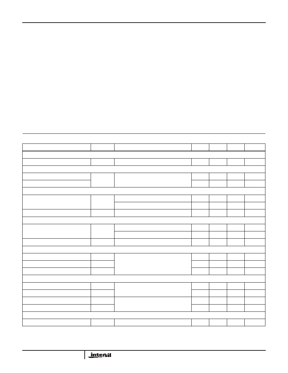
PARAMETER
SYMBOL
TEST CONDITIONS
MIN
TYP
MAX
UNITS
VCC SUPPLY CURRENT
Nominal Supply
I
VCC
2.6
3.2
3.8
mA
POWER-ON RESET
Rising VCC POR Threshold
POR
4.19
4.30
4.50
V
VCC POR Threshold Hysteresis
-
0.25
-
V
OSCILLATOR
Frequency
f
OSC
ISL6520BC, VCC
= 5V
250
300
340
kHz
ISL6520BI, VCC
= 5V
230
300
340
kHz
Ramp Amplitude
V
OSC
-
1.5
-
V
P-P
REFERENCE
Reference Voltage Tolerance
ISL6520BC
-1.5
-
+1.5
%
ISL6520BI
-2.5
+2.5
%
Nominal Reference Voltage
V
REF
-
0.800
-
V
ERROR AMPLIFIER
DC Gain
Guaranteed By Design
-
88
-
dB
Gain-Bandwidth Product
GBWP
-
15
-
MHz
Slew Rate
SR
-
8
-
V/
µ
s
GATE DRIVERS
Upper Gate Source Current
I
UGATE-SRC
V
BOOT
- V
PHASE
= 5V, V
UGATE
= 4V
-
-1
-
A
Upper Gate Sink Current
I
UGATE-SNK
-
1
-
A
Lower Gate Source Current
I
LGATE-SRC
V
VCC
= 5V, V
LGATE
= 4V
-
-1
-
A
Lower Gate Sink Current
I
LGATE-SNK
-
2
-
A
DISABLE
Disable Threshold
V
DISABLE
-
0.8
-
V
ISL6520B
4
FN9083.2
January 20, 2005
Functional Pin Description
VCC
This pin provides the bias supply for the ISL6520B, as well
as the lower MOSFET's gate. Connect a well-decoupled 5V
supply to this pin.
FB
This pin is the inverting input of the internal error amplifier.
Use this pin, in combination with the COMP/SD pin, to
compensate the voltage-control feedback loop of the
converter.
GND
This pin represents the signal and power ground for the IC.
Tie this pin to the ground island/plane through the lowest
impedance connection available.
PHASE
Connect this pin to the upper MOSFET's source.
UGATE
Connect this pin to the upper MOSFET's gate. This pin
provides the PWM-controlled gate drive for the upper
MOSFET. This pin is also monitored by the adaptive shoot-
through protection circuitry to determine when the upper
MOSFET has turned off.
BOOT
This pin provides ground referenced bias voltage to the
upper MOSFET driver. A bootstrap circuit is used to create a
voltage suitable to drive a logic-level N-channel MOSFET.
COMP/SD
This pin is the output of the error amplifier. Use this pin, in
combination with the FB pin, to compensate the voltage-
control feedback loop of the converter.
Pulling COMP/SD to a level below 0.8V disables the
controller. Disabling the ISL6520B causes the oscillator to
stop, the LGATE and UGATE outputs to be held low, and the
softstart circuitry to re-arm. The COMP/SD pin must be
pulled above 0.8V to terminate shutdown. This may be done
through a pullup resistor tied between VCC and COMP/SD.
The recommended range of resistor values to use as the pullup
resistor is between 50k
and 100k
.
LGATE
Connect this pin to the lower MOSFET's gate. This pin
provides the PWM-controlled gate drive for the lower
MOSFET. This pin is also monitored by the adaptive shoot-
through protection circuitry to determine when the lower
MOSFET has turned off.
Functional Description
Initialization
The ISL6520B automatically initializes upon receipt of power.
The Power-On Reset (POR) function continually monitors the
bias voltage at the VCC pin. The POR function initiates the soft
start operation.
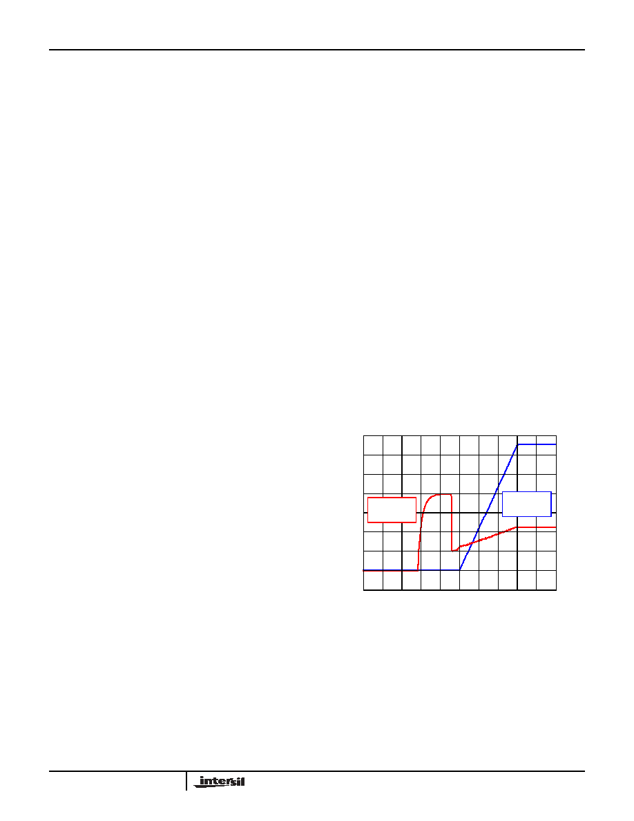
Soft Start
The ISL6520B is held in reset with both UGATE and LGATE
driven to ground until the POR threshold on VCC has been
reached and the COMP/SD pin has been pulled above 0.8V. If
COMP is not actively pulled high following POR the internal
20
µ
A current sink will hold COMP/SD low and the device will
remain in reset. COMP/SD can either be statically tied to VCC
through a pullup resistor or driven high through a resistor to
terminate reset. The recommended range of resistor values to
use as the pullup resistor is between 50k
and 100k
.
Following reset the ISL6520B provides a 1024 clock cycle
settling period (~3.4ms) prior to initiating softstart. At the
conclusion of the settling period the COMP/SD pin is driven
to 0.8V for 24 clock cycles (~75
µ
s) to discharge the
compensation network. Soft start of the regulated output is
generated by imposing an internal offset on the FB pin which
ramps down from 0.8V to 0V over the next 2048 clock cycles
(~6.8ms). Total time from end of reset to completion of soft start
is 10.2ms.
Pulling COMP/SD below.8V or VCC dropping below
minimum POR initiates another reset.
Current Sinking
The ISL6520B incorporates a MOSFET shoot-through
protection method which allows a converter to sink current
as well as source current. Care should be exercised when
designing a converter with the ISL6520B when it is known
that the converter may sink current.
When the converter is sinking current, it is behaving as a
boost converter that is regulating it's input voltage. This
means that the converter is boosting current into the V
CC
FIGURE 1. SOFT START INTERVAL
TIME (2ms/DIV.)
V
OUT
500mV/DIV.
V
COMP/SD
1V/DIV.
ISL6520B

5
FN9083.2
January 20, 2005
rail, which supplies the bias voltage to the ISL6520B. If there
is nowhere for this current to go, such as to other distributed
loads on the V
CC
rail, through a voltage limiting protection
device, or other methods, the capacitance on the V
CC
bus
will absorb the current. This situation will allow voltage level
of the V
CC
rail to increase. If the voltage level of the rail is
boosted to a level that exceeds the maximum voltage rating
of the ISL6520B, then the IC will experience an irreversible
failure and the converter will no longer be operational.
Ensuring that there is a path for the current to follow other
than the capacitance on the rail will prevent this failure mode.
Application Guidelines
Layout Considerations
As in any high frequency switching converter, layout is very
important. Switching current from one power device to another
can generate voltage transients across the impedances of the
interconnecting bond wires and circuit traces. These
interconnecting impedances should be minimized by using
wide, short printed circuit traces. The critical components
should be located as close together as possible, using ground
plane construction or single point grounding.
Figure 2 shows the critical power components of the converter.
To minimize the voltage overshoot, the interconnecting wires
indicated by heavy lines should be part of a ground or power
plane in a printed circuit board. The components shown in
Figure 2 should be located as close together as possible.
Please note that the capacitors C
IN
and C
O
may each
represent numerous physical capacitors. Locate the
ISL6520B
within 3 inches of the MOSFETs, Q
1
and Q
2
. The circuit traces
for the MOSFETs' gate and source connections from the
ISL6520B must be sized to handle up to 1A peak current.
Figure 3 shows the circuit traces that require additional
layout consideration. Use single point and ground plane
construction for the circuits shown. Minimize any leakage
current paths on the COMP/SD pin and locate the resistor,
R
OSCET
close to the COMP/SD pin because the internal
current source is only 20
µ
A. Provide local V
CC
decoupling
between VCC and GND pins. Locate the capacitor, C
BOOT
as close as practical to the BOOT and PHASE pins. All
components used for feedback compensation should be
located as close to the IC a practical.
Feedback Compensation
Figure 4 highlights the voltage-mode control loop for a
synchronous-rectified buck converter. The output voltage
(V
OUT
) is regulated to the Reference voltage level. The
error amplifier (Error Amp) output (V
E/A
) is compared with
the oscillator (OSC) triangular wave to provide a
pulse-width modulated (PWM) wave with an amplitude of
V
IN
at the PHASE node. The PWM wave is smoothed by the
output filter (L
O
and C
O
).
The modulator transfer function is the small-signal transfer
function of V
OUT
/V
E/A
. This function is dominated by a DC
Gain and the output filter (L
O
and C
O
), with a double pole
L
O
C
O
LGATE
UGATE
PHASE
Q
1
Q
2
V
IN
V
OUT
RETURN
ISL6520B
C
IN
LO
AD
FIGURE 2. PRINTED CIRCUIT BOARD POWER AND
GROUND PLANES OR ISLANDS
FIGURE 3. PRINTED CIRCUIT BOARD SMALL SIGNAL
LAYOUT GUIDELINES
+5V
ISL6520B
GND
VCC
BOOT
D
1
L
O
C
O
V
OUT
LO
AD
Q
1
Q
2
PHASE
+V
IN
C
BOOT
C
VCC
FIGURE 4. VOLTAGE-MODE BUCK CONVERTER
COMPENSATION DESIGN
V
OUT
REFERENCE
L
O
C
O
ESR
V
IN
V
OSC
ERROR
AMP
PWM
DRIVER
(PARASITIC)
Z
FB
+
-
REFERENCE
R
1
R
3
R
2
C
3
C
2
C
1
COMP/SD
V
OUT
FB
Z
FB
ISL6520B
Z
IN
COMPARATOR
DRIVER
DETAILED COMPENSATION COMPONENTS
PHASE
V
E/A
+
-
+
-
Z
IN
OSC
ISL6520B
6
FN9083.2
January 20, 2005
break frequency at F
LC
and a zero at F
ESR
. The DC Gain of
the modulator is simply the input voltage (V
IN
) divided by the
peak-to-peak oscillator voltage
V
OSC
.
Modulator Break Frequency Equations
The compensation network consists of the error amplifier
(internal to the ISL6520B) and the impedance networks Z
IN
and Z
FB
. The goal of the compensation network is to provide
a closed loop transfer function with the highest 0dB crossing
frequency (f
0dB
) and adequate phase margin. Phase margin
is the difference between the closed loop phase at f
0dB
and
180 degrees. The equations below relate the compensation
network's poles, zeros and gain to the components (R
1
, R
2
,
R
3
, C
1
, C
2
, and C
3
) in Figure 4. Use these guidelines for
locating the poles and zeros of the compensation network:
1. Pick Gain (R
2
/R
1
) for desired converter bandwidth.
2. Place 1
ST
Zero Below Filter's Double Pole (~75% F
LC
).
3. Place 2
ND
Zero at Filter's Double Pole.
4. Place 1
ST
Pole at the ESR Zero.
5. Place 2
ND
Pole at Half the Switching Frequency.
6. Check Gain against Error Amplifier's Open-Loop Gain.
7. Estimate Phase Margin - Repeat if Necessary.
Compensation Break Frequency Equations
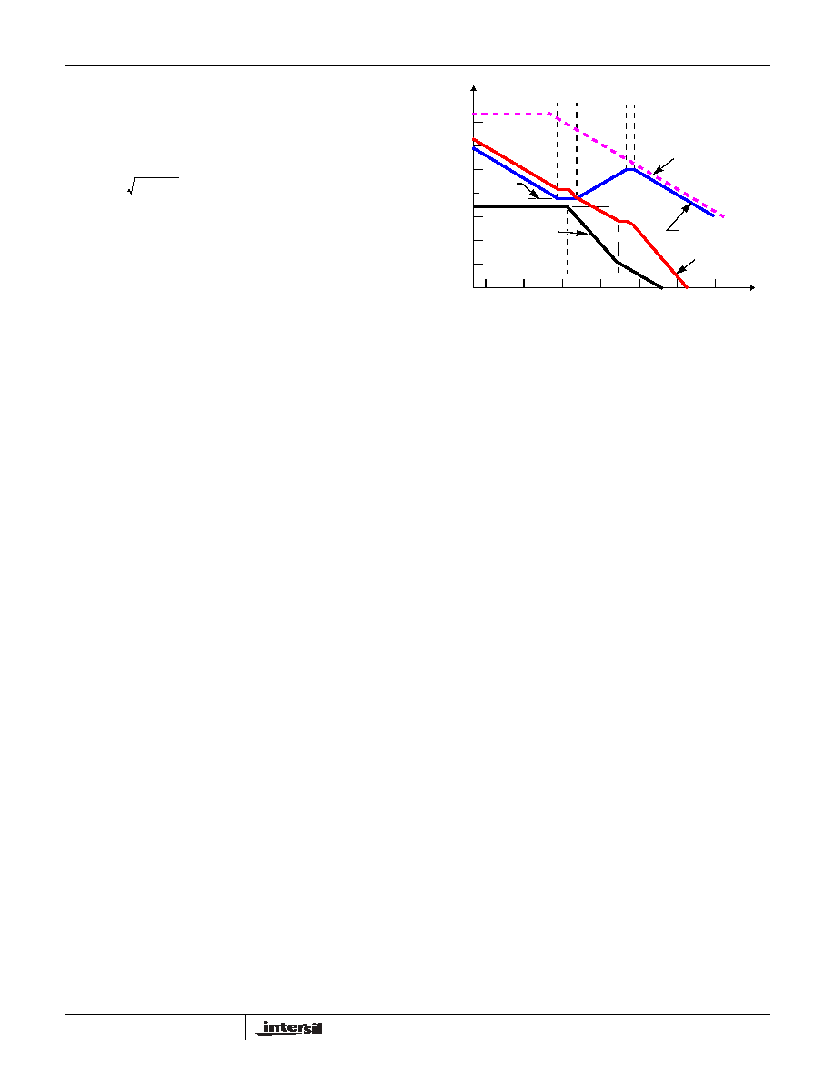
Figure 5 shows an asymptotic plot of the DC-DC converter's
gain vs frequency. The actual Modulator Gain has a high gain
peak due to the high Q factor of the output filter and is not
shown in Figure 5. Using the above guidelines should give a
Compensation Gain similar to the curve plotted. The open
loop error amplifier gain bounds the compensation gain.
Check the compensation gain at F
P2
with the capabilities of
the error amplifier. The Closed Loop Gain is constructed on
the graph of Figure 5 by adding the Modulator Gain (in dB) to
the Compensation Gain (in dB). This is equivalent to
multiplying the modulator transfer function to the
compensation transfer function and plotting the gain.
The compensation gain uses external impedance networks
Z
FB
and Z
IN
to provide a stable, high bandwidth (BW) overall
loop. A stable control loop has a gain crossing with
-20dB/decade slope and a phase margin greater than 45
degrees. Include worst case component variations when
determining phase margin.
Component Selection Guidelines
Output Capacitor Selection
An output capacitor is required to filter the output and supply
the load transient current. The filtering requirements are a
function of the switching frequency and the ripple current.
The load transient requirements are a function of the slew
rate (di/dt) and the magnitude of the transient load current.
These requirements are generally met with a mix of
capacitors and careful layout.
Modern components and loads are capable of producing
transient load rates above 1A/ns. High frequency capacitors
initially supply the transient and slow the current load rate
seen by the bulk capacitors. The bulk filter capacitor values
are generally determined by the ESR (Effective Series
Resistance) and voltage rating requirements rather than
actual capacitance requirements.
High frequency decoupling capacitors should be placed as
close to the power pins of the load as physically possible. Be
careful not to add inductance in the circuit board wiring that
could cancel the usefulness of these low inductance
components. Consult with the manufacturer of the load on
specific decoupling requirements.
Use only specialized low-ESR capacitors intended for
switching-regulator applications for the bulk capacitors. The
bulk capacitor's ESR will determine the output ripple voltage
and the initial voltage drop after a high slew-rate transient. An
aluminum electrolytic capacitor's ESR value is related to the
case size with lower ESR available in larger case sizes.
However, the Equivalent Series Inductance (ESL) of these
capacitors increases with case size and can reduce the
usefulness of the capacitor to high slew-rate transient loading.
Unfortunately, ESL is not a specified parameter. Work with
your capacitor supplier and measure the capacitor's
impedance with frequency to select a suitable component. In
most cases, multiple electrolytic capacitors of small case size
perform better than a single large case capacitor.
FLC
1
2
x LO x CO
-------------------------------------------
=
FESR
1
2
x ESR x CO
--------------------------------------------
=
F
Z1
1
2
x R
2
x C
1
------------------------------------
=
F
Z2
1
2
x R
1
R
3
+
(
) x C
3
-------------------------------------------------------
=
F
P1
1
2
x R
2
x
C
1
x C
2
C
1
C
2
+
----------------------
---------------------------------------------------------
=
F
P2
1
2
x R
3
x C
3
------------------------------------
=
100
80
60
40
20
0
-20
-40
-60
F
P1
F
Z2
10M
1M
100K
10K
1K
100
10
OPEN LOOP
ERROR AMP GAIN
F
Z1
F
P2
20LOG
F
LC
F
ESR
COMPENSATION
GA
IN (
d
B)
FREQUENCY (Hz)
GAIN
20LOG
(V
IN
/
V
OSC
)
MODULATOR
GAIN
(R
2
/R
1
)
FIGURE 5. ASYMPTOTIC BODE PLOT OF CONVERTER GAIN
CLOSED LOOP
GAIN
ISL6520B

7
FN9083.2
January 20, 2005
Output Inductor Selection
The output inductor is selected to meet the output voltage
ripple requirements and minimize the converter's response
time to the load transient. The inductor value determines the
converter's ripple current and the ripple voltage is a function
of the ripple current. The ripple voltage and current are
approximated by the following equations:
Increasing the value of inductance reduces the ripple current
and voltage. However, the large inductance values reduce
the converter's response time to a load transient.
One of the parameters limiting the converter's response to
a load transient is the time required to change the inductor
current. Given a sufficiently fast control loop design, the
ISL6520B will provide either 0% or 100% duty cycle in
response to a load transient. The response time is the time
required to slew the inductor current from an initial current
value to the transient current level. During this interval the
difference between the inductor current and the transient
current level must be supplied by the output capacitor.
Minimizing the response time can minimize the output
capacitance required.
The response time to a transient is different for the
application of load and the removal of load. The following
equations give the approximate response time interval for
application and removal of a transient load:
where: I
TRAN
is the transient load current step, t
RISE
is the
response time to the application of load, and t
FALL
is the
response time to the removal of load. The worst case
response time can be either at the application or removal of
load. Be sure to check both of these equations at the
minimum and maximum output levels for the worst case
response time.
Input Capacitor Selection
Use a mix of input bypass capacitors to control the voltage
overshoot across the MOSFETs. Use small ceramic
capacitors for high frequency decoupling and bulk capacitors
to supply the current needed each time Q
1
turns on. Place the
small ceramic capacitors physically close to the MOSFETs
and between the drain of Q
1
and the source of Q
2
.
The important parameters for the bulk input capacitor are the
voltage rating and the RMS current rating. For reliable
operation, select the bulk capacitor with voltage and current
ratings above the maximum input voltage and largest RMS
current required by the circuit. The capacitor voltage rating
should be at least 1.25 times greater than the maximum
input voltage and a voltage rating of 1.5 times is a
conservative guideline. The RMS current rating requirement
for the input capacitor of a buck regulator is approximately
1/2 the DC load current.
For a through hole design, several electrolytic capacitors may
be needed. For surface mount designs, solid tantalum
capacitors can be used, but caution must be exercised with
regard to the capacitor surge currentrating. These capacitors
must be capable of handling the surge-current at power-up.
Some capacitor series available from reputable manufacturers
are surge current tested.
MOSFET Selection/Considerations
The ISL6520B requires 2 N-Channel power MOSFETs. These
should be selected based upon r
DS(ON)
, gate supply
requirements, and thermal management requirements.
In high-current applications, the MOSFET power dissipation,
package selection and heatsink are the dominant design
factors. The power dissipation includes two loss components;
conduction loss and switching loss. The conduction losses are
the largest component of power dissipation for both the upper
and the lower MOSFETs. These losses are distributed between
the two MOSFETs according to duty factor. The switching
losses seen when sourcing current will be different from the
switching losses seen when sinking current. When sourcing
current, the upper MOSFET realizes most of the switching
losses. The lower switch realizes most of the switching
losses when the converter is sinking current (see the
equations below). These equations assume linear voltage-
current transitions and do not adequately model power loss
due the reverse-recovery of the upper and lower MOSFET's
body diode. The gate-charge losses are dissipated by the
ISL6520B
and don't heat the MOSFETs. However, large gate-
charge increases the switching interval, t
SW
which increases
the MOSFET switching losses. Ensure that both MOSFETs
are within their maximum junction temperature at high ambient
temperature by calculating the temperature rise according to
package thermal-resistance specifications. A separate heatsink
may be necessary depending upon MOSFET power, package
type, ambient temperature and air flow.
Given the reduced available gate bias voltage (5V),
logic-level or sub-logic-level transistors should be used for
both N-MOSFETs. Caution should be exercised with devices
exhibiting very low V
GS(ON)
characteristics. The shoot-
through protection present aboard the ISL6520B may be
I
=
V
IN
- V
OUT
Fs x L
V
OUT
V
IN
V
OUT
=
I
x
ESR
x
t
RISE
=
L x I
TRAN
V
IN
- V
OUT
t
FALL
=
L x I
TRAN
V
OUT
P
LOWER
= Io
2
x r
DS(ON)
x (1 - D)
Where: D is the duty cycle = V
OUT
/ V
IN
,
t
SW
is the combined switch ON and OFF time, and
F
S
is the switching frequency.
Losses while Sourcing Current
Losses while Sinking Current
P
LOWER
Io
2
r
DS ON
(
)
◊
1 D
≠
(
)
◊
1
2
---
Io
V
IN
◊
t
SW
F
S
◊
◊
+
=
P
UPPER
Io
2
r
DS ON
(
)
◊
D
◊
1
2
---
Io
V
IN
◊
t
SW
F
S
◊
◊
+
=
P
UPPER
= Io
2
x r
DS(ON)
x D
ISL6520B

8
FN9083.2
January 20, 2005
circumvented by these MOSFETs if they have large parasitic
impedences and/or capacitances that would inhibit the gate
of the MOSFET from being discharged below it's threshold
level before the complementary MOSFET is turned on.
Figure 6 shows the upper gate drive (BOOT pin) supplied by a
bootstrap circuit from V
CC
. The boot capacitor, C
BOOT
,
develops a floating supply voltage referenced to the PHASE
pin. The supply is refreshed to a voltage of V
CC
less the boot
diode drop (V
D
) each time the lower MOSFET, Q
2
, turns on.
ISL6520B DC-DC Converter Application
Circuit
Figure 7 shows an application circuit of a DC-DC Converter.
Detailed information on the circuit, including a complete Bill-
of-Materials and circuit board description, can be found in
Application Note AN9932.
+5V
ISL6520B
GND
LGATE
UGATE
PHASE
BOOT
VCC
+5V
NOTE:
NOTE:
V
G-S
V
CC
C
BOOT
D
BOOT
Q1
Q2
+
-
FIGURE 6. UPPER GATE DRIVE BOOTSTRAP
V
G-S
V
CC
-V
D
+ V
D
-
Component Selection Notes:
C
IN
-
Each 330
m
F 6.3W
VDC
, Sanyo 6TPB330M or Equivalent.
C
OUT
-
Each 330
m
F 6.3W
VDC
, Sanyo 6TPB330M or Equivalent.
D1 - 30mA Schottky Diode, MA732 or Equivalent
L
1
- 3.1
µH Inductor, Panasonic P/N ETQ-P6F2ROLFA or Equivalent.
Q
1
, Q
2
-
Fairchild MOSFET; HUF76143.
FIGURE 7. 5V to 3.3V 15A DC-DC CONVERTER
+5V
V
OUT
FB
COMP/SD
UGATE
PHASE
BOOT
VCC
GND
LGATE
+
5
7
6
3
2
1
8
4
ISL6520B
+
3.16k
L
1
C
OUT
D
1
0.1
µF
C
IN
2 x 1
µF
Q
1
Q
2
U
1
0.1
µF
POR
REF
OSC
+
-
-
+
3 x 330
µF
2 x 330
µF
0.1
µF
1.00k
10.0k
470pF
8200pF
60.4
18000pF
AND
SOFT START
50k
ISL6520B

9
FN9083.2
January 20, 2005
ISL6520B
Small Outline Plastic Packages (SOIC)
INDEX
AREA
E
D
N
1
2
3
-B-
0.25(0.010)
C A
M
B S
e
-A-
L
B
M
-C-
A1
A
SEATING PLANE
0.10(0.004)
h x 45
o
C
H
µ
0.25(0.010)
B
M
M
NOTES:
1. Symbols are defined in the "MO Series Symbol List" in Section 2.2 of
Publication Number 95.
2. Dimensioning and tolerancing per ANSI Y14.5M-1982.
3. Dimension "D" does not include mold flash, protrusions or gate burrs.
Mold flash, protrusion and gate burrs shall not exceed 0.15mm (0.006
inch) per side.
4. Dimension "E" does not include interlead flash or protrusions. Inter-
lead flash and protrusions shall not exceed 0.25mm (0.010 inch) per
side.
5. The chamfer on the body is optional. If it is not present, a visual index
feature must be located within the crosshatched area.
6. "L" is the length of terminal for soldering to a substrate.
7. "N" is the number of terminal positions.
8. Terminal numbers are shown for reference only.
9. The lead width "B", as measured 0.36mm (0.014 inch) or greater
above the seating plane, shall not exceed a maximum value of
0.61mm (0.024 inch).
10. Controlling dimension: MILLIMETER. Converted inch dimensions
are not necessarily exact.
M8.15
(JEDEC MS-012-AA ISSUE C)
8 LEAD NARROW BODY SMALL OUTLINE PLASTIC
PACKAGE
SYMBOL
INCHES
MILLIMETERS
NOTES
MIN
MAX
MIN
MAX
A
0.0532
0.0688
1.35
1.75
-
A1
0.0040
0.0098
0.10
0.25
-
B
0.013
0.020
0.33
0.51
9
C
0.0075
0.0098
0.19
0.25
-
D
0.1890
0.1968
4.80
5.00
3
E
0.1497
0.1574
3.80
4.00
4
e
0.050 BSC
1.27 BSC
-
H
0.2284
0.2440
5.80
6.20
-
h
0.0099
0.0196
0.25
0.50
5
L
0.016
0.050
0.40
1.27
6
N
8
8
7
0
o
8
o
0
o
8
o
-
Rev. 0 12/93

10
All Intersil U.S. products are manufactured, assembled and tested utilizing ISO9000 quality systems.
Intersil Corporation's quality certifications can be viewed at www.intersil.com/design/quality
Intersil products are sold by description only. Intersil Corporation reserves the right to make changes in circuit design, software and/or specifications at any time without
notice. Accordingly, the reader is cautioned to verify that data sheets are current before placing orders. Information furnished by Intersil is believed to be accurate and
reliable. However, no responsibility is assumed by Intersil or its subsidiaries for its use; nor for any infringements of patents or other rights of third parties which may result
from its use. No license is granted by implication or otherwise under any patent or patent rights of Intersil or its subsidiaries.
For information regarding Intersil Corporation and its products, see www.intersil.com
FN9083.2
January 20, 2005
ISL6520B
Quad Flat No-Lead Plastic Package (QFN)
Micro Lead Frame Plastic Package (MLFP)
L16.4x4
16 LEAD QUAD FLAT NO-LEAD PLASTIC PACKAGE
(COMPLIANT TO JEDEC MO-220-VGGC ISSUE C)
SYMBOL
MILLIMETERS
NOTES
MIN
NOMINAL
MAX
A
0.80
0.90
1.00
-
A1
-
-
0.05
-
A2
-
-
1.00
9
A3
0.20 REF
9
b
0.23
0.28
0.35
5, 8
D
4.00 BSC
-
D1
3.75 BSC
9
D2
1.95
2.10
2.25
7, 8
E
4.00 BSC
-
E1
3.75 BSC
9
E2
1.95
2.10
2.25
7, 8
e
0.65 BSC
-
k
0.25
-
-
-
L
0.50
0.60
0.75
8
L1 -
-
0.15
10
N
16
2
Nd
4
3
Ne
4
3
P
-
-
0.60
9
-
-
12
9
Rev. 5 5/04
NOTES:
1. Dimensioning and tolerancing conform to ASME Y14.5-1994.
2. N is the number of terminals.
3. Nd and Ne refer to the number of terminals on each D and E.
4. All dimensions are in millimeters. Angles are in degrees.
5. Dimension b applies to the metallized terminal and is measured
between 0.15mm and 0.30mm from the terminal tip.
6. The configuration of the pin #1 identifier is optional, but must be
located within the zone indicated. The pin #1 identifier may be
either a mold or mark feature.
7. Dimensions D2 and E2 are for the exposed pads which provide
improved electrical and thermal performance.
8. Nominal dimensions are provided to assist with PCB Land Pattern
Design efforts, see Intersil Technical Brief TB389.
9. Features and dimensions A2, A3, D1, E1, P &
are present when
Anvil singulation method is used and not present for saw
singulation.
10. Depending on the method of lead termination at the edge of the
package, a maximum 0.15mm pull back (L1) maybe present. L
minus L1 to be equal to or greater than 0.3mm.