 | –≠–ª–µ–∫—Ç—Ä–æ–Ω–Ω—ã–π –∫–æ–º–ø–æ–Ω–µ–Ω—Ç: ISL83384E | –°–∫–∞—á–∞—Ç—å:  PDF PDF  ZIP ZIP |
1
Æ
FN6017.1
CAUTION: These devices are sensitive to electrostatic discharge; follow proper IC Handling Procedures.
1-888-INTERSIL or 321-724-7143
|
Intersil (and design) is a registered trademark of Intersil Americas Inc.
Copyright © Intersil Americas Inc. 2003. All Rights Reserved
All other trademarks mentioned are the property of their respective owners.
ISL83384E
±
15kV ESD Protected, +3V to +5.5V,
1 Microamp, 250Kbps, RS-232
Transmitter/Receiver
The Intersil ISL83384E contains 3.0V to 5.5V powered
RS-232 transmitters/receivers which meet ElA/TIA-232 and
V.28/V.24 specifications, even at V
CC
= 3.0V. Targeted
applications are PDAs, Palmtops, and notebook and laptop
computers where the low operational, and even lower
standby, power consumption is critical. Efficient on-chip
charge pumps, coupled with a manual powerdown function
reduces the standby supply current to a 1
µ
A trickle. Small
footprint packaging, and the use of small, low value
capacitors ensure board space savings as well. Data rates
greater than 250Kbps are guaranteed at worst case load
conditions. This device is fully compatible with 3.3V only
systems, mixed 3.3V and 5.0V systems, and 5.0V only
systems.
The single pin powerdown function (SHDN = 0) disables all
the transmitters and receivers, while shutting down the
charge pump to minimize supply current drain.
Table 1 summarizes the features of the ISL83384E, while
Application Note AN9863 summarizes the features of each
device comprising the ICL32XX 3V family.
Features
∑ ESD Protection for RS-232 I/O Pins to
±
15kV (IEC61000)
∑ Drop In Replacement for MAX3384E, SP385E
∑ Low Power, Pin Compatible Upgrade for 5V MAX222,
SP310E, ADM222, and LT1780
∑ Single SHDN Pin Disables Transmitters and Receivers
∑ Meets EIA/TIA-232 and V.28/V.24 Specifications at 3V
∑ RS-232 Compatible with V
CC
= 2.7V
∑ Latch-Up Free
∑ On-Chip Voltage Converters Require Only Four External
0.1
µ
F Capacitors
∑ Receiver Hysteresis For Improved Noise Immunity
∑ Very Low Supply Current . . . . . . . . . . . . . . . . . . . . 0.3mA
∑ Guaranteed Minimum Data Rate . . . . . . . . . . . . 250Kbps
∑ Guaranteed Minimum Slew Rate . . . . . . . . . . . . . . . 6V/
µ
s
∑ Wide Power Supply Range . . . . . . . Single +3V to +5.5V
∑ Low Supply Current in Powerdown State. . . . . . . . . < 1
µ
A
Applications
∑ Any System Requiring RS-232 Communication Ports
- Battery Powered, Hand-Held, and Portable Equipment
- Laptop Computers, Notebooks, Palmtops
- Modems, Printers and other Peripherals
- Digital Cameras
- Cellular/Mobile Phones
Related Literature
∑ Technical Brief TB363 "Guidelines for Handling and
Processing Moisture Sensitive Surface Mount Devices
(SMDs)"
∑ AN9863, "3V to +5.5V, 250k-1Mbps, RS-232
Transmitters/Receivers"
Ordering Information
PART NUMBER
TEMP.
RANGE (
o
C)
PACKAGE
PKG. NO.
ISL83384ECB
0 to 70
18 Ld SOIC
M18.3
ISL83384ECB-T
0 to 70
Tape and Reel
M18.3
ISL83384ECA
0 to 70
20 Ld SSOP
M20.209
ISL83384ECA-T
0 to 70
Tape and Reel
M20.209
ISL83384EIA
-40 to 85
20 Ld SSOP
M20.209
ISL83384EIA-T
-40 to 85
Tape and Reel
M20.209
TABLE 1. SUMMARY OF FEATURES
PART
NUMBER
NO. OF
Tx.
NO. OF
Rx.
NO. OF
MONITOR Rx.
(R
OUTB
)
DATA
RATE
(Kbps)
Rx. ENABLE
FUNCTION?
READY
OUTPUT?
MANUAL
POWER-
DOWN?
AUTOMATIC
POWERDOWN
FUNCTION?
ISL83384E
2
2
0
250
NO
NO
YES
NO
Data Sheet
April 2003
2
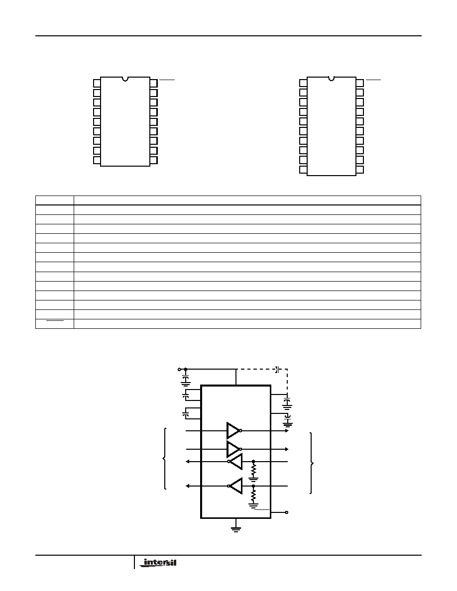
Pinouts
ISL83384E (SOIC)
TOP VIEW
ISL83384E (SSOP)
TOP VIEW
NC
C1+
V+
C1-
C2+
C2-
V-
T2
OUT
R2
IN
SHDN
GND
T1
OUT
R1
IN
R1
OUT
T2
IN
V
CC
T1
IN
R2
OUT
18
17
16
15
14
13
12
11
10
1
2
3
4
5
6
7
8
9
NC
C1+
V+
C1-
C2+
C2-
V-
T2
OUT
R2
IN
SHDN
GND
T1
OUT
R1
IN
R1
OUT
T2
IN
NC
V
CC
T1
IN
R2
OUT
20
19
18
17
16
15
14
13
12
11
1
2
3
4
5
6
7
8
9
10
NC
Pin Descriptions
PIN
FUNCTION
V
CC
System power supply input (3.0V to 5.5V).
V+
Internally generated positive transmitter supply (+5.5V).
V-
Internally generated negative transmitter supply (-5.5V).
GND
Ground connection.
C1+
External capacitor (voltage doubler) is connected to this lead.
C1-
External capacitor (voltage doubler) is connected to this lead.
C2+
External capacitor (voltage inverter) is connected to this lead.
C2-
External capacitor (voltage inverter) is connected to this lead.
T
IN
TTL/CMOS compatible transmitter Inputs.
T
OUT
±
15kV ESD Protected
,
RS-232 level (nominally
±
5.5V) transmitter outputs.
R
IN
±
15kV ESD Protected
,
RS-232 compatible receiver inputs.
R
OUT
TTL/CMOS level receiver outputs.
SHDN
Active low input to shut down transmitters, receivers, and on-board power supply, to place device in low power mode.
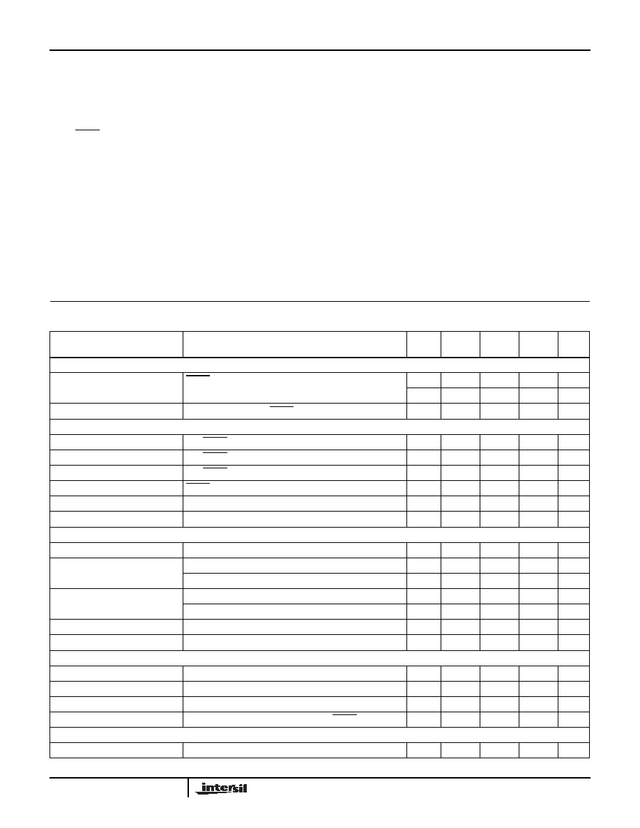
Typical Operating Circuits
ISL83384E (NOTE 2)
17
V
CC
T1
OUT
T2
OUT
T1
IN
T2
IN
T
1
T
2
0.1
µ
F
+
0.1
µ
F
+
0.1
µ
F
12
11
15
8
2
4
3
7
V+
V-
C1+
C1-
C2+
C2-
+
0.1
µ
F
5
6
R1
OUT
R1
IN
14
5k
R2
OUT
R2
IN
9
10
5k
13
C
1
C
2
+ C
3
C
4
SHDN
GND
18
+3.3V to +5V
+
0.1
µ
F
16
V
CC
TTL/CMOS
LOGIC LEVELS
RS-232
LEVELS
R
1
R
2
+
C
3
(OPTIONAL CONNECTION, NOTE 1)
NOTES:
1. The negative terminal of C
3
can be connected to either V
CC
or GND.
2. Pin numbers refer to SOIC package.
ISL83384E
3
Absolute Maximum Ratings
Thermal Information
V
CC
to Ground. . . . . . . . . . . . . . . . . . . . . . . . . . . . . . . . -0.3V to 6V
V+ to Ground . . . . . . . . . . . . . . . . . . . . . . . . . . . . . . . . . -0.3V to 7V
V- to Ground . . . . . . . . . . . . . . . . . . . . . . . . . . . . . . . . +0.3V to -7V
V+ to V- . . . . . . . . . . . . . . . . . . . . . . . . . . . . . . . . . . . . . . . . . . . 14V
Input Voltages
T
IN
, SHDN . . . . . . . . . . . . . . . . . . . . . . . . . . . . . . . . . -0.3V to 6V
R
IN
. . . . . . . . . . . . . . . . . . . . . . . . . . . . . . . . . . . . . . . . . . . .
±
25V
Output Voltages
T
OUT
. . . . . . . . . . . . . . . . . . . . . . . . . . . . . . . . . . . . . . . . .
±
13.2V
R
OUT
. . . . . . . . . . . . . . . . . . . . . . . . . . . . . . . -0.3V to V
CC
+0.3V
Short Circuit Duration
T
OUT
. . . . . . . . . . . . . . . . . . . . . . . . . . . . . . . . . . . . . Continuous
ESD Rating . . . . . . . . . . . . . . . . . . . . . . . . . See Specification Table
Thermal Resistance (Typical, Note 3)
JA
(
o
C/W)
18 Ld SOIC Package . . . . . . . . . . . . . . . . . . . . . . . .
75
20 Ld SSOP Package . . . . . . . . . . . . . . . . . . . . . . .
122
Moisture Sensitivity (see Technical Brief TB363)
All Packages . . . . . . . . . . . . . . . . . . . . . . . . . . . . . . . . . . . Level 1
Maximum Junction Temperature (Plastic Package) . . . . . . . 150
o
C
Maximum Storage Temperature Range . . . . . . . . . -65
o
C to 150
o
C
Maximum Lead Temperature (Soldering 10s) . . . . . . . . . . . . 300
o
C
(SOIC, SSOP - Lead Tips Only)
Operating Conditions
Temperature Range
ISL83384ECX . . . . . . . . . . . . . . . . . . . . . . . . . . . . . 0
o
C to 70
o
C
ISL83384EIX . . . . . . . . . . . . . . . . . . . . . . . . . . . . . -40
o
C to 85
o
C
CAUTION: Stresses above those listed in "Absolute Maximum Ratings" may cause permanent damage to the device. This is a stress only rating and operation of the
device at these or any other conditions above those indicated in the operational sections of this specification is not implied.
NOTE:
3.
JA
is measured with the component mounted on a low effective thermal conductivity test board in free air. See Tech Brief TB379 for details.
Electrical Specifications
Test Conditions: V
CC
= 3V to 5.5V, C
1
- C
4
= 0.1
µ
F; Unless Otherwise Specified.
Typicals are at T
A
= 25
o
C
PARAMETER
TEST CONDITIONS
TEMP
(
o
C)
MIN
TYP
MAX
UNITS
DC CHARACTERISTICS
Supply Current, Powerdown
SHDN = GND
25
-
0.1
5
µ
A
Full
-
1
50
µ
A
Supply Current, Enabled
All Outputs Unloaded, SHDN = V
CC
Full
-
0.3
3.0
mA
LOGIC AND TRANSMITTER INPUTS AND RECEIVER OUTPUTS
Input Logic Threshold Low
T
IN
, SHDN
Full
-
-
0.8
V
Input Logic Threshold High
T
IN
, SHDN
Full
2.4
-
-
V
Input Leakage Current
T
IN
, SHDN
Full
-
±
0.01
±
1.0
µ
A
Output Leakage Current
SHDN = GND
Full
-
±
0.05
±
10
µ
A
Output Voltage Low
I
OUT
= 3.2mA
Full
-
-
0.4
V
Output Voltage High
I
OUT
= -1.0mA
Full
V
CC
-0.6 V
CC
-0.1
-
V
RECEIVER INPUTS
Input Voltage Range
Full
-25
-
25
V
Input Threshold Low
V
CC
= 3.3V
25
0.6
1.2
-
V
V
CC
= 5.0V
Full
0.8
1.5
-
V
Input Threshold High
V
CC
= 3.3V
25
-
1.5
2.4
V
V
CC
= 5.0V
Full
-
1.8
2.4
V
Input Hysteresis
Full
0.2
0.5
1
V
Input Resistance
Full
3
5
7
k
TRANSMITTER OUTPUTS
Output Voltage Swing
All Transmitter Outputs Loaded with 3k
to Ground
Full
±
5.0
±
5.4
-
V
Output Resistance
V
CC
= V+ = V- = 0V, Transmitter Output =
±
2V
Full
300
10M
-
Output Short-Circuit Current
Full
±
7
±
35
-
mA
Output Leakage Current
V
OUT
=
±
12V, V
CC
= 0V or 3V to 5.5V, SHDN = GND
Full
-
-
±
10
µ
A
TIMING CHARACTERISTICS
Maximum Data Rate
R
L
= 3k
,
C
L
= 1000pF, One Transmitter Switching
Full
250
500
-
Kbps
ISL83384E
4
Detailed Description
The ISL83384E operates from a single +3V to +5.5V supply,
guarantees a 250Kbps minimum data rate, requires only four
small external 0.1
µ
F capacitors, features low power
consumption, and meets all ElA RS-232C and V.28
specifications. The circuit is divided into three sections: The
charge pump, the transmitters, and the receivers.
Charge-Pump
Intersil's new ISL83384E utilizes regulated on-chip dual
charge pumps as voltage doublers, and voltage inverters to
generate
±
5.5V transmitter supplies from a V
CC
supply as
low as 3.0V. This allows these devices to maintain RS-232
compliant output levels over the
±
10% tolerance range of
3.3V powered systems. The efficient on-chip power supplies
require only four small, external 0.1
µ
F capacitors for the
voltage doubler and inverter functions over the full V
CC
range. The charge pumps operate discontinuously (i.e., they
turn off as soon as the V+ and V- supplies are pumped up to
the nominal values), resulting in significant power savings.
Transmitters
The transmitters are proprietary, low dropout, inverting
drivers that translate TTL/CMOS inputs to EIA/TIA-232
output levels. Coupled with the on-chip
±
5.5V supplies,
these transmitters deliver true RS-232 levels over a wide
range of single supply system voltages.
All transmitter outputs disable and assume a high
impedance state when the device enters the powerdown
mode (see Table 2). These outputs may be driven to
±
12V
when disabled.
All devices guarantee a 250Kbps data rate for full load
conditions (3k
and 1000pF), V
CC
3.0V, with one
transmitter operating at full speed. Under more typical
conditions of V
CC
3.3V, R
L
= 3k
, and C
L
= 250pF, one
transmitter easily operates at 900Kbps.
Transmitter inputs float if left unconnected (there are no pull-
up resistors), and may cause I
CC
increases. Connect
unused inputs to GND for the best performance.
Receivers
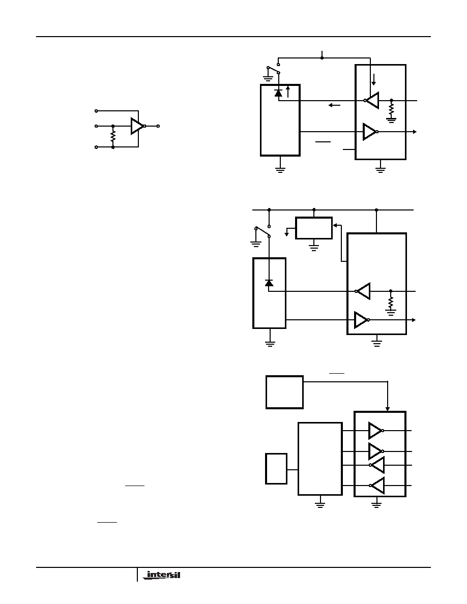
The ISL83384E contains standard inverting receivers that
three-state via the SHDN control line. Receivers driving
powered down peripherals must be disabled to prevent
current flow through the peripheral's protection diodes (see
Figures 2 and 3).
Transmitter Propagation Delay
Transmitter Input to
Transmitter Output,
C
L
= 1000pF
t
PHL
Full
-
0.6
3.5
µ
s
t
PLH
Full
-
0.7
3.5
µ
s
Receiver Propagation Delay
Receiver Input to Receiver
Output, C
L
= 150pF
t
PHL
Full
-
0.2
1
µ
s
t
PLH
Full
-
0.3
1
µ
s
Transmitter Output Enable Time
From SHDN Rising Edge to T
OUT
=
±
3V
25
-
50
-
µ
s
Transmitter Output Disable Time
From SHDN Falling Edge to T
OUT
=
±
5V
25
-
600
-
ns
Transmitter Skew
t
PHL
- t
PLH
(Note 4)
25
-
100
-
ns
Receiver Skew
t
PHL
- t
PLH
25
-
100
-
ns
Transition Region Slew Rate
R
L
= 3k
to 7k
,
Measured From 3V to -3V or
-3V to 3V
V
CC
= 3.3V, C
L
= 150pF to
2500pF
25
4
-
-
V/
µ
s
V
CC
= 4.5V, C
L
= 150pF to
2500pF
25
6
-
-
V/
µ
s
ESD PERFORMANCE
RS-232 Pins (T
OUT
, R
IN
)
Human Body Model
25
-
±
15
-
kV
IEC61000-4-2 Contact Discharge
25
-
±
8
-
kV
IEC61000-4-2 Air Gap Discharge
25
-
±
15
-
kV
All Other Pins
Human Body Model
25
-
±
3
-
kV
NOTE:
4. Transmitter skew is measured at the transmitter zero crossing points.
Electrical Specifications
Test Conditions: V
CC
= 3V to 5.5V, C
1
- C
4
= 0.1
µ
F; Unless Otherwise Specified.
Typicals are at T
A
= 25
o
C (Continued)
PARAMETER
TEST CONDITIONS
TEMP
(
o
C)
MIN
TYP
MAX
UNITS
TABLE 2. POWERDOWN AND ENABLE LOGIC TRUTH TABLE
SHDN
INPUT
TRANSMITTER
OUTPUTS
RECEIVER
OUTPUTS MODE OF OPERATION
H
Active
Active
Normal Operation
L
High-Z
High-Z
Manual Powerdown
ISL83384E
5
All the receivers convert RS-232 signals to CMOS output
levels and accept inputs up to
±
30V while presenting the
required 3k
to 7k
input impedance (see Figure 1) even if
the power is off (V
CC
= 0V). The receivers' Schmitt trigger
input stage uses hysteresis to increase noise immunity and
decrease errors due to slow input signal transitions.
Low Power Operation
This 3V device requires a nominal supply current of 0.3mA,
even at V
CC
= 5.5V, during normal operation (not in
powerdown mode). This is considerably less than the 11mA
current required by comparable 5V RS-232 devices,
allowing users to reduce system power simply by replacing
the old style device with the ISL83384E.
Low Power, Pin Compatible Replacement
Pin compatibility with existing 5V products (e.g., MAX222),
coupled with the wide operating supply range, make the
ISL83384E a potential lower power, higher performance
drop-in replacement for existing 5V applications. As long as
the
±
5V RS-232 output swings are acceptable, and
transmitter pull-up resistors aren't required, the ISL83384E
should work in most 5V applications.
When replacing a device in an existing 5V application, it is
acceptable to terminate C
3
to V
CC
as shown on the "Typical
Operating Circuit". Nevertheless, terminate C
3
to GND if
possible, as slightly better performance results from this
configuration.
Powerdown Functionality
The already low current requirement drops significantly
when the device enters powerdown mode. In powerdown,
supply current drops to 1
µ
A, because the on-chip charge
pump turns off (V+ collapses to V
CC
, V- collapses to GND),
and the transmitter and receiver outputs three-state. This
micro-power mode makes these devices ideal for battery
powered and portable applications.
Software Controlled (Manual) Powerdown
The ISL83384E may be forced into its low power, standby
state via a simple shutdown (SHDN) pin (see Figure 4).
Driving this pin high enables normal operation, while driving
it low forces the IC into it's powerdown state. The time
required to exit powerdown, and resume transmission is less
than 50
µ
s. Connect SHDN to V
CC
if the powerdown function
isn't needed.
R
XOUT
GND
V
ROUT
V
CC
5k
R
XIN
-25V
V
RIN
+25V
GND
V
CC
FIGURE 1. INVERTING RECEIVER CONNECTIONS
FIGURE 2. POWER DRAIN THROUGH POWERED DOWN
PERIPHERAL
OLD
V
CC
POWERED
GND
SHDN = GND
V
CC
Rx
Tx
V
CC
CURRENT
V
OUT
=
V
CC
FLOW
RS-232 CHIP
DOWN
UART
FIGURE 3. DISABLED RECEIVERS PREVENT POWER DRAIN
ISL83384E
TRANSITION
DETECTOR
R
X
T
X
V
CC
V
CC
TO
V
OUT
=
HI-Z
WAKE-UP
LOGIC
POWERED
DOWN
UART
V-
FIGURE 4. CONNECTIONS FOR MANUAL POWERDOWN
PWR
SHDN
CPU
I/O
ISL83384E
MGT
LOGIC
UART
ISL83384E