 | –≠–ª–µ–∫—Ç—Ä–æ–Ω–Ω—ã–π –∫–æ–º–ø–æ–Ω–µ–Ω—Ç: ISL837030 | –°–∫–∞—á–∞—Ç—å:  PDF PDF  ZIP ZIP |

1
Modem Reference
Designs
The ISL837030 and ISL83740 Broadband Wireless Modem
Reference Designs support a wide range of modulation
orders and symbol rates.*
In both Reference Designs, sophisticated coding,
equalization, and symbol recovery techniques are employed,
resulting in robust wireless link performance.
The ISL837030 and ISL83740 Reference Designs support
high-capacity digital microwave radios with data rates up to
238Mbps (ISL83740) and 160Mbps (ISL837030). They
provide a flexible, high performance, economical solution for
fixed wireless applications.
* Differences between the ISL837030 and ISL83740 are marked in text as
needed. Also see
Release Notes on page 25
.
Benefits
∑ Eliminates the need to develop custom ASICs
∑ Optimizes wireless link capacity and Bit Error Rate (BER)
performance
∑ Enables rapid prototyping and compliance testing
∑ Proven technology
∑ Optional Evaluation Kit supports demo requirements,
performance evaluation, and lab testing
Features
∑ Programmable modulation
Both: QPSK, 8PSK, 16QAM, 32QAM
ISL83740 only: 64QAM, 128QAM
∑ Flexible data rates
ISL83740: up to 238Mbps
ISL837030: up to 160Mbps
∑ Programmable symbol rates
∑ Reed Solomon (RS) encoding/decoding
∑ Concatenated coding using RS and PTCM inner code
∑ FCC and ETSI spectral mask compliance
∑ Powerful equalization
Includes
∑ Sample ISL87060MIK Modulator and ISL87060DIK
Demodulator Chip Sets for development and test.
∑ Complete Manufacturing Documentation Package: Bill of
Materials, Schematics, PCBA Fabrication Files, including
Gerber Files.
∑ Test Documentation.
∑ Embedded Monitor and Control Software provides
comprehensive setup and test capabilities. Accepts
commands in binary or ASCII format.
Optional Evaluation Kit
The modem PCBA is mounted on an Evaluation Platform,
allowing the modem to be set up and tested in a standard lab
environment. Includes VHF and L-band IF Interfaces and a
sophisticated Graphical User Interface for Windows
operating systems. (ISL83700EVAL/ISL83740EVAL)
FIGURE 1 Simplified Block Diagram
DAC
LPF
Differential
Baseband
Outputs
Baseband
Loopback
ISL87060DIK
Demodulator/
Decoder
ADC
LPF
Decimating
Matched
Filter
Controller
ASYNC
Serial
Data
Data
Differential
Baseband
Inputs
Level
Offset
FLASH
M
o
de
m
D
i
g
it
a
l
/
P
owe
r
Co
nn
e
c
t
o
r
(
P
2
)
TrimDAC
ISL87060MIK
Modulator/
Encoder
Modem PCBA
May 2002
Datasheet
ISL837030, ISL83740
FN8013.5
Æ
CAUTION: These devices are sensitive to electrostatic discharge; follow proper IC Handling Procedures.
1-888-INTERSIL or 321-724-7143
|
Intersil (and design) is a registered trademark of Intersil Americas Inc.
Copyright © Intersil Americas Inc. 2002. All Rights Reserved
CommLinkTM is a trademark of Intersil Americas Inc.

ISL837030, ISL83740
2
FN8013.5
C
ONTENTS
Functional Description . . . . . . . . . . . . . . . . . . . . . . . . 3
Modulator Functions . . . . . . . . . . . . . . . . . . . . . . 5
1. ISL87060MIK Modulator ASSP . . . . . . . 5
2. Digital to Analog Converter (DAC) . . . . . 5
3. Low Pass Filter (LPF) . . . . . . . . . . . . . . 5
4. Rate Exchange . . . . . . . . . . . . . . . . . . . 5
Demodulator Functions . . . . . . . . . . . . . . . . . . . 5
1. Low Pass Filter (LPF) . . . . . . . . . . . . . . 5
2. ADC . . . . . . . . . . . . . . . . . . . . . . . . . . . . 5
3. FPGA Decimating Filter . . . . . . . . . . . . . 5
4. ISL87060DIK Demodulator ASSP . . . . . 5
5. Baseband Loopback . . . . . . . . . . . . . . . 5
6. Automatic Gain Control (AGC) . . . . . . . . 6
The Controller . . . . . . . . . . . . . . . . . . . . . . . . . . 6
Monitor and Control Software . . . . . . . . . . . . . . 6
Performance Specifications . . . . . . . . . . . . . . . . . . . . 7
Modem Parameters . . . . . . . . . . . . . . . . . . . . . . 7
Modulation, Inner Code Rates, and Ranges . . . 7
Modulator Performance Specifications . . . . . . . 8
Modulator Input Requirements . . . . . . . . . . . . . . 8
Modulator Output Electrical Specifications . . . . . 8
Demodulator Input Requirements . . . . . . . . . . . 9
Demodulator Input Electrical Specifications . . . . 9
Demodulator Performance Specifications . . . . 10
BER Performance (Typical) . . . . . . . . . . . . . . . 10
Controller Parameters . . . . . . . . . . . . . . . . . . . 11
Environmental & Physical Specifications . . . . . . . . . 12
Physical Interface Definition . . . . . . . . . . . . . . . . . . . 13
80-Pin Digital/Power Connector . . . . . . . . . . . . 14
Power Supply Signals . . . . . . . . . . . . . . . 15
M&C Port Signals . . . . . . . . . . . . . . . . . . . 15
Modulator Data Interface Signals . . . . . . . 15
Demodulator Data Interface Signals . . . . 16
Miscellaneous Signals . . . . . . . . . . . . . . . 17
Reserved . . . . . . . . . . . . . . . . . . . . . . . . . 17
8-Pin Baseband Connectors . . . . . . . . . . . . . . 18
Data Timing and Packet Definition . . . . . . . . . . . . . . 19
Modulator Data Input Timing . . . . . . . . . . . . . . 19
Modulator Packet Definition . . . . . . . . . . . . . . . 19
Demodulator Data Output Timing . . . . . . . . . . 20
Demodulator RS Data Packet Definition . . . . . 20
AGC Timing . . . . . . . . . . . . . . . . . . . . . . . . . . . 21
Mechanical Drawings . . . . . . . . . . . . . . . . . . . . . . . . 22
Applications . . . . . . . . . . . . . . . . . . . . . . . . . . . . . . . 23
Support
Related Documentation . . . . . . . . . . . . . . . . . . . . . . 25
Release Notes . . . . . . . . . . . . . . . . . . . . . . . . . . . . . 25
Customer Support . . . . . . . . . . . . . . . . . . . . . . . . . . 25
L
IST OF
F
IGURES
1. Simplified Block Diagram . . . . . . . . . . . . . . . . . . . . . . . . . . . . . . 1
2. Functional Block Diagram . . . . . . . . . . . . . . . . . . . . . . . . . . . . . 3
3. Modem Printed Circuit Board Assembly (PCBA) . . . . . . . . . . . . 4
4. Acquisition/Tracking Range at Low Baud Rates . . . . . . . . . . . 10
5. Modem PCBA Connectors . . . . . . . . . . . . . . . . . . . . . . . . . . . . 13
6. Digital/Power Connector Pin Configuration . . . . . . . . . . . . . . . 14
7. Modulator Connector Pin Configuration . . . . . . . . . . . . . . . . . . 18
8. Demodulator Connector Pin Configuration . . . . . . . . . . . . . . . 18
9. Modulator Data Input Timing . . . . . . . . . . . . . . . . . . . . . . . . . . 19
10. Modulator Packet Definition . . . . . . . . . . . . . . . . . . . . . . . . . . 19
11. Demodulator Data Output Timing . . . . . . . . . . . . . . . . . . . . . 20
12. Demodulator Data Packet Definition . . . . . . . . . . . . . . . . . . . 20
13. AGC Timing . . . . . . . . . . . . . . . . . . . . . . . . . . . . . . . . . . . . . . 21
14. Modem PCBA Mechanical Dimensions (Top View) . . . . . . . . 22
15. Modulator Baseband Interface to ISL83740EVAL/ISL83700EVAL
Platform . . . . . . . . . . . . . . . . . . . . . . . . . . . . . . . . . . . . . . . . . . . . 23
16. Unbalanced Demodulator Baseband Interface, Shorter Runs 24
17. Unbalanced Demodulator Baseband Interface, Longer Runs 24
Ordering Information
PART NUMBER
DESCRIPTION
ISL83740REF-CD
ISL83740 Reference Design (QPSK,
8PSK, 16QAM, 32QAM, 64QAM,
128QAM)
ISL837030REF-CD
ISL837030 Reference Design (QPSK,
8PSK, 16QAM, 32QAM)
ISL837030KIT-xxx
Kit versions supply sample chips in
lots of 24 to 120, in 24-unit increments.
Applies to either Reference Design.
ISL83740EVAL
ISL83740 Evaluation Kit (QPSK,
8PSK, 16QAM, 32QAM, 64QAM,
128QAM)
ISL83700EVAL
ISL837030 Evaluation Kit (QPSK,
8PSK, 16QAM, 32QAM)
ISL87060MIK
Modulator Chip
ISL87060DIK
Demodulator Chip
All Intersil products are manufactured, assembled and tested utilizing ISO9000 quality systems.
Intersil Corporation's quality certifications can be viewed at www.intersil.com/design/quality
Intersil products are sold by description only. Intersil Corporation reserves the right to make changes in circuit design, software and/or specifications at any time without
notice. Accordingly, the reader is cautioned to verify that data sheets are current before placing orders. Information furnished by Intersil is believed to be accurate and
reliable. However, no responsibility is assumed by Intersil or its subsidiaries for its use; nor for any infringements of patents or other rights of third parties which may result
from its use. No license is granted by implication or otherwise under any patent or patent rights of Intersil or its subsidiaries.
For information regarding Intersil Corporation and its products, see www.intersil.com
Sales Office Headquarters
NORTH AMERICA
Intersil Corporation
7585 Irvine Center Drive
Suite 100
Irvine, CA 92618
TEL: (949) 341-7000
FAX: (949) 341-7123
Intersil Corporation
2401 Palm Bay Rd.
Palm Bay, FL 32905
TEL: (321) 724-7000
FAX: (321) 724-7946
EUROPE
Intersil Europe Sarl
Ave. William Graisse, 3
1006 Lausanne
Switzerland
TEL: +41 21 6140560
FAX: +41 21 6140579
ASIA
Intersil Corporation
Unit 1804 18/F Guangdong Water Building
83 Austin Road
TST, Kowloon Hong Kong
TEL: +852 2723 6339
FAX: +852 2730 1433
ISL837030, ISL83740
3
FN8013.5
.
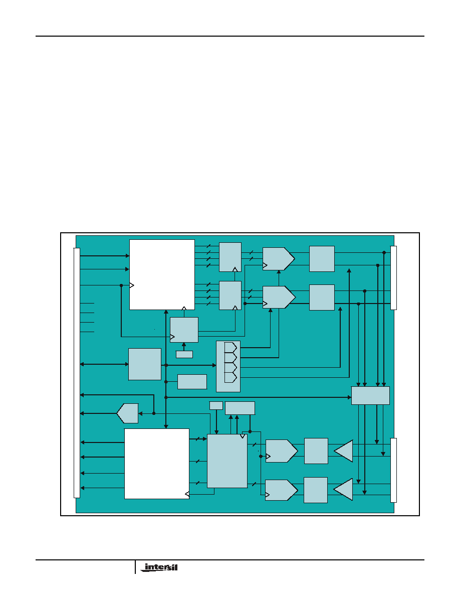
FIGURE 2 Functional Block Diagram
D
e
m
odulat
or
B
a
seba
nd
C
o
n
n
e
c
t
o
r
M
o
d
u
l
a
t
o
r
B
a
s
e
b
a
n
d
C
o
n
n
e
c
t
o
r
D
i
g
i
t
a
l
/
P
o
w
e
r
C
o
n
n
e
c
t
o
r
Data Input
Byte Clock
ISL87060MIK
Modulator/
Encoder
Controller
FLASH
512k X 16
AGC
DAC
VCO
ASYNC Serial
Digital AGC
Analog AGC
Data Output
Data Clock
I Data
10
Q Data
10
Sample Clock
AGC
10
I Data
10
Q Data
10
2-1
Mux
2-1
Mux
10
10 200 Msps
DAC
200 Msps
DAC
Passive
LPF
Passive
LPF
Q Level/Bal
I Level/Bal
Q Offset
I Offset
XO
Clock PLL
FPGA
Decimating
Matched
Filter
Baseband
Loopback
100 Msps
ADC
100 Msps
ADC
Passive
LPF
Passive
LPF
TrimDAC
8
8
Rate
Exchange
FPGA
+3.3V
+5V
+12V
-12V
External Sync
Packet Sync
Data Flag
ISL87060DIK
Demodulator/
Decoder
Modem PCBA
Functional Description
Intersil's broadband wireless modem devices are fully
integrated and support a wide range of modulation
orders and symbol rates. Sophisticated coding,
equalization, and symbol recovery techniques are
employed to enable robust wireless link performance.
The complete modem Printed Circuit Board Assemblies
(PCBAs) with standard hardware and software
interfaces enable equipment manufacturers to rapidly
integrate Intersil modem functionality into their system
products.
The ISL837030 and ISL83740 Modem Reference
Designs provide a flexible, high performance,
economical solution for fixed wireless applications. The
modem design provides an off-the-shelf solution for
users interested in easily integrating a complete modem
into their products.
The modem PCBA architecture implements a complete
baseband transmit and receive function:
1. Modulator Function
Converts byte-wide parallel data, encodes and digitizes
it, and generates a differential baseband analog signal.
This signal can then be up-converted to any IF/RF
frequency the user requires.
2. Demodulator Function
Accepts a differential analog baseband signal. Filters,
decodes, corrects, and converts it to byte-wide digital
data and clock.
3. Controller
Incorporates everything necessary to control and monitor
the modem.
F u n c t i o n a l D e s c r i p t i o n
ISL837030, ISL83740
4
FN8013.5
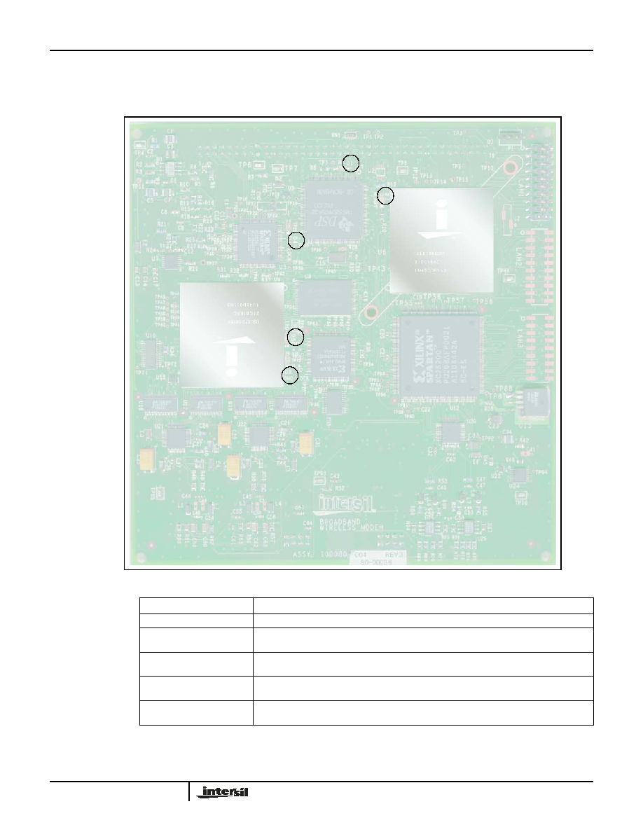
FIGURE 3 Modem Printed Circuit Board Assembly (PCBA)
FPGA
Decimating
Matched
Filter
ISL87060MIK
Modulator
ISL87060DIK
Demodulator
ADC
DAC
DAC
Trim
D6
D5
FPGA
Rate
Exchange
D4
FLASH
Memory
Controller
D1
D3
DAC
MUX
MUX
MUX
MUX
LED INDICATORS
LIGHT INDICATORS
D1 Controller Status
Blinking indicates controller is functional. Solid off or on indicates not functional.
D3 Modem Ready
Light on indicates modem is ready to accept user commands. Equivalent to the
MODEM_RDY
signal on the interface connector.
D4 PLL Lock Detect
Light on indicates that the modulator rate exchange has successfully locked to
the interface input byte clock.
D5 Alarm IRQ
Light on signals active alarm condition. Equivalent to the
IRQ
signal on the
interface connector.
D6 Demod Lock
Light on indicates that the demodulator has successfully locked to the input
baseband signal.

F u n c t i o n a l D e s c r i p t i o n
ISL837030, ISL83740
5
FN8013.5
Modulator Functions
The modulator accepts byte-wide parallel data, encodes it,
digitizes it, and produces a balanced analog signal output.
This signal can then be up-converted to whatever RF/IF
frequency the application requires. It consists of four
functions:
1. ISL87060MIK Modulator ASSP
The modulator ASSP provides a digital representation of a
modulated analog signal. The chip accepts byte-wide TTL
data and applies:
∑ Energy Dispersal
∑ Reed-Solomon Forward Error Correction (FEC)
∑ Convolutional Interleaving
∑ Symbol Generation for various modulation formats with
or without Convolutional Coding
∑ Pulse Shaping
∑ Tuning
The digital output from the ASSP consists of eight 10-bit
ports, four for I and four for Q. Each port represents at least
one of four samples per symbol which requires multiplexing
before it is applied to the Digital to Analog Converter (DAC).
2. Digital to Analog Converter (DAC)
The DAC section muxes each of the four 10-bit ports and
converts them into an analog signal representation of the
digital values produced by the ASSP. The DAC samples at a
minimum of four samples per symbol based on the ASSP's
Interpolator setting.
TrimDACs, controlled by the processor, provide fine
adjustment of the amplitude and DC offset of the I and Q
output signals. Two of the TrimDACs control the reference
voltage used by the output DACs, thereby adjusting the
output signal amplitude. The default setting corresponds to a
zero adjustment.
3. Low Pass Filter (LPF)
The analog signal from the DAC is then filtered to eliminate
undesired digitizing effects. The TrimDAC is used to control
the offset voltage of the output signal, allowing the user to
adjust the balance between the I and Q baseband output
signals for upconverter optimization.
4. Rate Exchange
The Rate Exchange function generates clocks by converting
the byte-wide interface clock to an ASSP processing clock. It
then provides the sample clocks to the DAC and Mux
sections. The relationship between the byte clock input and
the other clocks varies dramatically depending on the FEC
and Interpolator settings within the ASSP.
Demodulator Functions
The demodulator accepts differential analog baseband I and
Q signals, then filters, decodes, corrects, and converts them
to byte-wide digital data and clock. It consists of six functions:
1. Low Pass Filter (LPF)
The LPF eliminates any undesired baseband high frequency
artifacts caused by the down conversion process.
2. ADC
The Analog to Digital Converter (ADC) provides a digital
representation of the modulated baseband analog signal. It
provides eight bits of data for each of the I and Q channels.
3. FPGA Decimating Filter
A Field Programmable Gate Array (FPGA) based Decimating
Matched Filter is provided for additional filtering based on the
desired symbol rate. Multiple FPGA designs are required to
cover the full symbol range. They are stored in the
processor's FLASH memory and loaded as required, based
on configuration parameters. The modem automatically
toggles between the FPGA designs depending on the baud
rate.
4. ISL87060DIK Demodulator ASSP
The demodulator ASSP accepts quantized baseband I and Q
signals and provides all necessary demodulation functions
including:
∑ Carrier and Symbol Acquisition and Tracking
∑ Adaptive Equalization
∑ Data Estimation
∑ Convolutional Deinterleaving
∑ Energy Dispersal Removal
∑ Decoding Functions, including Reed-Solomon
decoding
5. Baseband Loopback
The modulator baseband output can be configured to be
connected to the input of the demodulator. This allows in-
system functional verification of the modem. The loop-back
circuit is implemented with a fully differential buffered/switch
circuit. When engaged, the loop-back signals are summed
with the normal I and Q input signals to the demodulator. This
configuration does not require that either the normal
modulator I/Q outputs or the normal demodulator I/Q inputs
be disconnected. Operation is transparent to the normal
loading on these interfaces.
The loop-back signals are summed with the
normal input signals. Therefore, when loopback
is enabled the system must be set to minimize
the signal input from the normal demodulator I/Q
input path.