
3/20/98
GA150TD120U
"HALF-BRIDGE" IGBT DOUBLE INT-A-PAK
Features
V
CES
=
1200
V
V
CE
(on) typ.
= 2.4V
@V
GE
=
15V
,
I
C
=
150A
Parameter
Typ.
Max.
Units
R
JC
Thermal Resistance, Junction-to-Case - IGBT
--
0.16
R
JC
Thermal Resistance, Junction-to-Case - Diode
--
0.20
∞C/W
R
CS
Thermal Resistance, Case-to-Sink - Module
0.1
--
Mounting Torque, Case-to-Heatsink
--
4.0
N m
Mounting Torque, Case-to-Terminal 1, 2 & 3
--
3.0
Weight of Module
400
--
g
Thermal / Mechanical Characteristics
Absolute Maximum Ratings
Parameter
Max.
Units
V
CES
Collector-to-Emitter Voltage
1200
V
I
C
@ T
C
= 25∞C
Continuous Collector Current
150
I
CM
Pulsed Collector Current
300
A
I
LM
Peak Switching Current
300
I
FM
Peak Diode Forward Current
300
V
GE
Gate-to-Emitter Voltage
±20
V
V
ISOL
RMS Isolation Voltage, Any Terminal To Case, t = 1 min
2500
P
D
@ T
C
= 25∞C
Maximum Power Dissipation
780
W
P
D
@ T
C
= 85∞C
Maximum Power Dissipation
406
T
J
Operating Junction Temperature Range
-40 to +150
∞C
T
STG
Storage Temperature Range
-40 to +125
∑ Standard: Optimized for minimum saturation
voltage and operating frequencies up to 10kHz
∑ Very low conduction and switching losses
∑ HEXFRED
TM
antiparallel diodes with ultra- soft
recovery
∑ Industry standard package
∑ UL approved
Benefits
∑ Increased operating efficiency
∑ Direct mounting to heatsink
∑ Performance optimized for power conversion: UPS,
SMPS, Welding
∑ Lower EMI, requires less snubbing
PRELIMINARY
∑ Generation 4 IGBT technology
.
www.irf.com
1
Ultra-Fast
TM
Speed IGBT
PD - 5.067A

GA150TD120U
2
www.irf.com
Parameter
Min. Typ. Max. Units
Conditions
Q
g
Total Gate Charge (turn-on)
--
1139 1709
V
CC
= 400V, V
GE
= 15V
Q
ge
Gate - Emitter Charge (turn-on)
--
192
288
nC
I
C
= 171A
Q
gc
Gate - Collector Charge (turn-on)
--
377
566
T
J
= 25∞C
t
d(on)
Turn-On Delay Time
--
414
--
R
G1
= 15
, R
G2
= 0
t
r
Rise Time
--
208
--
ns
I
C
= 150A
t
d(off)
Turn-Off Delay Time
--
552
--
V
CC =
720V
t
f
Fall Time
--
342
--
V
GE
= ±15V
E
on
Turn-On Switching Energy
--
29
--
mJ
See Fig.17 through Fig.21
E
off
Turn-Off Switching Energy
--
32
--
E
ts
Total Switching Energy
--
61
90
C
ies
Input Capacitance
--
25630
--
V
GE
= 0V
C
oes
Output Capacitance
--
1139
--
pF
V
CC
= 30V
C
res
Reverse Transfer Capacitance
--
221
--
= 1 MHz
t
rr
Diode Reverse Recovery Time
--
186
--
ns
I
C
= 150A
I
rr
Diode Peak ReverseCurrent
--
133
--
A
R
G1
= 15
Q
rr
Diode Recovery Charge
--
12381 --
nC
R
G2
= 0
di
(rec)
M
/dt
Diode Peak Rate of Fall of Recovery
--
2524
--
A/µs
V
CC =
720V
During t
b
di/dt=1260A/µs
Parameter
Min. Typ. Max. Units
Conditions
V
(BR)CES
Collector-to-Emitter Breakdown Voltage 1200
--
--
V
GE
= 0V, I
C
= 1mA
V
CE(on)
Collector-to-Emitter Voltage
--
2.4
2.9
V
GE
= 15V, I
C
= 150A
--
2.2
--
V
V
GE
= 15V, I
C
= 150A, T
J
= 125∞C
V
GE(th)
Gate Threshold Voltage
3.0
--
6.0
I
C
= 1.75 mA
V
GE(th)
/
T
J
Temperature Coeff. of Threshold Voltage --
-11
--
mV/∞C V
CE
= V
GE
, I
C
= 1.75mA
g
fe
Forward Transconductance
--
201
--
S
V
CE
= 25V, I
C
= 150A
I
CES
Collector-to-Emitter Leaking Current
--
--
2
mA
V
GE
= 0V, V
CE
= 1200V
--
--
20
V
GE
= 0V, V
CE
= 1200V, T
J
= 125∞C
V
FM
Diode Forward Voltage - Maximum
--
2.7
3.5
V
I
F
= 150A, V
GE
= 0V
--
2.6
--
I
F
= 150A, V
GE
= 0V, T
J
= 125∞C
I
GES
Gate-to-Emitter Leakage Current
--
--
500
nA
V
GE
= ±20V
Dynamic Characteristics - T
J
= 125∞C (unless otherwise specified)
Electrical Characteristics @ T
J
= 25∞C (unless otherwise specified)
Details of note
through
are on the last page
GA150TD120U
www.irf.com
3
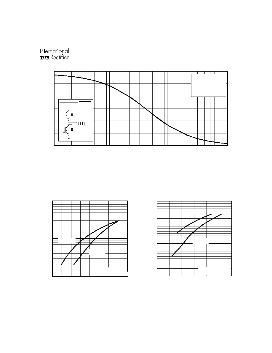
Fig. 1 - Typical Load Current vs. Frequency
(Load Current = I
RMS
of fundamental)
Fig. 2 - Typical Output Characteristics
Fig. 3 - Typical Transfer Characteristics
10
100
1000
1.0
1.5
2.0
2.5
3.0
V , Collector-to-Emitter Voltage (V)
I , Collector-to-Emitter Current (A)
CE
C
V = 15V
80µs PULSE WIDTH
GE
T = 25 C
J
∞
T = 125 C
J
∞
0.1
1
10
100
0
20
40
60
80
100
120
f, Frequency (KHz)
LOAD CURRENT (A)
F or b oth:
D uty c y c le : 50 %
T = 12 5∞ C
T = 90 ∞C
G a te d riv e a s s pe c ified
sink
J
P o w e r D is s ip a tio n = W
6 0 % o f ra te d
v o lta g e
I
Ide a l d io d e s
S q u a re w a v e :
134
Load Current ( A )
1
10
100
1000
5
6
7
8
V , Gate-to-Emitter Voltage (V)
I , Collector-to-Emitter Current (A)
GE
C
V = 50V
5µs PULSE WIDTH
CC
T = 25 C
J
∞
T = 125 C
J
∞
25V

GA150TD120U
4
www.irf.com
Fig. 6 - Maximum Effective Transient Thermal Impedance, Junction-to-Case
Fig. 5 - Typical Collector-to-Emitter Voltage
vs. Junction Temperature
Fig. 4 - Maximum Collector Current vs. Case
Temperature
25
50
75
100
125
150
0
50
100
150
200
T , Case Temperature ( C)
Maximum DC Collector Current(A)
C
∞
-60 -40 -20
0
20
40
60
80 100 120 140 160
1.0
2.0
3.0
4.0
T , Junction Temperature ( C)
V , Collector-to-Emitter Voltage(V)
J
∞
CE
V = 15V
80 us PULSE WIDTH
GE
I = A
300
C
I = A
150
C
I = A
75
C
( ∞C )
0.01
0.1
1
0 . 0 0 0 1
0 . 0 0 1
0 . 0 1
0.1
1
1 0
1 0 0
1 0 0 0
1
th
J
C
D = 0 .5 0
0 .01
0 .0 2
0 .0 5
0 .1 0
0 .2 0
S IN G L E P U L S E
(T H E R M A L R E S P O N S E )
T
h
e
r
m
a
l
R
e
s
p
o
n
s
e
(
Z
)
t , R e cta n g u la r P u ls e D u ra tio n (se c)
A
P
t
2
1
t
DM
Notes:
1. Duty factor D = t / t
2. Peak T = P x Z + T
1
2
J
DM
thJC
C

GA150TD120U
www.irf.com
5
Fig. 7 - Typical Capacitance vs.
Collector-to-Emitter Voltage
Fig. 8 - Typical Gate Charge vs.
Gate-to-Emitter Voltage
Fig. 9 - Typical Switching Losses vs. Gate
Resistance
Fig. 10 - Typical Switching Losses vs.
Junction Temperature
R
G
, Gate Resistance
( )
1
10
100
0
10000
20000
30000
40000
50000
V , Collector-to-Emitter Voltage (V)
C, Capacitance (pF)
CE
V
C
C
C
=
=
=
=
0V,
C
C
C
f = 1MHz
+ C
+ C
C SHORTED
GE
ies
ge
gc ,
ce
res
gc
oes
ce
gc
C
ies
C
oes
C
res
0
200
400
600
800
1000
1200
0
5
10
15
20
Q , Total Gate Charge (nC)
V , Gate-to-Emitter Voltage (V)
G
GE
V
= 400V
I
= 171A
CC
C
0
10
20
30
40
50
50
60
70
80
90
100
R , Gate Resistance (Ohm)
Total Switching Losses (mJ)
G
V = 720V
V = 15V
T = 25 C
I = 150A
CC
GE
J
C
∞
15
-60 -40 -20
0
20
40
60
80 100 120 140 160
10
100
1000
T , Junction Temperature ( C )
Total Switching Losses (mJ)
J
∞
R = 15Ohm
V = 15V
V = 960V
G
GE
CC
I = A
300
C
I = A
150
C
I = A
75
C
R
G1
=15
;R
G2
= 0
125
720V
( )