
Parameter
Max.
Units
V
CES
Collector-to-Emitter Breakdown Voltage
600
V
I
C
@ T
C
= 25∞C
Continuous Collector Current
200
I
C
@ T
C
= 100∞C
Continuous Collector Current
100
A
I
CM
Pulsed Collector Current
400
I
LM
Clamped Inductive Load Current
R
400
V
GE
Gate-to-Emitter Voltage
± 20
V
E
ARV
Reverse Voltage Avalanche Energy
S
160
mJ
V
ISOL
RMS Isolation Voltage, Any Terminal to Case, t=1 min
2500
P
D
@ T
C
= 25∞C
Maximum Power Dissipation
500
P
D
@ T
C
= 100∞C
Maximum Power Dissipation
200
T
J
Operating Junction
-55 to + 150
T
STG
Storage Temperature Range
-55 to + 150
Mounting Torque, 6-32 or M3 Screw
12 lbf ∑in(1.3N∑m)
Parameter
Typ.
Max.
Units
R
JC
Junction-to-Case
≠≠≠
0.25
R
CS
Case-to-Sink, Flat, Greased Surface
0.05
≠≠≠
Wt
Weight of Module
30
≠≠≠
gm
GA200SA60U
PD -50066A
E
C
G
n-channel
Features
∑ UltraFast: Optimized for minimum saturation voltage
and operating frequencies up to 40 kHz in hard
switching, > 200 kHz in resonant mode
∑ Very low conduction and switching losses
∑ Fully isolate package ( 2,500 Volt AC/RMS)
∑ Very low internal inductance (
5 nH typ.)
∑ Industry standard outline
∑ Designed for increased operating efficiency in power
conversion: UPS, SMPS, Welding, Induction heating
∑ Lower overall losses available at frequencies
20kHz
∑ Easy to assemble and parallel
∑ Direct mounting to heatsink
∑ Lower EMI, requires less snubbing
∑ Plug-in compatible with other SOT-227 packages
Benefits
V
CES
= 600V
V
CE(on) typ.
= 1.60V
@V
GE
= 15V, I
C
= 100A
Thermal Resistance
Absolute Maximum Ratings
W
4/24/2000
∞C
V
∞C/W
S O T -2 2 7
INSULATED GATE BIPOLAR TRANSISTOR
Ultra-Fast
TM
Speed IGBT
www.irf.com
1

GA200SA60U
2
www.irf.com
Parameter
Min. Typ. Max. Units
Conditions
V
(BR)CES
Collector-to-Emitter Breakdown Voltage
600
--
--
V
V
GE
= 0V, I
C
= 250µA
V
(BR)ECS
Emitter-to-Collector Breakdown Voltage
T 18
--
--
V
V
GE
= 0V, I
C
= 1.0A
DV
(BR)CES
/DT
J
Temperature Coeff. of Breakdown Voltage
--
0.38
--
V/∞C
V
GE
= 0V, I
C
= 10 mA
--
1.60
1.9
I
C
= 100A V
GE
= 15V
V
CE(ON)
Collector-to-Emitter Saturation Voltage
--
1.92
--
I
C
= 200A
See Fig.2, 5
--
1.54
--
I
C
= 100A , T
J
= 150∞C
V
GE(th)
Gate Threshold Voltage
3.0
--
6.0
V
CE
= V
GE
, I
C
= 250µA
V
GE(th)
/
T
J
Temperature Coeff. of Threshold Voltage
--
-11
--
mV/∞C V
CE
= V
GE
, I
C
= 2.0 mA
g
fe
Forward Transconductance
U
79
--
S
V
CE
= 100V, I
C
= 100A
--
--
1.0
V
GE
= 0V, V
CE
= 600V
--
--
10
V
GE
= 0V, V
CE
= 600V, T
J
= 150∞C
I
GES
Gate-to-Emitter Leakage Current
--
--
±250
nA
V
GE
= ±20V
Parameter
Min. Typ. Max. Units
Conditions
Q
g
Total Gate Charge (turn-on)
--
770 1200
I
C
= 100A
Q
ge
Gate - Emitter Charge (turn-on)
--
100
150
nC
V
CC
= 400V
See Fig. 8
Q
gc
Gate - Collector Charge (turn-on)
--
260
380
V
GE
= 15V
t
d(on)
Turn-On Delay Time
--
54
--
t
r
Rise Time
--
79
--
T
J
= 25∞C
t
d(off)
Turn-Off Delay Time
--
130
200
I
C
= 100A, V
CC
= 480V
t
f
Fall Time
--
300
450
V
GE
= 15V, R
G
= 2.0
E
on
Turn-On Switching Loss
--
0.98
--
Energy losses include "tail"
E
off
Turn-Off Switching Loss
--
3.48
--
mJ
See Fig. 9, 10, 14
E
ts
Total Switching Loss
--
4.46
7.6
t
d(on)
Turn-On Delay Time
--
56
--
T
J
= 150∞C,
t
r
Rise Time
--
75
--
I
C
= 100A, V
CC
= 480V
t
d(off)
Turn-Off Delay Time
--
160
--
V
GE
= 15V, R
G
= 2.0
t
f
Fall Time
--
460
--
Energy losses include "tail"
E
ts
Total Switching Loss
--
7.24
--
mJ
See Fig. 10, 11, 14
L
E
Internal Emitter Inductance
--
5.0
--
nH
Measured 5mm from package
C
ies
Input Capacitance
--
16500 --
V
GE
= 0V
C
oes
Output Capacitance
--
1000
--
pF
V
CC
= 30V
See Fig. 7
C
res
Reverse Transfer Capacitance
--
200
--
= 1.0MHz
T
Pulse width
80µs; duty factor 0.1%.
U
Pulse width 5.0µs, single shot.
Notes:
Q
Repetitive rating; V
GE
= 20V, pulse width limited by
max. junction temperature. ( See fig. 13b )
R
V
CC
= 80%(V
CES
), V
GE
= 20V, L = 10µH, R
G
= 2.0
,
(See fig. 13a)
S
Repetitive rating; pulse width limited by maximum
junction temperature.
Electrical Characteristics @ T
J
= 25∞C (unless otherwise specified)
I
CES
Zero Gate Voltage Collector Current
V
mA
Switching Characteristics @ T
J
= 25∞C (unless otherwise specified)
ns
ns
GA200SA60U
www.irf.com
3
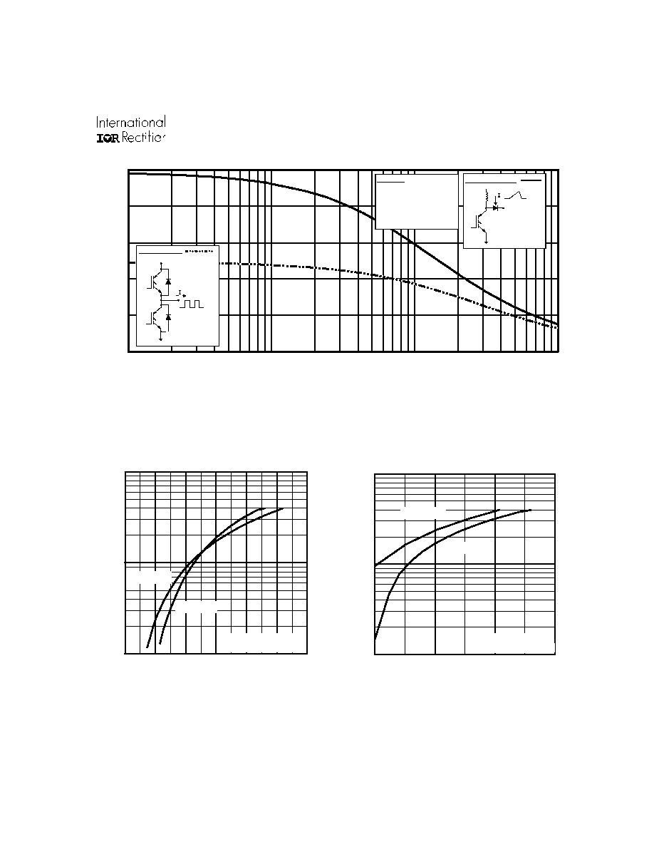
Fig. 1 - Typical Load Current vs. Frequency
(Load Current = I
RMS
of fundamental)
Fig. 2 - Typical Output Characteristics
Fig. 3 - Typical Transfer Characteristics
Load Current ( A )
10
100
1000
0.5
1.0
1.5
2.0
2.5
3.0
3.5
V , Collector-to-Emitter Voltage (V)
I , Collector-to-Emitter Current (A)
CE
C
V = 15V
20µs PULSE WIDTH
GE
T = 25 C
J
∞
T = 150 C
J
∞
10
100
1000
5.0
6.0
7.0
8.0
V , Gate-to-Emitter Voltage (V)
I , Collector-to-Emitter Current (A)
GE
C
V = 25V
20µs PULSE WIDTH
CE
T = 25 C
J
∞
T = 150 C
J
∞
5µs PULSE WIDTH
0
4 0
8 0
1 2 0
1 6 0
2 0 0
0 . 1
1
1 0
1 0 0
f, Fre quen cy (kH z)
A
60% of rated
voltage
Ideal diodes
Square wave:
For both:
Duty cycle: 50%
T = 125∞C
T = 90∞C
Gate drive as specified
sink
J
Triangular wave:
Clamp voltage:
80% of rated
Power Dissipation = 140W

GA200SA60U
4
www.irf.com
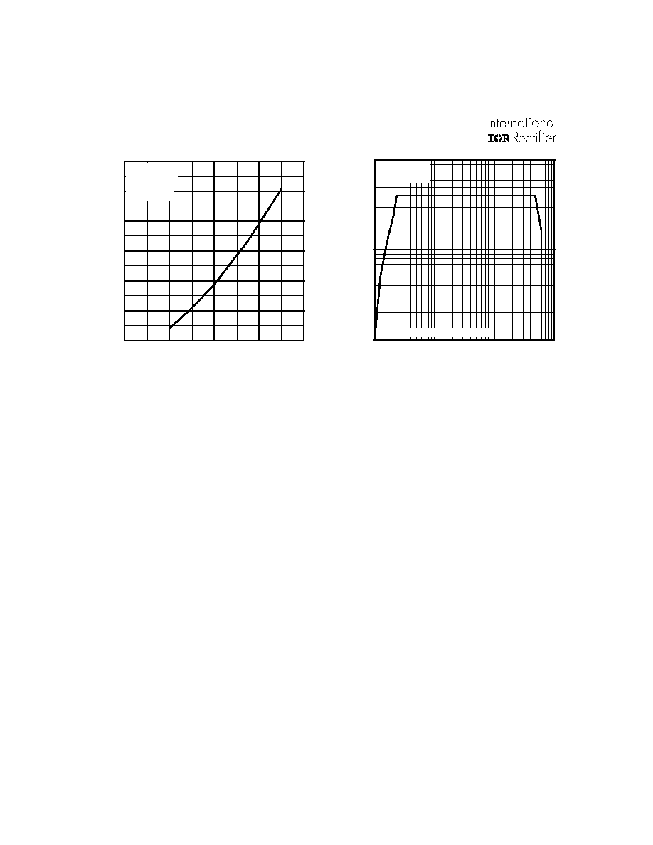
Fig. 6 - Maximum Effective Transient Thermal Impedance, Junction-to-Case
Fig. 5 - Typical Collector-to-Emitter Voltage
vs. Junction Temperature
Fig. 4 - Maximum Collector Current vs. Case
Temperature
-60 -40 -20
0
20
40
60
80 100 120 140 160
1.0
2.0
3.0
T , Junction Temperature ( C)
V , Collector-to-Emitter Voltage(V)
J
∞
CE
V = 15V
80 us PULSE WIDTH
GE
I = A
400
C
I = A
200
C
I = A
100
C
25
50
75
100
125
150
0
50
100
150
200
T , Case Temperature ( C)
Maximum DC Collector Current(A)
C
∞
0.001
0.01
0.1
1
0.00001
0.0001
0.001
0.01
0.1
1
Notes:
1. Duty factor D = t / t
2. Peak T = P
x Z
+ T
1
2
J
DM
thJC
C
P
t
t
DM
1
2
t , Rectangular Pulse Duration (sec)
Thermal Response (Z )
1
thJC
0.01
0.02
0.05
0.10
0.20
D = 0.50
SINGLE PULSE
(THERMAL RESPONSE)

GA200SA60U
www.irf.com
5
-60 -40 -20
0
20
40
60
80 100 120 140 160
1
10
100
T , Junction Temperature ( C )
Total Switching Losses (mJ)
J
∞
R = Ohm
V = 15V
V = 480V
G
GE
CC
I = A
400
C
I = A
200
C
I = A
100
C
0
10
20
30
40
50
60
0
10
20
30
40
50
60
R , Gate Resistance (Ohm)
Total Switching Losses (mJ)
G
V = 480V
V = 15V
T = 25 C
I = 200A
CC
GE
J
C
∞
Fig. 7 - Typical Capacitance vs.
Collector-to-Emitter Voltage
Fig. 8 - Typical Gate Charge vs.
Gate-to-Emitter Voltage
Fig. 9 - Typical Switching Losses vs. Gate
Resistance
Fig. 10 - Typical Switching Losses vs.
Junction Temperature
1
10
100
0
5000
10000
15000
20000
25000
30000
V , Collector-to-Emitter Voltage (V)
C, Capacitance (pF)
CE
V
C
C
C
=
=
=
=
0V,
C
C
C
f = 1MHz
+ C
+ C
C SHORTED
GE
ies
ge
gc ,
ce
res
gc
oes
ce
gc
Cies
Coes
Cres
2.0
I
C
=
350
A
R
G
, Gate Resistance (
)
0
200
400
600
800
0
4
8
12
16
20
Q , Total Gate Charge (nC)
V , Gate-to-Emitter Voltage (V)
G
GE
V
= 400V
I
= 110A
CC
C
GA200SA60U
6
www.irf.com
10
100
1000
1
10
100
1000
V = 20V
T = 125 C
GE
J
o
SAFE OPERATING AREA
V , Collector-to-Emitter Voltage (V)
I , Collector Current (A)
CE
C
0
100
200
300
400
0
10
20
30
40
50
60
I , Collector Current (A)
Total Switching Losses (mJ)
C
R = Ohm
T = 150 C
V = 480V
V = 15V
G
J
CC
GE
∞
Fig. 11 - Typical Switching Losses vs.
Collector Current
Fig. 12 - Turn-Off SOA
2.0
GA200SA60U
www.irf.com
7
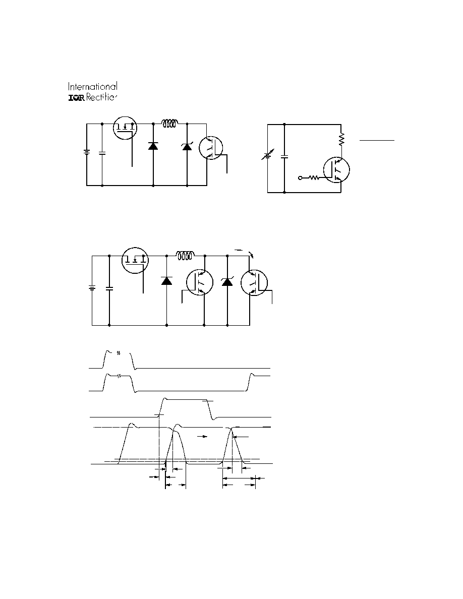
480V
4
X
I
C
@
25∞C
D .U .T.
5 0V
L
V *
C
Q
R
* Driver s am e ty pe as D .U .T .; Vc = 80% o f V ce (m ax )
* No te: D ue to th e 50V p ow er s up p ly, p ulse w id th a nd ind u ctor
w ill inc rea se to o b ta in ra ted Id.
1 00 0V
Fig. 13a -
Clamped Inductive
Load Test Circuit
Fig. 13b -
Pulsed Collector
Current Test Circuit
4 80 µF
9 60 V
0 - 480V
R
L
=
t=5µ s
d (o n )
t
t
f
t
r
90 %
t
d (o ff)
10 %
90 %
1 0%
5 %
V
C
I
C
E
o n
E
o ff
ts o n o ff
E = (E +E )
Q
R
S
Fig. 14b -
Switching Loss
Waveforms
5 0 V
D riv er*
10 00 V
D .U .T.
I
C
C
V
Q
R
S
L
Fig. 14a -
Switching
Loss Test Circuit
* Driver same type
as D.U.T., VC = 480V
GA200SA60U
8
www.irf.com
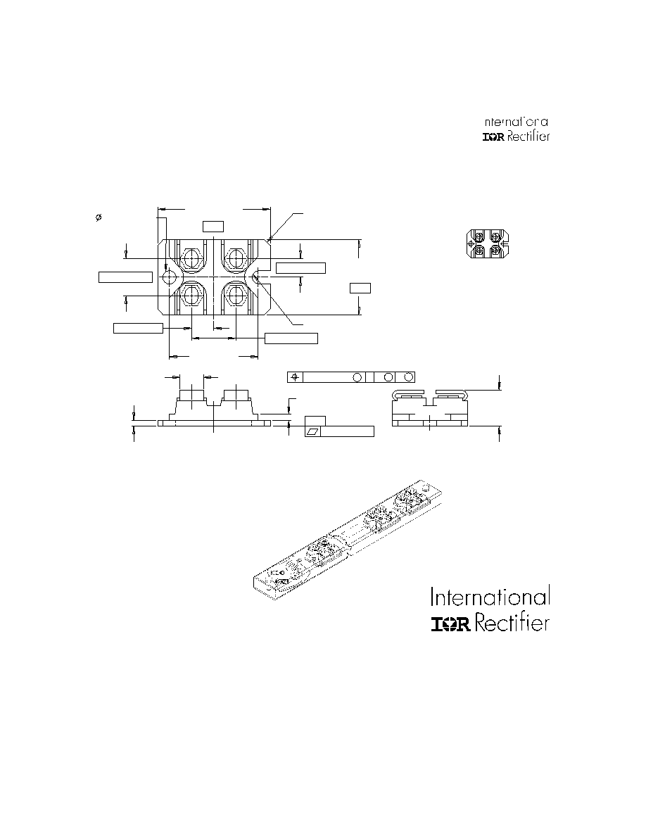
4 .4 0 (.17 3 )
4 .2 0 (.16 5 )
1 2.50 ( .4 92 )
7 .50 ( .2 95 )
2 .1 0 ( .0 82 )
1 .9 0 ( .0 75 )
3 0.2 0 ( 1.1 8 9 )
2 9.8 0 ( 1.1 7 3 )
8 .1 0 ( .31 9 )
7 .7 0 ( .30 3 )
4 X
15 .0 0 ( .59 0 )
R FU L L
2.1 0 ( .0 8 2 )
1.9 0 ( .0 7 5 )
0 .12 ( .0 05 )
-C -
0.2 5 ( .0 10 ) M C A M B M
2 5.7 0 ( 1.01 2 )
2 5.2 0 ( .9 92 )
-B -
6 .25 ( .2 46 )
C H A M FE R
2 .00 ( .0 79 ) X 4 5 7
-A -
38 .3 0 ( 1 .5 0 8 )
37 .8 0 ( 1 .4 8 8 )
12 .3 0 ( .4 84 )
11 .8 0 ( .4 64 )
4
1
3
2
LE A D A S S IG M E N T S
IG B T
E
C
G
E
S
D
G
S
H E X F E T
A 1
K 2
K 1
A 2
3
2
4
1
3
2
4
1
H E X F R E D
E
SOT-227 Package Details
Dimensions are shown in millimeters ( inches )
E
C
IGBT
G
Tube
QUANTITIES PER TUBE IS 10
M4 SREW AND WASHER INCLUDED
IR WORLD HEADQUARTERS: 233 Kansas St., El Segundo, California 90245, USA Tel: (310) 252-7105
IR EUROPEAN REGIONAL CENTRE: 439/445 Godstone Rd, Whyteleafe, Surrey CR3 OBL, UK Tel: ++ 44 (0)20 8645 8000
IR CANADA: 15 Lincoln Court, Brampton, Ontario L6T3Z2, Tel: (905) 453 2200
IR GERMANY: Saalburgstrasse 157, 61350 Bad Homburg Tel: ++ 49 (0) 6172 96590
IR ITALY: Via Liguria 49, 10071 Borgaro, Torino Tel: ++ 39 011 451 0111
IR JAPAN: K&H Bldg., 2F, 30-4 Nishi-Ikebukuro 3-Chome, Toshima-Ku, Tokyo 171 Tel: 81 (0)3 3983 0086
IR SOUTHEAST ASIA: 1 Kim Seng Promenade, Great World City West Tower, 13-11, Singapore 237994 Tel: ++ 65 (0)838 4630
IR TAIWAN:16 Fl. Suite D. 207, Sec. 2, Tun Haw South Road, Taipei, 10673 Tel: 886-(0)2 2377 9936
Data and specifications subject to change without notice. 4/00