Äîêóìåíòàöèÿ è îïèñàíèÿ www.docs.chipfind.ru
Parameter
Typ.
Max.
Units
R
JC
Thermal Resistance, Junction-to-Case - IGBT
--
0.065
R
JC
Thermal Resistance, Junction-to-Case - Diode
--
0.20
°C/W
R
CS
Thermal Resistance, Case-to-Sink - Module
0.04
--
Mounting Torque, Case-to-Heatsink
--
6.0
N m
Mounting Torque, Case-to-Terminal 1, 2
--
5.0
Mounting Torque, Case-to-Terminal 3,4,5,6
--
1.5
Weight of Module
365
--
g
08/27/02
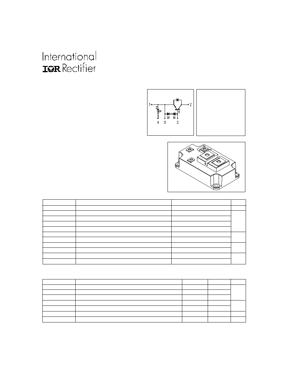
GA600GD25S
SINGLE SWITCH IGBT DUAL INT-A-PAK
Features
V
CES
=
250
V
V
CE
(on) typ.
= 1.25V
@V
GE
=
15V
,
I
C
=
600A
Thermal / Mechanical Characteristics
Standard
TM
Speed IGBT
Absolute Maximum Ratings
Parameter
Max.
Units
V
CES
Collector-to-Emitter Voltage
250
V
I
C
@ T
C
= 25°C
Continuous Collector Current
600
I
CM
Pulsed Collector Current
1200
A
I
LM
Peak Switching Current
1200
I
FM
Peak Diode Forward Current
1200
V
GE
Gate-to-Emitter Voltage
±17
V
V
ISOL
RMS Isolation Voltage, Any Terminal To Case, t = 1 min
2500
P
D
@ T
C
= 25°C
Maximum Power Dissipation
1920
W
P
D
@ T
C
= 85°C
Maximum Power Dissipation
1000
T
J
Operating Junction Temperature Range
-40 to +150
°C
T
STG
Storage Temperature Range
-40 to +125
Benefits
· Increased operating efficiency
· Direct mounting to heatsink
· Performance optimized for power conversion: UPS,
SMPS, Welding
· Lower EMI, requires less snubbing
· Standard speed, optimized for battery powered
application
· Very low conduction losses
· HEXFRED
TM
antiparallel diodes with ultra-soft
recovery
· Industry standard package
· UL recognition pending
· Internal thermistor
.
www.irf.com
1
PD - 50071C
GA600GD25S
2
www.irf.com
Parameter
Min. Typ. Max. Units
Conditions
V
(BR)CES
Collector-to-Emitter Breakdown Voltage
250
--
--
V
GE
= 0V, I
C
= 1mA
V
CE(on)
Collector-to-Emitter Voltage
--
1.25
1.4
V
GE
= 15V, I
C
= 600A
--
1.25
--
V
V
GE
= 15V, I
C
= 600A, T
J
= 125°C
V
GE(th)
Gate Threshold Voltage
3.0
--
6.0
I
C
= 5.0mA, V
CE
= 6.0V
V
GE(th)
/
T
J
Temperature Coeff. of Threshold Voltage
--
-11
--
mV/°C V
CE
= 6.0V, I
C
= 5.0mA,T
C
= 25/125°C
g
fe
Forward Transconductance
--
720
--
S
V
CE
= 25V, I
C
= 600A
I
CES
Collector-to-Emitter Leaking Current
--
--
2.0
mA
V
GE
= 0V, V
CE
= 250V
--
--
20
V
GE
= 0V, V
CE
= 250V, T
J
= 125°C
V
FM
Diode Forward Voltage - Maximum
--
1.5
1.8
V
I
F
= 300A, V
GE
= 0V
--
1.5
--
I
F
= 300A, V
GE
= 0V, T
J
= 125°C
I
GES
Gate-to-Emitter Leakage Current
--
--
1.0
µA
V
GE
= ±14V (18V zeners gate-emitter)
T
DP
Pulse Diode Temp Rise
--
--
80
°C
I
C
= 300A, t = 150msec, Tc =70°C
R-T
25
Thermistor, Positive Temp Coefficient
738
820
902
I
= 100mA,P = 2.5mW/°C (see note 1)
Parameter
Min. Typ. Max. Units
Conditions
Q
g
Total Gate Charge (turn-on)
--
3825 5738
V
CC
= 200V, V
GE
= 15V
Qge
Gate - Emitter Charge (turn-on)
--
555
832
nC
I
C
= 600A
Q
gc
Gate - Collector Charge (turn-on)
--
1262 1893
T
J
= 25°C
t
d(on)
Turn-On Delay Time
--
1060
--
R
G1
= 15
, R
G2
= 0
,
t
r
Rise Time
--
950
--
ns
I
C
= 600A
t
d(off)
Turn-Off Delay Time
--
846
--
V
CC =
150V,
Inductor load
t
f
Fall Time
--
934
--
V
GE
= ±15V
E
on
Turn-On Switching Energy
--
17
--
mJ
See Fig. 17, 19
E
off (1)
Turn-Off Switching Energy
--
105
--
E
ts (1)
Total Switching Energy
--
122
250
C
ies
Input Capacitance
--
86063
--
V
GE
= 0V
C
oes
Output Capacitance
--
9754
--
pF
V
CC
= 30V
C
res
Reverse Transfer Capacitance
--
1913
--
= 1 MHz
t
rr
Diode Reverse Recovery Time
--
314
--
ns
I
C
= 600A
I
rr
Diode Peak ReverseCurrent
--
80
--
A
R
G1
= 15
Q
rr
Diode Recovery Charge
--
12513
--
µC
R
G2
= 0
di
(rec)
M
/dt
Diode Peak Rate of Fall of Recovery
--
632
--
A/µs
V
CC =
150V
During t
b
di/dt = 500A/µs
Dynamic Characteristics - T
J
= 125°C (unless otherwise specified)
Electrical Characteristics @ T
J
= 25°C (unless otherwise specified)
Notes:
1. The thermistor has an average rate of change of 7
/°C between 20°C and 125°C.
Consult U.S. Sensor data sheet for P821GS1K for details
GA600GD25S
www.irf.com
3
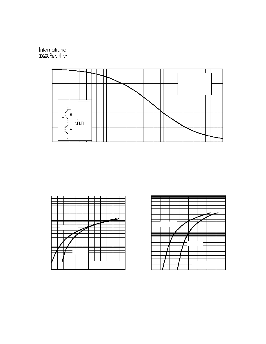
0.1
1
10
100
0
100
200
300
400
500
f, Frequency (KHz)
L
O
AD CURRENT (
A
)
Fig. 1 - Typical Load Current vs. Frequency
(Load Current = I
RMS
of fundamental)
Fig. 2 - Typical Output Characteristics
Fig. 3 - Typical Transfer Characteristics
For both:
Duty cycle: 50%
T = 125°C
T = 90°C
Gate drive as specified
sink
J
Power Dissipation = W
60% of rated
voltage
I
Ideal diodes
Square wave:
333
10
100
1000
10000
0.6
0.8
1.0
1.2
1.4
1.6
1.8
V , Collector-to-Emitter Voltage (V)
I , Col
l
e
ctor Current (A)
CE
C
V = 15V
80µs PULSE WIDTH
GE
T = 25 C
J
°
T = 125 C
J
°
1
10
100
1000
10000
4.0
5.0
6.0
7.0
8.0
V , Gate-to-Emitter Voltage (V)
I , C
o
lle
cto
r-to
-
E
m
itte
r C
u
rre
n
t
(A
)
GE
C
V = 25V
80µs PULSE WIDTH
CE
T = 25 C
J
°
T = 125 C
J
°
GA600GD25S
4
www.irf.com
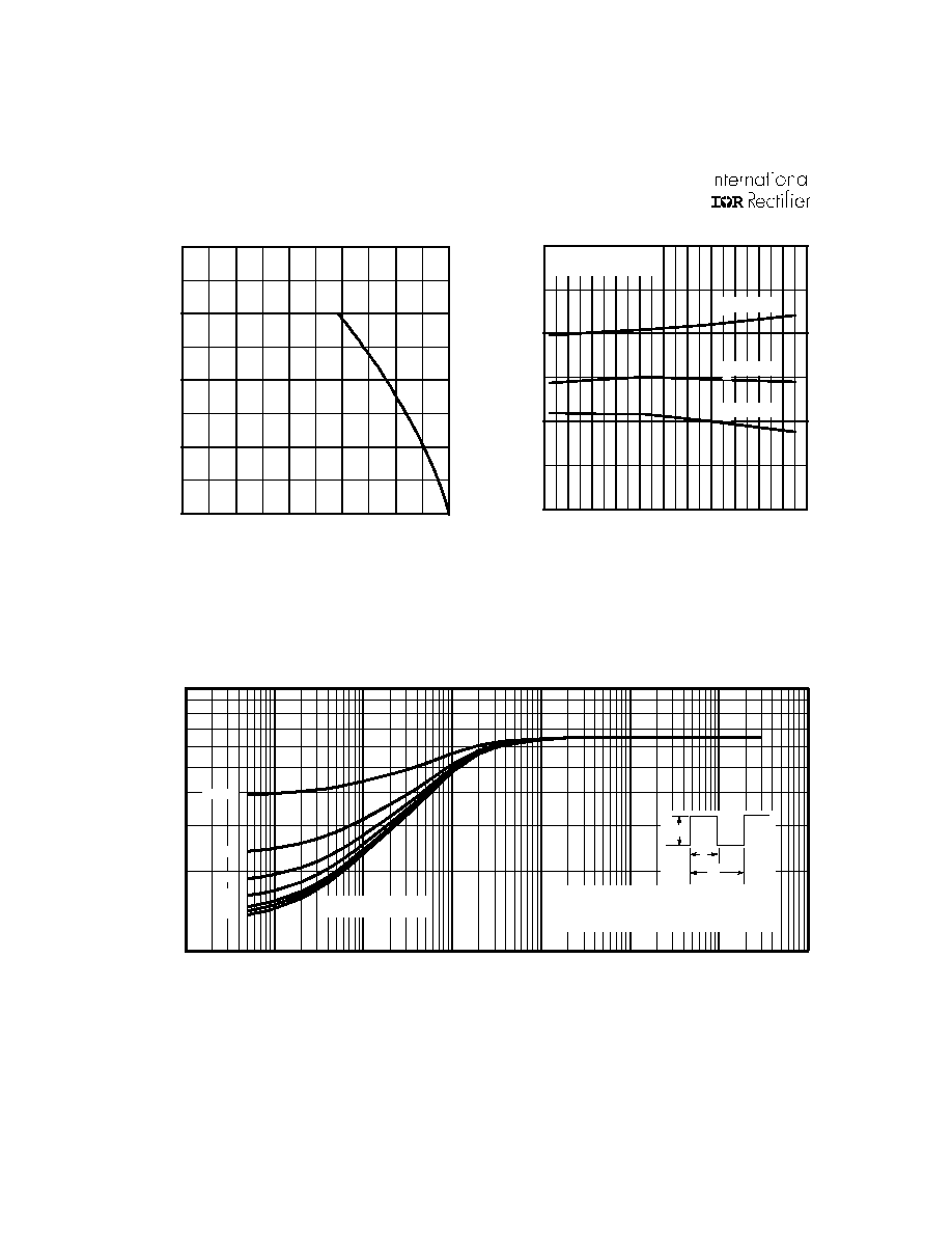
Fig. 6 - Maximum Effective Transient Thermal Impedance, Junction-to-Case
Fig. 5 - Typical Collector-to-Emitter Voltage
vs. Junction Temperature
Fig. 4 - Maximum Collector Current vs. Case
Temperature
0.01
0.1
0.0001
0.001
0.01
0.1
1
10
100
1000
t , Rectangular Pulse Duration (sec)
1
th
J
C
D = 0.50
0.01
0.02
0.05
0.10
0.20
SINGLE PULSE
(THERMAL RESPONSE)
A
T
her
m
a
l
R
e
s
pons
e (
Z
)
P
t
2
1
t
DM
Notes:
1. Duty factor D = t / t
2. Peak T = P x Z + T
1
2
J
DM
thJC
C
-60 -40 -20
0
20
40
60
80 100 120 140 160
0.5
1.0
1.5
2.0
T , Junction Temperature ( C)
V , Col
l
e
ctor-to-Emi
tter Vol
t
age(V)
J
°
CE
V = 15V
80 us PULSE WIDTH
GE
I = A
1200
C
I = A
600
C
I = A
300
C
= 1000A
25
50
75
100
125
150
0
200
400
600
800
T , Case Temperature ( C)
Max
i
mum DC Col
l
e
c
t
or
Cur
r
ent
(
A
)
C
°
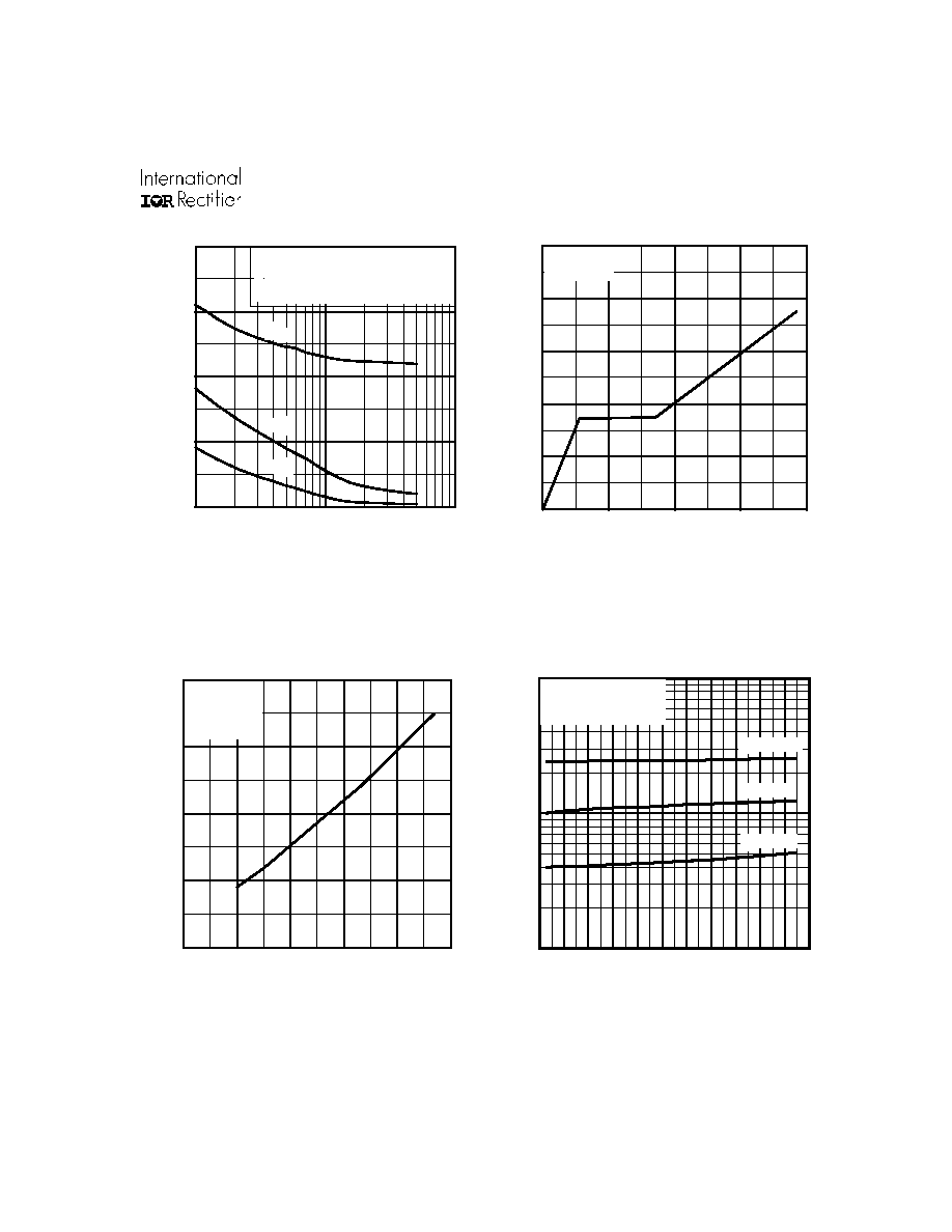
GA600GD25S
www.irf.com
5
250V
Fig. 7 - Typical Capacitance vs.
Collector-to-Emitter Voltage
Fig. 8 - Typical Gate Charge vs.
Gate-to-Emitter Voltage
Fig. 9 - Typical Switching Losses vs. Gate
Resistance
Fig. 10 - Typical Switching Losses vs.
Junction Temperature
0
10
20
30
40
50
110
120
130
140
150
R , Gate Resistance
Tot
a
l
Sw
i
t
chi
ng Losses (
m
J)
G
V = 150V
V = 15V
T = 25 C
I = 600A
CC
GE
J
C
°
( )
0
1000
2000
3000
4000
0
4
8
12
16
20
Q , Total Gate Charge (nC)
V , Gate-to-Emi
t
ter Vol
t
age (V)
G
GE
V
= 400V
I
= 600A
CC
C
1
10
100
0
40000
80000
120000
160000
V , Collector-to-Emitter Voltage (V)
C, Capacitance (pF)
CE
V
C
C
C
=
=
=
=
0V,
C
C
C
f = 1MHz
+ C
+ C
C SHORTED
GE
ies
ge
gc ,
ce
res
gc
oes
ce
gc
C
res
C
oes
C
ies
200V
10
100
1000
-60
-40
-20
0
20
40
60
80
100
120 140
160
T
o
t
a
l
S
w
it
chi
n
g
Los
ses
(
m
J
)
A
T , Junction Temperature (°C)
J
R = 15
; R = 0
V = 15V
V = 150V
I = 1000A
I = 600A
I = 300A
G
GE
CC
G2
C
C
C