Äîêóìåíòàöèÿ è îïèñàíèÿ www.docs.chipfind.ru
Parameter
Max
Units
V
R
Cathode-to-Anode Voltage
600
V
I
F
@ T
C
= 100°C
Continuous Forward Current
8.0
I
FSM
Single Pulse Forward Current
60
I
FRM
Maximum Repetitive Forward Current
24
P
D
@ T
C
= 25°C
Maximum Power Dissipation
36
P
D
@ T
C
= 100°C
Maximum Power Dissipation
14
T
J
Operating Junction and
T
STG
Storage Temperature Range
Ultrafast Recovery
Ultrasoft Recovery
Very Low
I
RRM
Very Low
Q
rr
Specified at Operating Conditions
Lead-Free
Benefits
Reduced RFI and EMI
Reduced Power Loss in Diode and Switching
Transistor
Higher Frequency Operation
Reduced Snubbing
Reduced Parts Count
Features
Description
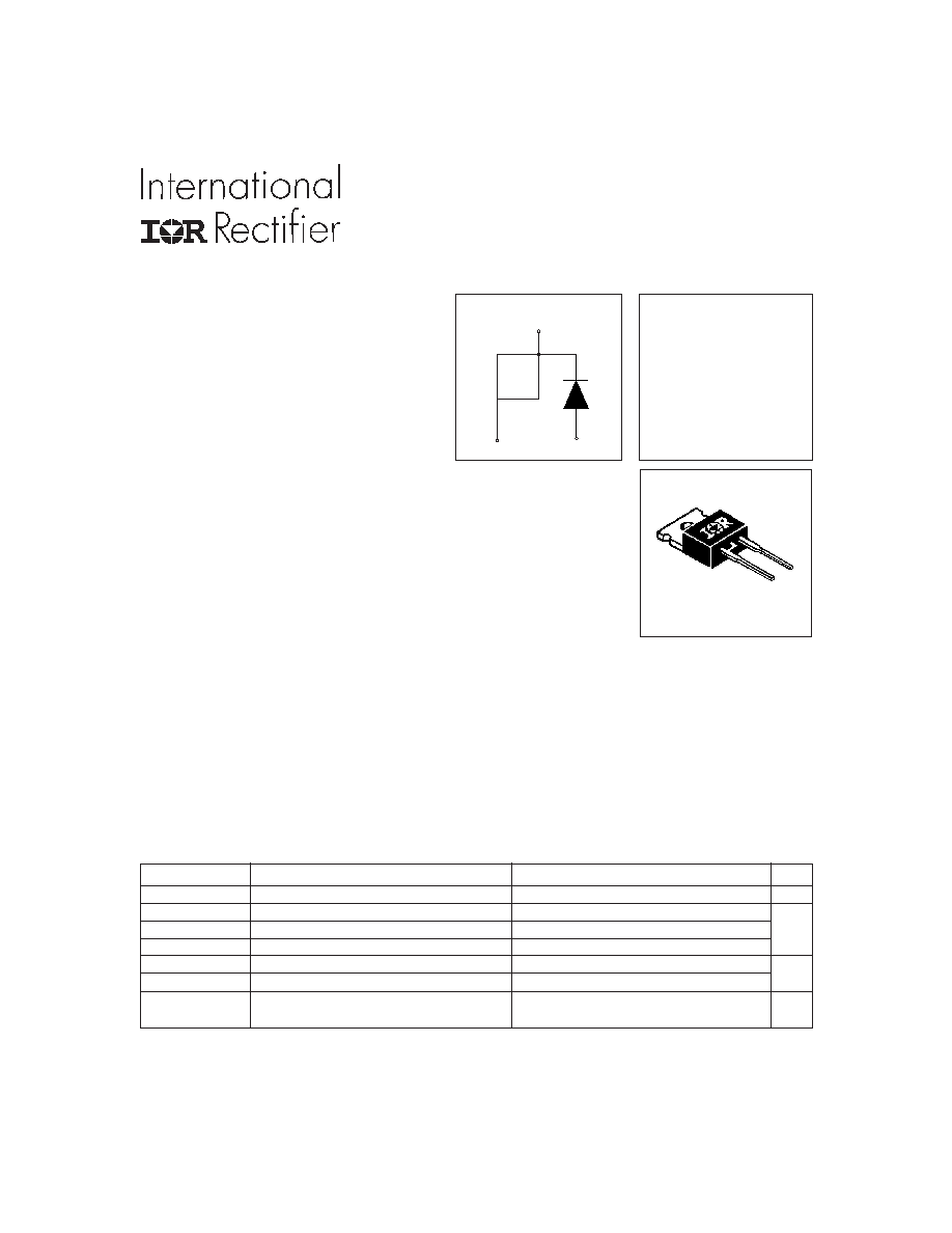
International Rectifier's HFA08TB60 is a state of the art ultra fast recovery
diode. Employing the latest in epitaxial construction and advanced processing
techniques it features a superb combination of characteristics which result in
performance which is unsurpassed by any rectifier previously available. With
basic ratings of 600 volts and 8 amps continuous current, the HFA08TB60 is
especially well suited for use as the companion diode for IGBTs and MOSFETs.
In addition to ultra fast recovery time, the HEXFRED product line features
extremely low values of peak recovery current (I
RRM
) and does not exhibit any
tendency to "snap-off" during the t
b
portion of recovery. The HEXFRED features
combine to offer designers a rectifier with lower noise and significantly lower
switching losses in both the diode and the switching transistor. These HEXFRED
advantages can help to significantly reduce snubbing, component count and
heatsink sizes. The HEXFRED HFA08TB60 is ideally suited for applications in
power supplies and power conversion systems (such as inverters), motor
drives, and many other similar applications where high speed, high efficiency
is needed.
Ultrafast, Soft Recovery Diode
HEXFRED
TM
HFA08TB60PbF
Absolute Maximum Ratings
- 55 to +150
W
A
C
10/18/04
V
R
= 600V
V
F
(typ.)* = 1.4V
I
F(AV)
= 8.0A
Q
rr
(typ.)= 65nC
I
RRM
= 5.0A
t
rr
(typ.)
= 18ns
di
(rec)M
/dt (typ.) = 240A/µs
*
125°C
TO-220AC
1
BASE
CATHODE
2
3
CATHODE
ANODE
2
4
PD-95737
www.irf.com
1
2
www.irf.com
HFA08TB60PbF
Parameter
Min
Typ
Max
Units
T
lead
Lead Temperature
300
°C
R
th
JC
Thermal Resistance, Junction to Case
3.5
R
th
JA
Thermal Resistance, Junction to Ambient
80
R
th
CS
Thermal Resistance, Case to Heat Sink
0.5
2.0
g
0.07
(oz)
6.0
12
Kg-cm
5.0
10
lbfin
Parameter
Min Typ Max Units Test Conditions
t
rr
Reverse Recovery Time
18
I
F
= 1.0A, di
f
/dt = 200A/µs, V
R
= 30V
t
rr1
37
55
ns
T
J
= 25°C
t
rr2
55
90
T
J
= 125°C
I
F
= 8.0A
I
RRM1
Peak Recovery Current
3.5
5.0
T
J
= 25°C
I
RRM2
4.5
8.0
T
J
= 125°C
V
R
= 200V
Q
rr1
Reverse Recovery Charge
65
138
T
J
= 25°C
Q
rr2
124 360
T
J
= 125°C
di
f
/dt = 200A/µs
di
(rec)M
/dt1 Peak Rate of Fall of Recovery Current
240
T
J
= 25°C
di
(rec)M
/dt2 During t
b
210
T
J
= 125°C
Parameter
Min Typ Max Units
Test Conditions
V
BR
Cathode Anode Breakdown Voltage
600
V
I
R
= 100µA
1.4
1.7
I
F
= 8.0A
1.7
2.1
V
I
F
= 16A
1.4
1.7
I
F
= 8.0A, T
J
= 125°C
0.3
5.0
V
R
= V
R
Rated
100 500
T
J
= 125°C, V
R
= 0.8 x V
R
Rated
D
Rated
C
T
Junction Capacitance
10
25
pF
V
R
= 200V
Measured lead to lead 5mm from
package body
Electrical Characteristics @ T
J
= 25°C (unless otherwise specified)
Dynamic Recovery Characteristics @ T
J
= 25°C (unless otherwise specified)
A/µs
nC
A
L
S
Series Inductance
8.0
nH
See Fig. 3
See Fig. 2
See Fig. 1
Thermal - Mechanical Characteristics
See Fig. 5, 6 & 16
See Fig. 7& 8
See Fig. 9 & 10
See Fig. 11 & 12
K/W
V
FM
Max Forward Voltage
µA
Max Reverse Leakage Current
I
RM
Wt
Weight
Mounting Torque
0.063 in. from Case (1.6mm) for 10 sec
Typical Socket Mount
Mounting Surface, Flat, Smooth and Greased
3
www.irf.com
HFA08TB60PbF
0.01
0.1
1
10
0.00001
0.0001
0.001
0.01
0.1
1
Notes:
1. Duty factor D = t / t
2. Peak T = P
x Z
+ T
1
2
J
DM
thJC
C
P
t
t
DM
1
2
t , Rectangular Pulse Duration (sec)
T
herm
a
l
R
e
s
pons
e
(
Z
)
1
th
J
C
0.01
0.02
0.05
0.10
0.20
D = 0.50
SINGLE PULSE
(THERMAL RESPONSE)
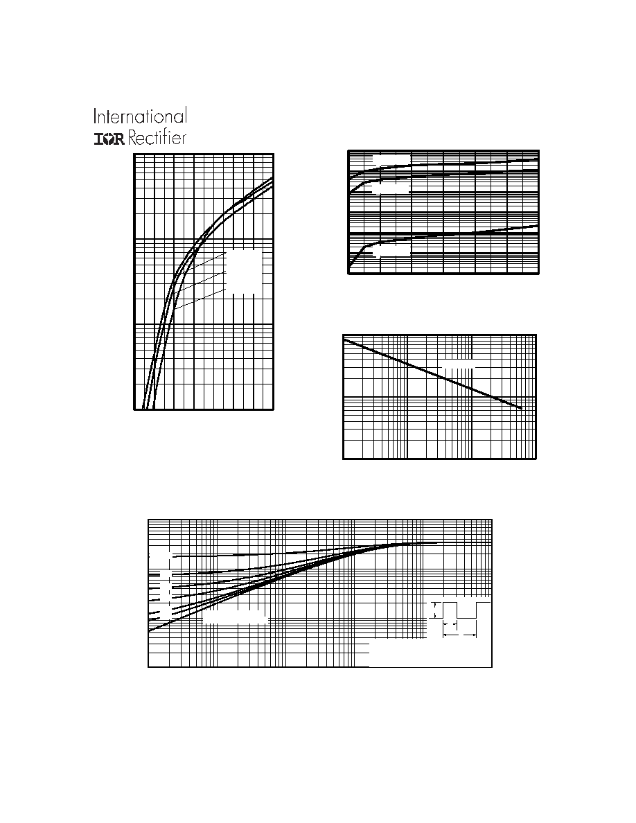
Fig. 4 - Maximum Thermal Impedance Z
thjc
Characteristics
Fig. 2 - Typical Reverse Current vs. Reverse
Voltage
Fig. 3 - Typical Junction Capacitance vs.
Reverse Voltage
Fig. 1 - Maximum Forward Voltage Drop
vs. Instantaneous Forward Current
0.1
1
10
100
0.4
0.8
1.2
1.6
2.0
2.4
2.8
3.2
FM
T = 150°C
T = 125°C
T = 25°C
J
J
J
Forward Voltage Drop - V (V)
0.001
0.01
0.1
1
10
100
1000
0
100
200
300
400
500
600
R
T = 150°C
T = 125°C
T = 25°C
J
J
J
Reverse Voltage - V (V)
1
10
100
1
10
100
1000
T = 25°C
J
Reverse Voltage - V (V)
R
A
Instantaneous
Forward
Current
-
I
F
(A)
Reverse
Current
-
I
R
(µA)
Junction
Capacitance
-C
T
(pF)
4
www.irf.com
HFA08TB60PbF
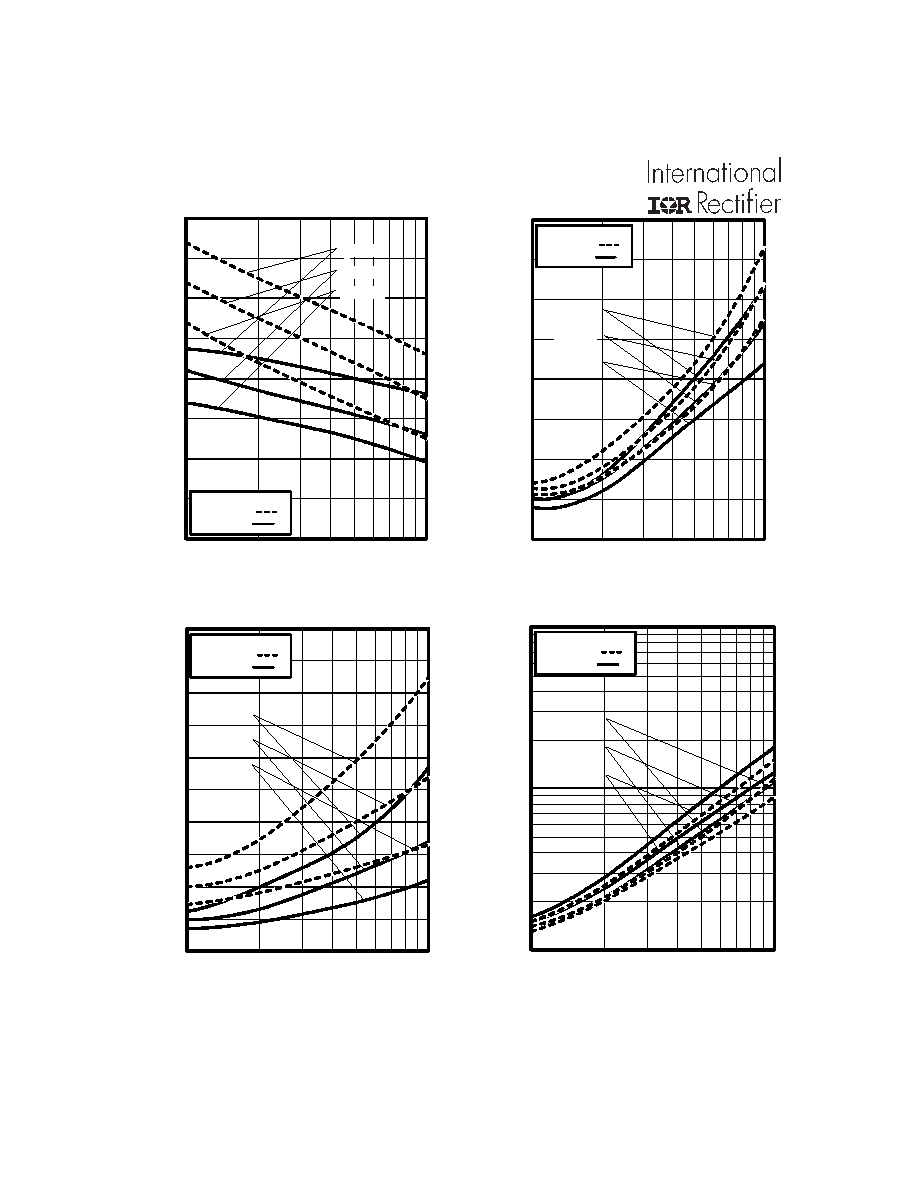
Fig. 7 - Typical Stored Charge vs. di
f
/dt
Fig. 8 - Typical di
(rec)M
/dt vs. di
f
/dt
Fig. 5 - Typical Reverse Recovery vs. di
f
/dt
Fig. 6 - Typical Recovery Current vs. di
f
/dt
0
20
40
60
80
100
1000
f
di /dt - (A/µs)
I = 16A
I = 8.0A
I = 4.0A
V = 200V
T = 125°C
T = 25°C
R
J
J
F
F
F
0
5
10
15
20
100
1000
f
di /dt - (A/µs)
I = 16A
I = 8.0A
I = 4.0A
V = 200V
T = 125°C
T = 25°C
R
J
J
F
F
F
0
100
200
300
400
500
100
1000
f
di /dt - (A/µs)
I = 16A
I = 8.0A
I = 4.0A
V = 200V
T = 125°C
T = 25°C
R
J
J
F
F
F
100
1000
10000
100
1000
f
di /dt - (A/µs)
I = 16A
I = 8.0A
I = 4.0A
V = 200V
T = 125°C
T = 25°C
R
J
J
F
F
F
t
r
r
- (nC)
Irr-
(
A
)
di
(rec)
M/dt-
(
A
/
µ
s
)
Q
r
r
- (nC)
5
www.irf.com
HFA08TB60PbF
4. Q
rr
- Area under curve defined by t
rr
and I
RRM
t
rr
X I
RRM
Q
rr
=
2
5. di
(rec)M
/dt - Peak rate of change of
current during t
b
portion of t
rr
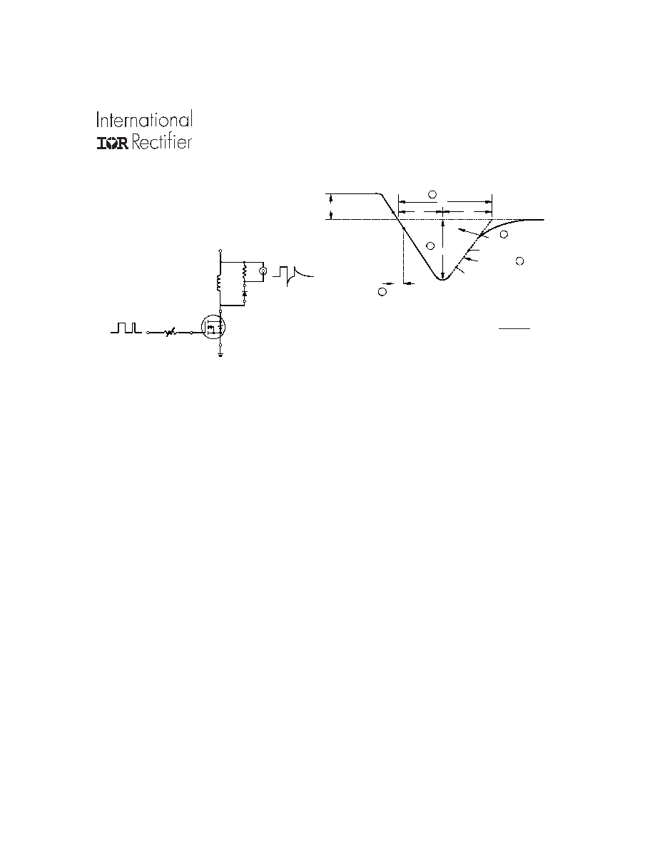
Fig. 10 - Reverse Recovery Waveform and
Definitions
Fig. 9 - Reverse Recovery Parameter Test
Circuit
t
a
t
b
t
rr
Q
rr
I
F
I
RRM
I
RRM
0.5
di(rec)M/dt
0.75 I
RRM
5
4
3
2
0
1
di /dt
f
1. di
f
/dt - Rate of change of current
through zero crossing
2. I
RRM
- Peak reverse recovery current
3. trr - Reverse recovery time measured
from zero crossing point of negative
going I
F
to point where a line passing
through 0.75 I
RRM
and 0.50 I
RRM
extrapolated to zero current
REVERSE RECOVERY CIRCUIT
IRFP250
D.U.T.
L = 70µH
V = 200V
R
0.01
G
D
S
dif/dt
ADJUST
6
www.irf.com
HFA08TB60PbF
Data and specifications subject to change without notice.
IR WORLD HEADQUARTERS: 233 Kansas St., El Segundo, California 90245, USA Tel: (310) 252-7105
TAC Fax: (310) 252-7903
Visit us at www.irf.com for sales contact information. 10/04
TO-220AC Package Outline
Dimensions are shown in millimeters (inches)
TO-220AC Part Marking Information
PART NUMBER
P = LEAD-F RE E
YEAR 1 = 2001
DAT E CODE
LOT CODE
ASS EMBLY
RECT IFIE R
INT ERNAT IONAL
EXAMPLE:
AS SE MBLE D ON WW 19, 2001
IN T HE ASS EMBLY LINE "C"
T HIS IS A HFA06T B120
LOT CODE 1789
LOGO
P = LE AD-F RE E
PART NUMB ER
WEE K 19
YEAR 1 = 2001
DAT E CODE
INT ERNAT IONAL
RE CT IF IER
ASS EMB LY
LOT CODE
E XAMPLE :
IN THE AS SEMBLY LINE "C"
ASS EMBLED ON WW 19, 2001
LOT CODE 1789
T HIS IS A HF A06T B120
LOGO
WEE K 19
LINE C