IR05H40CSP prel revA.PMD
Preliminary Data Sheet I0170J rev. A 06/05
1
Description
International Rectifier's FlipKY product family utilizes wafer level chip scale packaging to deliver Schottky diodes with
the lowest V
F
to PCB footprint area in industry. The three pad 0.9mm x 1.2mm devices can deliver up to 0.5A and
occupy only 1.08mm
2
of board space. The anode and cathode connections are made through solder bump pads on
one side of the silicon rather than through protruding leads enabling designers to strategically place the diodes on the
PCB. This design not only minimizes board space but also reduces thermal resistance and inductance, which can
improve overall circuit efficiency.
Typical applications include hand-held, portable equipment such as cell phones, MP3 players, PDAs, and portable hard
disk drives where space savings and performance are crucial.
Features
·
Ultra Low V
F
To Footprint Area
·
Very Low Profile (<0.6mm)
·
Low Thermal Resistance
·
Supplied Tested And On Tape & Reel
Applications
·
Reverse Polarity Protection
·
Current Steering
·
Freewheeling
·
Flyback
·
Oring
FlipKY
TM
FlipKY
TM
0.5 Amp
40 Volt
IR05H40CSP
Major Ratings and Characteristics
I
F(AV)
Rectangular waveform
0.5
A
V
RRM
40
V
I
FSM
@ tp = 5 µs sine
190
A
V
F
@
0.5 Apk, T
J
=125°C
0.42
V
T
J
range
- 55 to 150
°C
Characteristics
IR05H40CSP
Units
IR05H40CSP
Preliminary Data Sheet I0170J rev. A 06/05
2
T
J
Max. Junction Temperature Range (*)
- 55 to 150
°C
T
stg
Max. Storage Temperature Range
- 55 to 150
°C
R
thJLB
Typ. Thermal Resistance Junction
35
°C/W DC operation
to PCB
(**)
R
thJA
Max. Thermal Resistance Junction
150
°C/W
to Ambient (**)
V
R
Max. DC Reverse Voltage (V)
V
RWM
Max. Working Peak Reverse Voltage (V)
40
Voltage Ratings
I
F(AV)
Max. Average Forward Current
0.5
A
50% duty cycle @ T
PCB
= 114 °C, rectangular wave form
I
FSM
Max. Peak One Cycle Non-Repetitive
190
A
5µs Sine or 3µs Rect. pulse
Surge Current @ 25°C
10
10ms Sine or 6ms Rect. pulse
E
AS
Non- Repetitive Avalanche Energy
5
mJ
T
J
= 25 °C, I
AS
= 2.0A, L = 5.0mH
I
AR
Repetitive Avalanche Current
0.5
A
Current decaying linearly to zero in 1 µsec
Frequency limited by T
J
max. Va = 1.5 x Vr typical
Parameters
Value Units
Conditions
Absolute Maximum Ratings
Following any rated
load condition and
with rated V
RRM
applied
Part number
IR05H40CSP
Thermal-Mechanical Specifications
Parameters
Value
Units
Conditions
<
thermal runaway condition for a diode on its own heatsink
(*) dPtot
1
dTj
Rth( j-a)
(1) Pulse Width < 300µs, Duty Cycle < 2%
V
FM
Max. Forward Voltage (1)
0.48
0.52
V
@ 0.5A
T
J
= 25 °C
Drop
0.54
0.58
@ 1A
* See Fig. 1
0.38
0.42
@ 0.5A
T
J
= 125 °C
0.46
0.50
@ 1A
I
RM
Max. Reverse Leakage (1)
1
10
µA
T
J
= 25 °C
V
R
= rated V
R
Current
0.2
0.5
V
R
= 20V
* See Fig. 2
0.08
0.25
V
R
= 10V
0.05
0.15
V
R
= 5V
0.5
2
mA
T
J
= 125 °C
V
R
= rated V
R
0.2
1
V
R
= 20V
0.15
0.8
V
R
= 10V
0.125
0.5
V
R
= 5V
C
T
Max. Junction Capacitance
-
90
pF
V
R
= 5V
DC
(test signal range 100kHz to 1MHz) 25°C
dv/dt Max. Volatge Rate of Charge
-
10000 V/ µs (Rated V
R
)
Electrical Specifications
Parameters
Typ.
Max. Units
Conditions
(**)
Mounted on dual sided 0.58 inch square FR4 PCB with 0.2 square inches of 1oz top copper area
IR05H40CSP
Preliminary Data Sheet I0170J rev. A 06/05
3
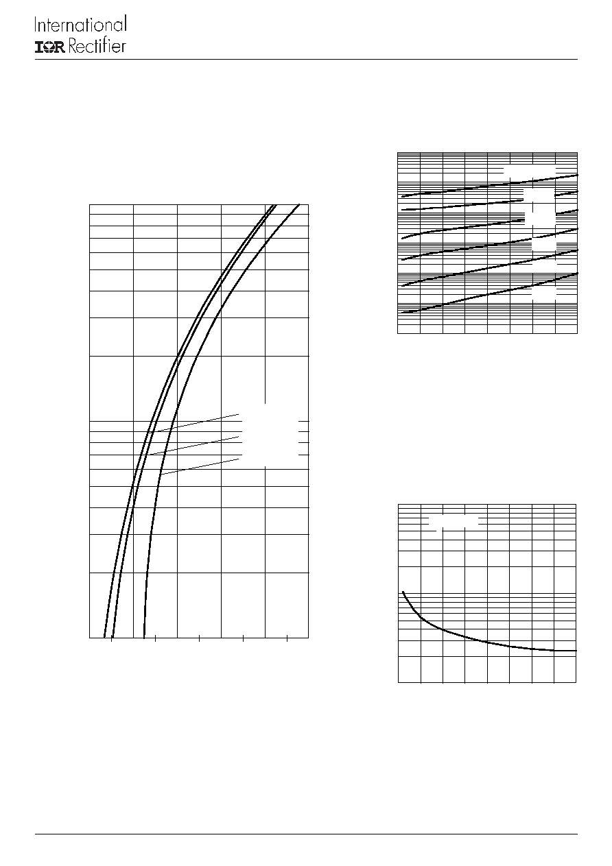
Fig. 2 - Typical Values Of Reverse Current
Vs. Reverse Voltage (Per Leg)
Fig. 3 - Typical Junction Capacitance
Vs. Reverse Voltage (Per Leg)
Fig. 1 - Max. Forward Voltage Drop Characteristics
(Per Leg)
Forward Voltage Drop - V
FM
(V)
Instantaneous Forward Current - I
F
(A)
Reverse Voltage - V
R
(V)
Reverse Current - I
R
(mA)
Reverse Voltage - V
R
(V)
Junction Capacitance - C
T
(p F)
10
100
1000
0
5
10 15 20 25 30 35 40
T = 25°C
J
0.1
1
10
0.2
0.4
0.6
0.8
1
1.2
T = 150°C
T = 125°C
T = 25°C
J
J
J
0.01
0.1
1
10
100
1000
10000
0
5
10 15 20 25 30 35 40
125°C
100°C
75°C
50°C
25°C
Tj = 150°C
IR05H40CSP
Preliminary Data Sheet I0170J rev. A 06/05
4
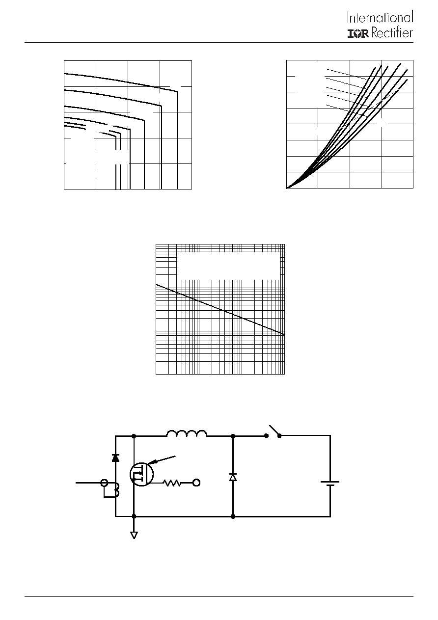
Fig. 6 - Max. Non-Repetitive Surge Current (Per Leg)
Fig. 4 - Max. Allowable Case Temperature
Vs. Average Forward Current (Per Leg)
Fig. 8 - Unclamped Inductive Test Circuit
Fig. 5 - Forward Power Loss Characteristics
(Per Leg)
FREE-WHEEL
DIODE
40HFL40S02
CURRENT
MONITOR
HIGH-SPEED
SWITCH
IRFP460
L
DUT
Rg = 25 ohm
Vd = 25 Volt
+
(2) Formula used: T
C
= T
J
- (Pd + Pd
REV
) x R
thJC
;
Pd = Forward Power Loss = I
F(AV)
x V
FM
@ (I
F(AV)
/
D) (see Fig. 6);
Pd
REV
= Inverse Power Loss = V
R1
x I
R
(1 - D); I
R
@ 80% V
R
applied
Average Forward Current - I
F(AV)
(A)
Allowable Case Temperature (°C)
Average Forward Current - I
F(AV)
(A)
Average Power Loss (Watts)
Square Wave Pulse Duration - t
p
(microsec)
Non-Repetitive Surge Current - I
FSM
(A)
60
80
100
120
140
160
0
0.2
0.4
0.6
0.8
DC
Square wave (D = 0.50)
80% Vr applied
see note (2)
D = 3/4
D = 1/2
D = 1/3
D = 1/4
D = 1/5
0
0.1
0.2
0.3
0.4
0
0.2
0.4
0.6
0.8
DC
RMS Limit
D = 0.20
D = 0.25
D = 0.33
D = 0.50
D = 0.75
1
10
100
1000
10
100
1000
10000
At Any Rated Load Condition
And With Rated Vrrm Applied
Following Surge
IR05H40CSP
Preliminary Data Sheet I0170J rev. A 06/05
5
0.300
0.460
0.355
0.395
1.244
0.105
0.125
0.520
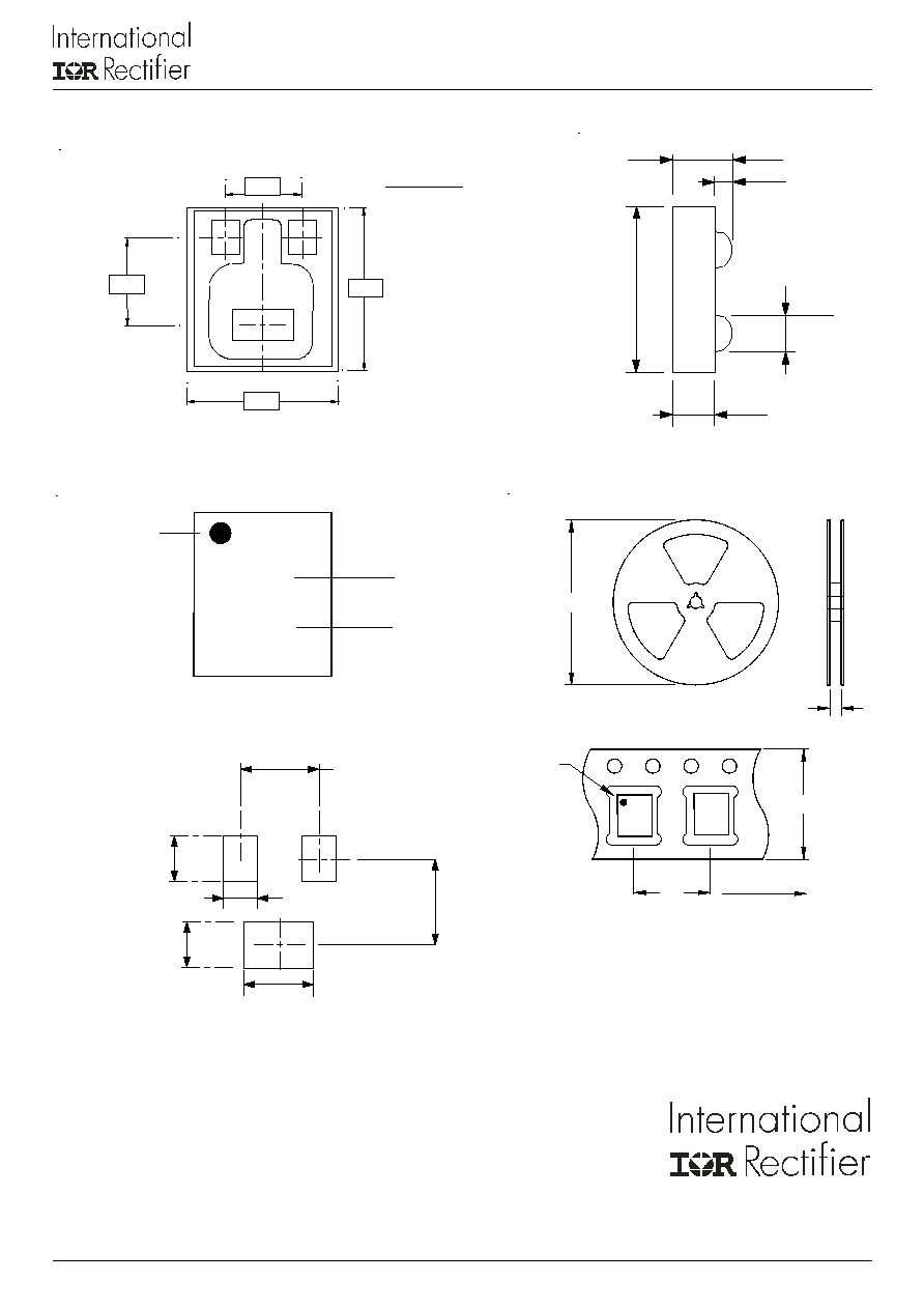
Pin 3 Anode
0.450
0.250
0.350
0.700
Pin 2 Cathode
0.350
Pin 1 Cathode
RECOMMENDED FOOTPRINT
0.500
0.700
1.244
0.914
3. DIMENSIONS ARE SHOWN IN MILLIMETERS
2. CONTROLLING DIMENSION: MILLIMETER
1. DIMENSIONING & TOLERANCING PER ASME Y14.5M-1994.
NOTES:
ASSIGNMENTS
3 = ANODE
2 = CATHODE
1 = CATHODE
3
0.500
2
1
IR WORLD HEADQUARTERS: 233 Kansas St., El Segundo, California 90245, USA Tel: (310) 252-7105
TAC Fax: (310) 252-7309
Visit us at www.irf.com for sales contact information. 06/05
Data and specifications subject to change without notice.
This product has been designed for Consumer Level.
Qualification Standards can be found on IR's Web site.
4mm
1. TAPE AND REEL OUTLINE CONFORMS TO EIA-481 & EIA-541.
NOTES:
FEED DIRECTION
LOCATION
A1 BALL
8mm
8mm
Ø 13"
FlipKY
TM
Outline Dimension and Tape and Reel
BALL 1 MARK
IR
PART NUMBER
54
01
A1
LOT NUMBER