 | ÐлекÑÑоннÑй компоненÑ: IR2105 | СкаÑаÑÑ:  PDF PDF  ZIP ZIP |
Äîêóìåíòàöèÿ è îïèñàíèÿ www.docs.chipfind.ru
Data Sheet No. PD60139J
IR2105
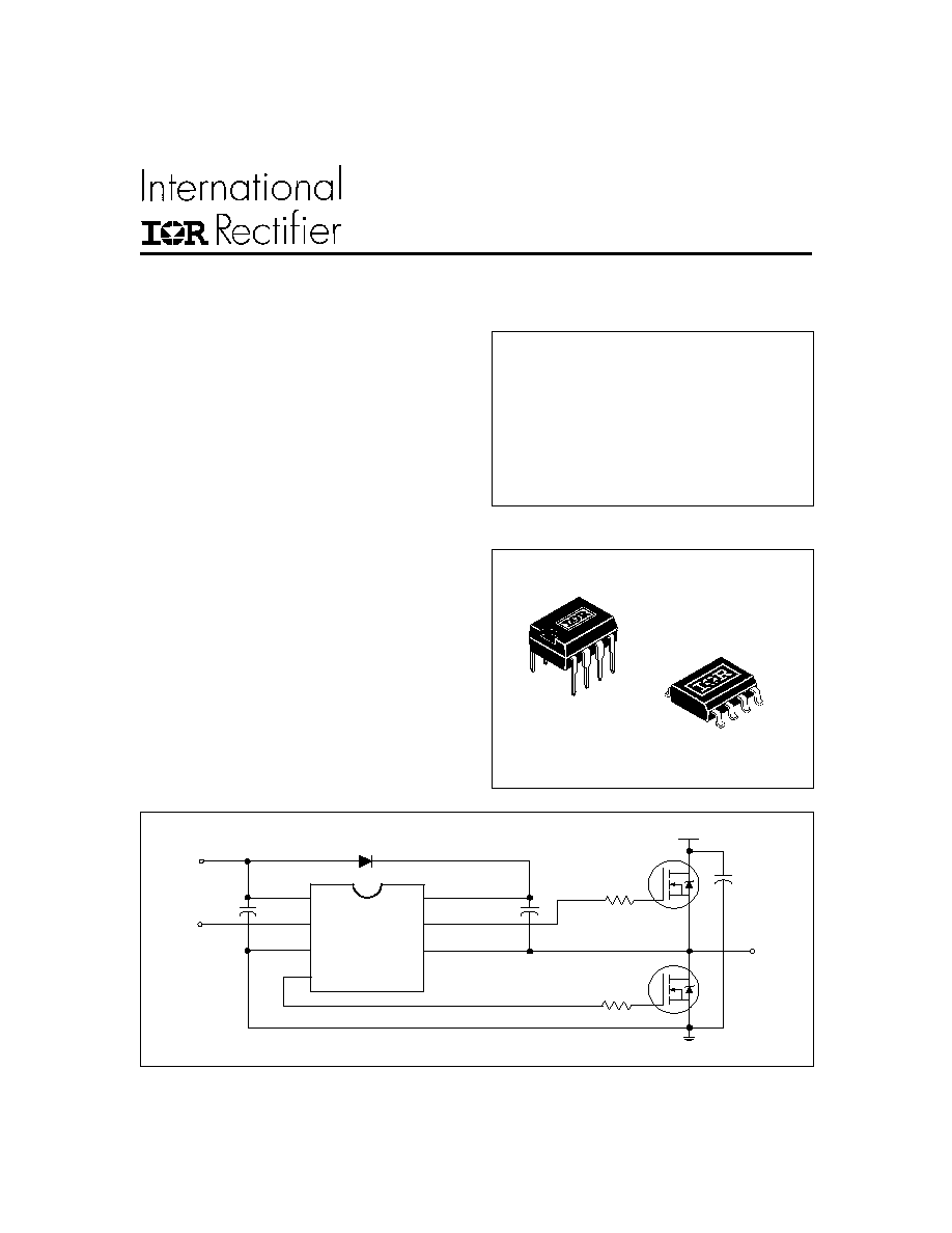
Typical Connection
Packages
Product Summary
V
OFFSET
600V max.
I
O
+/-
130 mA / 270 mA
V
OUT
10 - 20V
t
on/off
(typ.)
680 & 150 ns
Deadtime (typ.)
520 ns
HALF BRIDGE DRIVER
Features
·
Floating channel designed for bootstrap operation
Fully operational to +600V
Tolerant to negative transient voltage
dV/dt immune
·
Gate drive supply range from 10 to 20V
·
Undervoltage lockout
·
5V Schmitt-triggered input logic
·
Cross-conduction prevention logic
·
Internally set deadtime
·
High side output in phase with input
·
Match propagation delay for both channels
Description
The IR2105 is a high voltage, high speed power
MOSFET and IGBT driver with dependent high and
low side referenced output channels. Proprietary
HVIC and latch immune CMOS technologies en-
able ruggedized monolithic construction. The logic
input is compatible with standard CMOS or LSTTL
outputs. The output drivers feature a high pulse
current buffer stage designed for minimum driver
cross-conduction. The floating channel can be used
to drive an N-channel power MOSFET or IGBT in
the high side configuration which operates from 10
to 600 volts.
V
CC
V
B
V
S
HO
LO
COM
IN
IN
up to 600V
TO
LOAD
V
CC
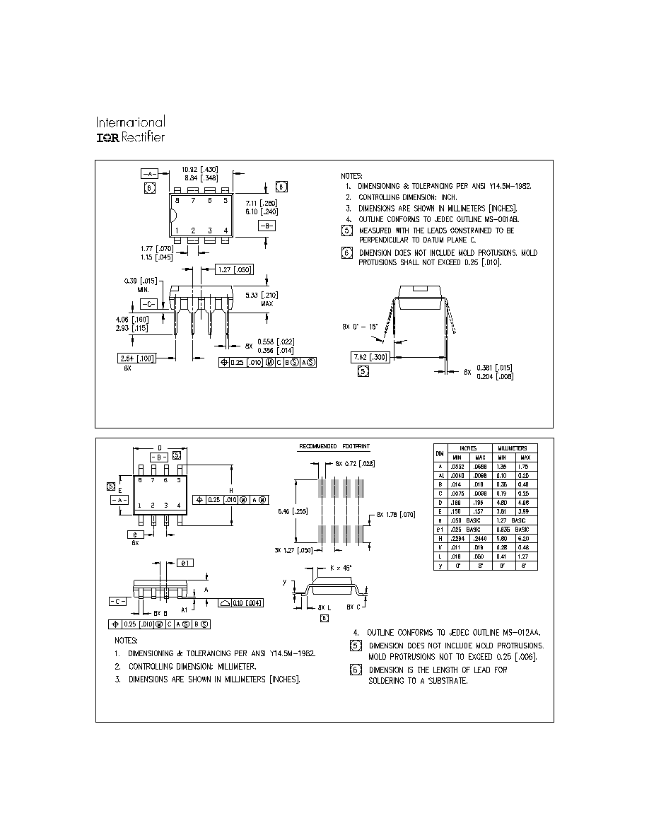
8 Lead PDIP
8 Lead SOIC
2
IR2105
www.irf.com
Symbol Definition
Min.
Max.
Units
V
B
High side floating absolute voltage
-0.3
625
V
S
High side floating supply offset voltage
V
B
- 25
V
B
+ 0.3
V
HO
High side floating output voltage
V
S
- 0.3
V
B
+ 0.3
V
CC
Low side and logic fixed supply voltage
-0.3
25
V
LO
Low side output voltage
-0.3
V
CC
+ 0.3
V
IN
Logic input voltage
-0.3
V
CC
+ 0.3
dV
s
/dt
Allowable offset supply voltage transient
--
50
V/ns
P
D
Package power dissipation @ T
A
+25°C
(8 Lead DIP)
--
1.0
(8 Lead SOIC)
--
0.625
Rth
JA
Thermal resistance, junction to ambient
(8 Lead DIP)
--
125
(8 Lead SOIC)
--
200
T
J
Junction temperature
--
150
T
S
Storage temperature
-55
150
°C
T
L
Lead temperature (soldering, 10 seconds)
--
300
Absolute Maximum Ratings
Absolute maximum ratings indicate sustained limits beyond which damage to the device may occur. All voltage param-
eters are absolute voltages referenced to COM. The thermal resistance and power dissipation ratings are measured
under board mounted and still air conditions.
Symbol Definition
Min.
Max.
Units
V
B
High side floating supply absolute voltage
V
S
+ 10
V
S
+ 20
V
S
High side floating supply offset voltage
Note 1
600
V
HO
High side floating output voltage
V
S
V
B
V
CC
Low side and logic fixed supply voltage
10
20
V
LO
Low side output voltage
0
V
CC
V
IN
Logic input voltage
0
V
CC
T
A
Ambient temperature
-40
125
Note 1: Logic operational for V
S
of -5 to +600V. Logic state held for V
S
of -5V to -V
BS
.
Recommended Operating Conditions
The input/output logic timing diagram is shown in figure 1. For proper operation the device should be used within the
recommended conditions. The V
S
offset rating is tested with all supplies biased at 15V differential.
°C
V
V
W
°C/W
3
IR2105
www.irf.com
Symbol
Definition
Min.
Typ. Max. Units Test Conditions
V
IH
Logic "1" (HO) & Logic "0" (LO) Input Voltage
3
--
--
V
CC
= 10V to 20V
V
IL
Logic "0" (HO) & Logic "1" (LO) Input Voltage
--
--
0.8
V
CC
= 10V to 20V
V
OH
High Level Output Voltage, V
BIAS
- V
O
--
--
100
I
O
= 0A
V
OL
Low Level Output Voltage, V
O
--
--
100
I
O
= 0A
I
LK
Offset Supply Leakage Current
--
--
50
V
B
= V
S
= 600V
I
QBS
Quiescent V
BS
Supply Current
--
30
55
V
IN
= 0V or 5V
I
QCC
Quiescent V
CC
Supply Current
--
150
270
V
IN
= 0V or 5V
I
IN+
Logic "1" Input Bias Current
--
3
10
V
IN
= 5V
I
IN-
Logic "0" Input Bias Current
--
--
1
V
IN
= 0V
V
CCUV+
V
CC
Supply Undervoltage Positive Going
8
8.9
9.8
Threshold
V
CCUV-
V
CC
Supply Undervoltage Negative Going
7.4
8.2
9
Threshold
I
O+
Output High Short Circuit Pulsed Current
130
210
--
V
O
= 0V
PW
10 µs
I
O-
Output Low Short Circuit Pulsed Current
270
360
--
V
O
= 15V
PW
10 µs
Symbol
Definition
Min.
Typ. Max. Units Test Conditions
ton
Turn-on propagation delay
--
680
820
V
S
= 0V
toff
Turn-off propagation delay
--
150
220
V
S
= 600V
tr
Turn-on rise time
--
100
170
tf
Turn-off fall time
--
50
90
DT
Deadtime, LS turn-off to HS turn-on &
400
520
650
HS turn-on to LS turn-off
MT
Delay matching, HS & LS turn-on/off
--
--
60
Static Electrical Characteristics
V
BIAS
(V
CC
, V
BS
) = 15V and T
A
= 25°C unless otherwise specified. The V
IN
, V
TH
and I
IN
parameters are referenced to
COM. The V
O
and I
O
parameters are referenced to COM and are applicable to the respective output leads: HO or LO.
Dynamic Electrical Characteristics
V
BIAS
(V
CC
, V
BS
) = 15V, C
L
= 1000 pF and T
A
= 25°C unless otherwise specified.
V
mV
V
mA
ns
µA
4
IR2105
www.irf.com
Functional Block Diagram
Lead Definitions
Lead
Symbol
Description
IN
Logic input for high and low side gate driver outputs (HO and LO), in phase with HO
V
B
High side floating supply
HO
High side gate drive output
V
S
High side floating supply return
V
CC
Low side and logic fixed supply
LO
Low side gate drive output
COM
Low side return
Lead Assignments
8 Lead PDIP
8 Lead SOIC
IR2105
IR2105S
COM
LO
COM
LO
PULSE
GEN
IN
UV
DETECT
COM
HO
V
S
V
CC
LO
V
B
R
Q
S
PULSE
FILTER
HV
LEVEL
SHIFT
DEAD
TIME
DEAD
TIME
5
5
5
IR2105
www.irf.com
8 Lead PDIP
01-3003 01
8 Lead SOIC
01-0021 08