 | ÐлекÑÑоннÑй компоненÑ: IR2110E4 | СкаÑаÑÑ:  PDF PDF  ZIP ZIP |
Äîêóìåíòàöèÿ è îïèñàíèÿ www.docs.chipfind.ru
Symbol
Parameter
Min.
Max.
Units
V
B
High Side Floating Supply Absolute Voltage
-0.5
V
S
+ 20
V
S
High Side Floating Supply Offset Voltage
--
400
V
HO
High Side Output Voltage
V
S
-0.5
V
B
+ 0.5
V
CC
Low Side Fixed Supply Voltage
-0.5
20
V
LO
Low Side Output Voltage
-0.5
V
CC
+ 0.5
V
DD
Logic Supply Voltage
-0.5
V
SS
+ 20
V
SS
Logic Supply Offset Voltage
V
CC
- 20
V
CC
+ 0.5
V
IN
Logic Input Voltage (HIN, LIN & SD)
V
SS
- 0.5
V
DD
+ 0.5
dV
S
/dt
Allowable Offset Supply Voltage Transient (Fig. 16)
--
50
V/ns
P
D
Package Power Dissipation @ T
A
= 25°C (Fig. 19)
--
1.6
W
R
thJA
Thermal Resistance, Junction to Ambient
--
125
°C/W
T
j
Junction Temperature
-55
125
T
S
Storage Temperature
-55
150
T
L
Package Mounting Surface Temperature
300 (for 5 seconds)
Weight
0.45 (typical)
g
Features
n
Floating channel designed for bootstrap
operation
Fully operational to +400V
Tolerant to negative transient voltage
dV/dt immune
n
Gate drive supply range from 10 to 20V
n
Undervoltage lockout for both channels
n
Separate logic supply range from 5 to 20V
Logic and power ground ±5V offset
n
CMOS Schmitt-triggered inputs with pull-down
n
Cycle by cycle edge-triggered shutdown logic
n
Matched propagation delay for both channels
n
Outputs in phase with inputs
IR2110E4
HIGH AND LOW SIDE DRIVER
Product Summary
V
OFFSET
400V max.
I
O
+/-
2A / 2A
V
OUT
10 - 20V
t
on/off
(typ.)
120 & 94 ns
Delay Matching
10 ns
Absolute Maximum Ratings
Absolute Maximum Ratings indicate sustained limits beyond which damage to the device may occur. All
voltage parameters are absolute voltages referenced to COM. The Thermal Resistance and Power Dissi-
pation ratings are measured under board mounted and still air conditions. Additional information is shown
in Figures 28 through 35.
Description
The IR2110E4 is a high voltage, high speed power MOSFET
and IGBT driver with independent high and low side refer-
enced output channels. Proprietary HVIC and latch immune
CMOS technologies enable ruggedized monolithic construc-
tion. Logic inputs are compatible with standard CMOS or
LSTTL outputs. The output drivers feature a high pulse
current buffer stage designed for minimum driver cross-con-
duction. Propagation delays are matched to simplify use in
high frequency applications. The floating channel can be
used to drive an N-channel power MOSFET or IGBT in the
high side configuration which operates up to 400 volts.
V
°C
4/19/99
www.irf.com
1
PD - 60086B
IR2110E4
2
www.irf.com
Recommended Operating Conditions
The Input/Output logic timing diagram is shown in Figure 1. For proper operation the device should be
used within the recommended conditions. The VS and VSS offset ratings are tested with all supplies
biased at 15V differential. Typical ratings at other bias conditions are shown in Figures 36 and 37.
Symbol
Parameter
Min.
Max.
Units
VB
High Side Floating Supply Absolute Voltage
VS + 10
VS + 20
VS
High Side Floating Supply Offset Voltage
-4
400
VHO
High Side Output Voltage
VS
VB
VCC
Low Side Fixed Supply Voltage
10
20
VLO
Low Side Output Voltage
0
VCC
VDD
Logic Supply Voltage
VSS + 5
VSS + 20
VSS
Logic Supply Offset Voltage
-5
5
VIN
Logic Input Voltage (HIN, LIN & SD)
VSS
VDD
Symbol Parameter
Min
Typ. Max. Min. Max Units
Test Conditions
t
on
Turn-On Propagation Delay
--
120
150
--
260
V
S
= 0V
t
off
Turn-Off Propagation Delay
--
94
125
--
220
V
S
= 400V
t
sd
Shutdown Propagation Delay
--
110
140
--
235
V
S
= 400V
t
r
Turn-On Rise Time
--
25
35
--
50
C
L
= 1000pf
t
f
Turn-Off Fall Time
--
17
25
--
40
C
L
= 1000pf
Mt
Delay Matching, HS & LS Turn-On/Off
--
--
10
--
--
Ht
on
-Lt
on
Ht
off
-Lt
off
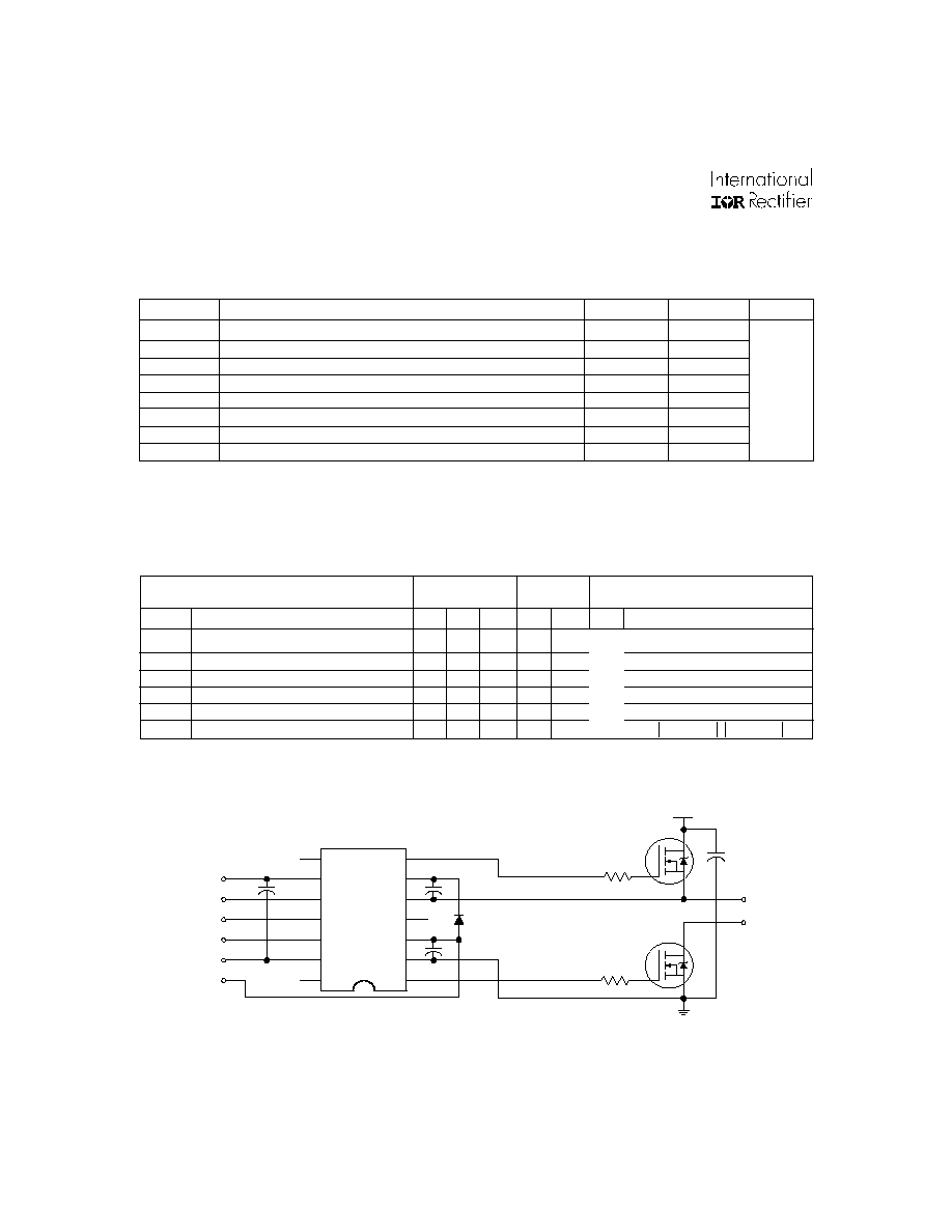
Typical Connection
HIN
up to 500V
TO
LOAD
V
DD
V
B
V
S
HO
LO
COM
HIN
LIN
V
SS
SD
V
CC
LIN
V
DD
SD
V
SS
V
CC
V
Dynamic Electrical Characteristics
VBIAS (VCC, VBS, VDD) = 15V, CL = 1000 pF, TA = 25°C and VSS = COM unless otherwise
specified. The dynamic electrical characteristics are measured using the test circuit shown
in Figure 3.
Tj = 25°C
Tj = -55 to
125°C
nS
4
/
IR2110E4
www.irf.com
3
Symbol Parameter
Min
Typ. Max. Min. Max Units Test Conditions
V
IH
Logic "1" Input Voltage
9.5
--
--
10
--
V
DD
= 15V
V
IL
Logic "0" Input Voltage
--
--
6
--
5.7
V
DD
= 15V
V
OH
High Level Output Voltage, V
BIAS
- V
O
--
0.7
1.2
--
1.5
V
IN
= V
IH
, I
O
= 0A
V
OL
Low Level Output Voltage, VO
--
--
0.1
--
0.1
V
IN
= V
IL
, I
O
= 0A
I
LK
Offset Supply Leakage Current
--
--
50
--
250
V
B
= V
S
= 400V
I
QBS
Quiescent V
BS
Supply Current
--
125
230
--
500
V
IN
= V
IH
or V
IL
I
QCC
Quiescent V
CC
Supply Current
--
180
340
--
600
V
IN
= V
IH
or V
IL
I
QDD
Quiescent V
DD
Supply Current
--
5
30
--
60
V
IN
= V
IH
or V
IL
I
IN+
Logic "1" Input Bias Current
--
15
40
--
70
V
IN
= 15V
I
IN-
Logic "0" Input Bias Current
--
--
1
--
10
V
IN
= 0V
V
BSUV+
V
BS
Supply Undervoltage Positive
7.5
8.7
9.7
--
--
Going Threshold
V
BSUV-
V
BS
Supply Undervoltage Negative
7.0
8.3
9.4
--
--
Going Threshold
V
CCUV+
V
CC
Supply Undervoltage Positive
7.4
8.6
9.6
--
--
Going Threshold
V
CCUV-
V
CC
Supply Undervoltage Negative
7.0
8.2
9.4
--
--
Going Threshold
I
O+
Output High Short Circuit Pulsed
2
--
--
--
--
V
OUT
= 0V, V
IN
= 15V
Current
PW < = 10
I
O-
Output Low Short Circuit Pulsed
2
--
--
--
--
V
OUT
= 15V, V
IN
= 0V
Current
PW < = 10
Static Electrical Characteristics
VBIAS (VCC, VBS, VDD) = 15V, TA = 25°C and VSS = COM unless otherwise specified. The VIN, VTH and
IIN parameters are referenced to VSS and are applicable to all three logic input leads: HIN, LIN and SD.
The VO and IO parameters are referenced to COM and are applicable to the respective output leads: HO or
LO.
Tj = 25°C
Tj = -55 to
125°C
V
V
A
µ
A
µ
s
µ
s
IR2110E4
4
www.irf.com
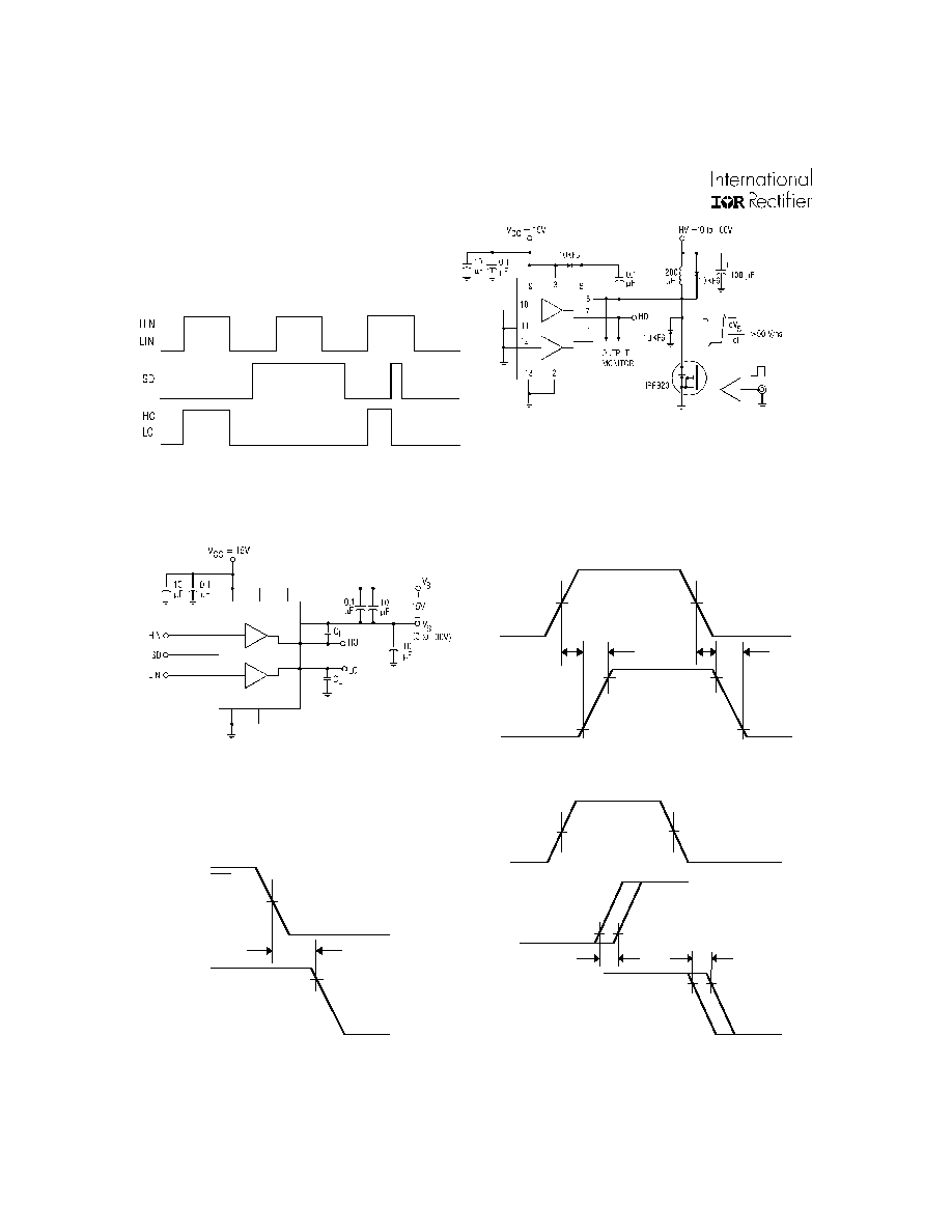
Figure 1. Input/Output Timing Diagram
Figure 2. Floating Supply Voltage Transient Test Circuit
Figure 3. Switching Time Test Circuit
Figure 4. Switching Time Waveform Definition
Figure 6. Delay Matching Waveform Definitions
Figure 3. Shutdown Waveform Definitions
SD
tsd
HO
LO
50%
90%
HIN
LIN
tr
ton
tf
toff
HO
LO
50%
50%
90%
90%
10%
10%
HIN
LIN
HO
50%
50%
10%
LO
90%
MT
HO
LO
MT
4
4
4 8
15
11
13
14
17
2
1
9
6
4
IR2110E4
www.irf.com
5
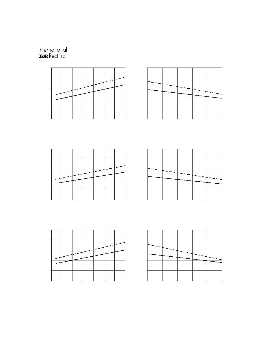
Figure 9B. Shutdown Time vs. Voltage
Figure 8A. Turn-Off Time vs. Temperature
Figure 8B. Turn-Off Time vs. Voltage
Figure 7A. Turn-On Time vs. Temperature
Figure 7B. Turn-On Time vs. Voltage
Figure 9A. Shutdown Time vs. Temperature
0
50
100
150
200
250
10
12
14
16
18
20
V
BIAS
Supply Voltage (V)
Turn-On Delay Time (ns)
Max.
Typ.
0
50
100
150
200
250
-50
-25
0
25
50
75
100
125
Temperature (°C)
Turn-On Delay Time (ns)
Max.
Typ.
0
50
100
150
200
250
-50
-25
0
25
50
75
100
125
Temperature (°C)
Turn-Off Delay Time (ns)
Max.
Typ.
0
50
100
150
200
250
10
12
14
16
18
20
V
BIAS
Supply Voltage (V)
Turn-Off Delay Time (ns)
Max.
Typ.
0
50
100
150
200
250
10
12
14
16
18
20
V
BIAS
Supply Voltage (V)
Shutdown Delay time (ns)
Max.
Typ.
0
50
100
150
200
250
-50
-25
0
25
50
75
100
125
Temperature (°C)
Shutdown Delay Time (ns)
Max.
Typ.