 | ÐлекÑÑоннÑй компоненÑ: IR2128 | СкаÑаÑÑ:  PDF PDF  ZIP ZIP |
Äîêóìåíòàöèÿ è îïèñàíèÿ www.docs.chipfind.ru
Features
n
Floating channel designed for bootstrap operation
Fully operational to +600V
Tolerant to negative transient voltage
dV/dt immune
n
Gate drive supply range from 10 to 20V
n
Undervoltage lockout
n
5V Schmitt-triggered input logic
n
FAULT lead indicates shutdown has occured
n
Output out of phase with input
Description
The IR2128 is a high voltage, high speed power
MOSFET and IGBT driver. Proprietary HVIC and
latch immune CMOS technologies enable rugge-
dized monolithic construction. The logic input is
compatible with standard CMOS or LSTTL outputs.
The protection circuity detects over-current in the
driven power transistor and terminates the gate
drive voltage. An open drain FAULT signal is pro-
vided to indicate that an over-current shutdown has
occurred. The output driver features a high pulse
current buffer stage designed for minimum cross-
conduction. The floating channel can be used to
drive an N-channel power MOSFET or IGBT in the
high side or low side configuration which operates
up to 600 volts.
Data Sheet No. PD-6.042D
IR2128
CURRENT SENSING SINGLE CHANNEL DRIVER
Product Summary
V
OFFSET
600V max.
I
O
+/-
200 mA / 420 mA
V
OUT
10 - 20V
V
CSth
250 mV
t
on/off
(typ.)
150 & 100 ns
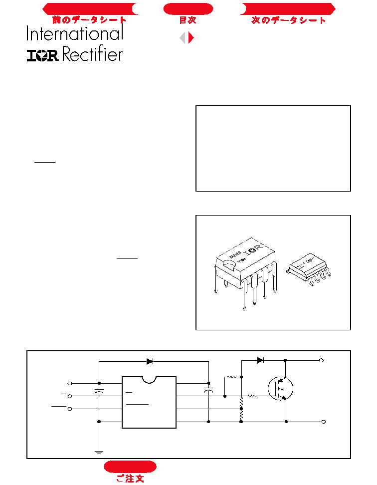
Typical Connection
Packages
V
CC
V
B
CS
HO
V
S
COM
IN
FAULT
V
CC
IN
FAULT
C
ONTROL
I
NTEGRATED
C
IRCUIT
D
ESIGNERS
M
ANUAL
B-129
Next Data Sheet
Index
Previous Datasheet
To Order
IR2128
B-130 C
ONTROL
I
NTEGRATED
C
IRCUIT
D
ESIGNERS
M
ANUAL
Parameter
Value
Symbol
Definition
Min.
Max.
Units
V
B
High Side Floating Supply Voltage
-0.3
625
V
S
High Side Floating Offset Voltage
V
B
- 25
V
B
+ 0.3
V
HO
High Side Floating Output Voltage
V
S
- 0.3
V
B
+ 0.3
V
CC
Logic Supply Voltage
-0.3
25
V
V
IN
Logic Input Voltage
-0.3
V
CC
+ 0.3
V
FLT
FAULT
Output Voltage
-0.3
V
CC
+ 0.3
V
CS
Current Sense Voltage
V
S
- 0.3
V
B
+ 0.3
dV
s
/dt
Allowable Offset Supply Voltage Transient
--
50
V/ns
P
D
Package Power Dissipation @ T
A
+25°C
(8 Lead DIP)
--
1.0
(8 Lead SOIC)
--
0.625
R
JA
Thermal Resistance, Junction to Ambient
(8 Lead DIP)
--
125
(8 Lead SOIC)
--
200
T
J
Junction Temperature
--
150
T
S
Storage Temperature
-55
150
°C
T
L
Lead Temperature (Soldering, 10 seconds)
--
300
Absolute Maximum Ratings
Absolute Maximum Ratings indicate sustained limits beyond which damage to the device may occur. All voltage param-
eters are absolute voltages referenced to COM. The Thermal Resistance and Power Dissipation ratings are measured
under board mounted and still air conditions.
Parameter
Value
Symbol
Definition
Min.
Max.
Units
V
B
High Side Floating Supply Voltage
V
S
+ 10
V
S
+ 20
V
S
High Side Floating Offset Voltage
Note 1
600
V
HO
High Side Floating Output Voltage
V
S
V
B
V
CC
Logic Supply Voltage
11.8
20
V
V
IN
Logic Input Voltage
0
V
CC
V
FLT
FAULT
Output Voltage
0
V
CC
V
CS
Current Sense Signal Voltage
V
S
V
S
+ 5
T
A
Ambient Temperature
-40
125
°C
Note 1: Logic operational for V
S
of -5 to +600V. Logic state held for V
S
of -5V to -V
BS
.
Recommended Operating Conditions
The Input/Output logic timing diagram is shown in Figure 1. For proper operation the device should be used within the
recommended conditions. The V
S
offset rating is tested with all supplies biased at 15V differential.
°C/W
W
Next Data Sheet
Index
Previous Datasheet
To Order
IR2128
C
ONTROL
I
NTEGRATED
C
IRCUIT
D
ESIGNERS
M
ANUAL
B-131
Parameter
Value
Symbol
Definition
Min.
Typ. Max. Units Test Conditions
V
IH
Logic "0" Input Voltage (OUT = LO)
2.7
--
--
V
CC
= 10V to 20V
V
IL
Logic "1" Input Voltage (OUT = HI)
--
--
0.8
V
CC
= 10V to 20V
V
CSTH+
CS Input Positive Going Threshold
180
250
320
V
CC
= 10V to 20V
V
OH
High Level Output Voltage, V
BIAS
- V
O
--
--
100
mV
I
O
= 0A
V
OL
Low Level Output Voltage, V
O
--
--
100
I
O
= 0A
I
LK
Offset Supply Leakage Current
--
--
50
V
B
= V
S
= 600V
I
QBS
Quiescent V
BS
Supply Current
--
150
300
V
IN
= 0V or 5V
I
QCC
Quiescent V
CC
Supply Current
--
60
120
V
IN
= 0V or 5V
I
IN+
Logic "1" Input Bias Current
--
7.0
15
µA
V
IN
= 0V
I
IN-
Logic "0" Input Bias Current
--
--
1.0
V
IN
= 5V
I
CS+
"High" CS Bias Current
--
--
1.0
V
CS
= 3V
I
CS-
"High" CS Bias Current
--
--
1.0
V
CS
= 0V
V
BSUV+
V
BS
Supply Undervoltage Positive Going
8.8
10.3
11.8
Threshold
V
BSUV-
V
BS
Supply Undervoltage Negative Going
7.5
9.0
10.6
Threshold
I
O+
Output High Short Circuit Pulsed Current
200
250
--
V
O
= 0V, V
IN
= 0V
PW
10 µs
I
O-
Output Low Short Circuit Pulsed Current
420
500
--
V
O
= 15V, V
IN
= 5V
PW
10 µs
Parameter
Value
Symbol
Definition
Min.
Typ. Max. Units Test Conditions
t
on
Turn-On Propagation Delay
--
150
200
V
S
= 0V
t
off
Turn-Off Propagation Delay
--
100
150
V
S
= 600V
t
r
Turn-On Rise Time
--
80
120
C
L
= 1000 pF
t
f
Turn-Off Fall Time
--
40
60
ns
C
L
= 1000 pF
t
bl
Start-Up Blanking Time
500
750
900
t
cs
CS Shutdown Propagation Delay
--
240
360
t
flt
CS to FAULT Pull-Up Propagation Delay
--
340
510
Dynamic Electrical Characteristics
V
BIAS
(V
CC
, V
BS
) = 15V, C
L
= 1000 pF and T
A
= 25°C unless otherwise specified. The dynamic electrical characteristics
are measured using the test circuit shown in Figure 3.
Static Electrical Characteristics
V
BIAS
(V
CC
, V
BS
) = 15V and T
A
= 25°C unless otherwise specified. The V
IN
, V
TH
and I
IN
parameters are referenced to
COM. The V
O
and I
O
parameters are referenced to V
S
.
mA
V
V
To Order
Next Data Sheet
Index
Previous Datasheet
IR2128
B-132 C
ONTROL
I
NTEGRATED
C
IRCUIT
D
ESIGNERS
M
ANUAL
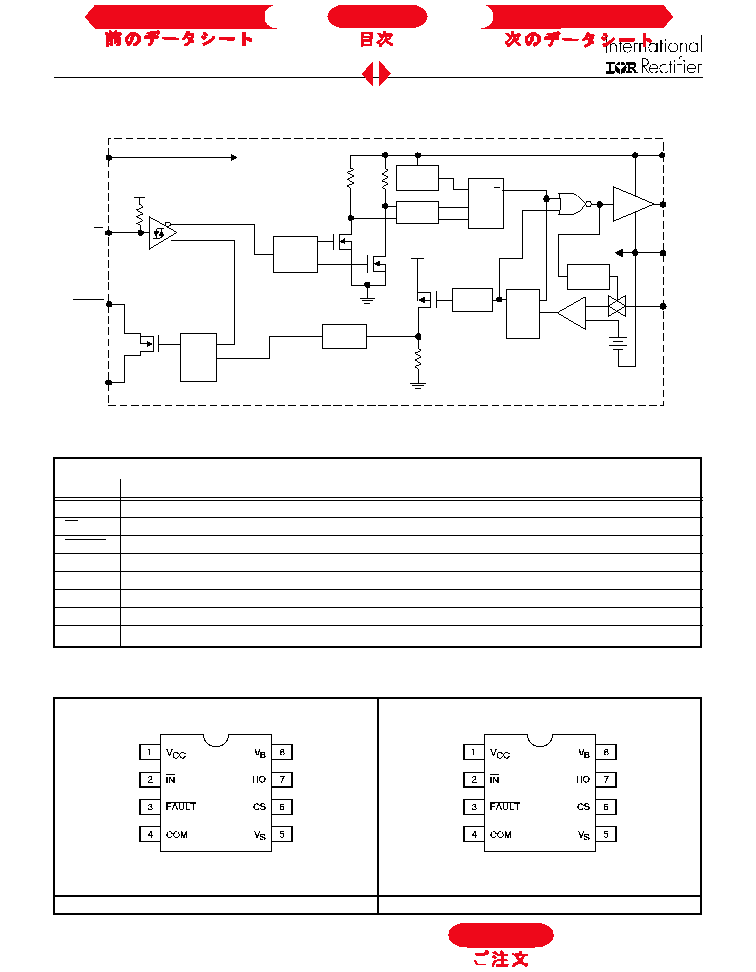
D O W N
SHIFTER
P U L S E
G E N
U V
DETECT
P U L S E
FILTER
P U L S E
G E N
B U F F E R
H V
L E V E L
V
B
H O
V
S
C S
R
S
R
Q
V
C C
IN
U P
SHIFTERS
C O M
FAULT
-
+
P U L S E
FILTER
V
B
D E L A Y
S
Q
R
Q
R
S
S H I F T
5 V
Lead Definitions
Lead
Symbol
Description
V
CC
Logic and gate drive supply
Logic input for gate driver output (HO), out of phase with HO
Indicates over-current shutdown has occurred, negative logic
COM
Logic ground
V
B
High side floating supply
HO
High side gate drive output
V
S
High side floating supply return
CS
Current sense input to current sense comparator
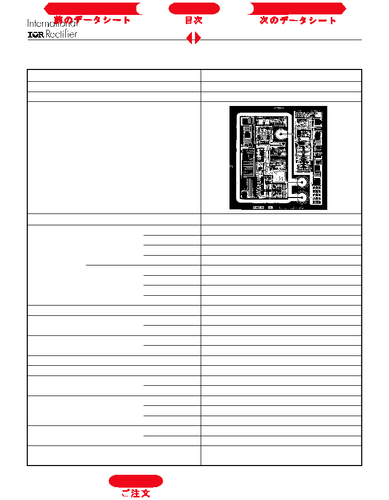
Functional Block Diagram
Lead Assignments
8 Lead DIP
SO-8
IR2128
IR2128S
FAULT
IN
To Order
Next Data Sheet
Index
Previous Datasheet
IR2128
C
ONTROL
I
NTEGRATED
C
IRCUIT
D
ESIGNERS
M
ANUAL
B-133
Thickness of Gate Oxide
800
Å
Connections
Material
Poly Silicon
First
Width
4 µm
Layer
Spacing
6 µm
Thickness
5000Å
Material
Al - Si (Si: 1.0% ±0.1%)
Second
Width
6 µm
Layer
Spacing
7 µm
Thickness
20,000Å
Contact Hole Dimension
8 µm X 8 µm
Insulation Layer
Material
PSG (SiO
2
)
Thickness
1.5 µm
Passivation
Material
PSG (SiO
2
)
Thickness
1.5 µm
Method of Saw
Full Cut
Method of Die Bond
Ablebond 84 - 1
Wire Bond
Method
Thermo Sonic
Material
Au (1.0 mil / 1.3 mil)
Leadframe
Material
Cu
Die Area
Ag
Lead Plating
Pb : Sn (37 : 63)
Package
Types
8 Lead PDIP / SO-8
Materials
EME6300 / MP150 / MP190
Remarks:
Device Information
Process & Design Rule
HVDCMOS 4.0 µm
Transistor Count
206
Die Size
77 X 85 X 26 (mil)
Die Outline
To Order
Next Data Sheet
Index
Previous Datasheet