 | ÐлекÑÑоннÑй компоненÑ: IR21368 | СкаÑаÑÑ:  PDF PDF  ZIP ZIP |
Äîêóìåíòàöèÿ è îïèñàíèÿ www.docs.chipfind.ru
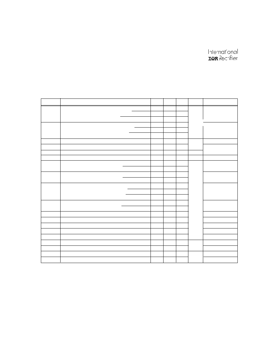
Typical Connection
3-PHASE BRIDGE DRIVER
Features
·
Floating channel designed for bootstrap operation
Fully operational to +600V
Tolerant to negative transient voltage - dV/dt immune
·
Gate drive supply range from 10 to 20V (IR2136/IR21368),
11.5 to 20V (IR21362) or 12 to 20V (IR21363/IR21365/
IR21366/IR21367)
·
Undervoltage lockout for all channels
·
Over-current shutdown turns off all six drivers
·
Independent 3 half-bridge drivers
·
Matched propagation delay for all channels
·
Cross-conduction prevention logic
·
Lowside outputs out of phase with inputs. High side
outputs out of phase (IR2136/IR21363/IR21365/
IR21366/IR21367/IR21368) or in phase
(IR21362) with inputs.
·
3.3V logic compatible
·
Lower di/dt gate driver for
better noise immunity
·
Externally programmable
delay for automatic fault
clear
·
Also available LEAD-FREE
Data Sheet No. PD60166
revS
IR2136/IR21362/IR21363/IR21365/
IR21366/IR21367/IR21368 (J&S) & (PbF)
www.irf.com
1
(Refer to Lead Assign-
ments for correct pin con-
figuration). This/These
diagram(s) show electri-
cal connections only.
Please refer to our Appli-
cation Notes and
DesignTips for proper cir-
cuit board layout.
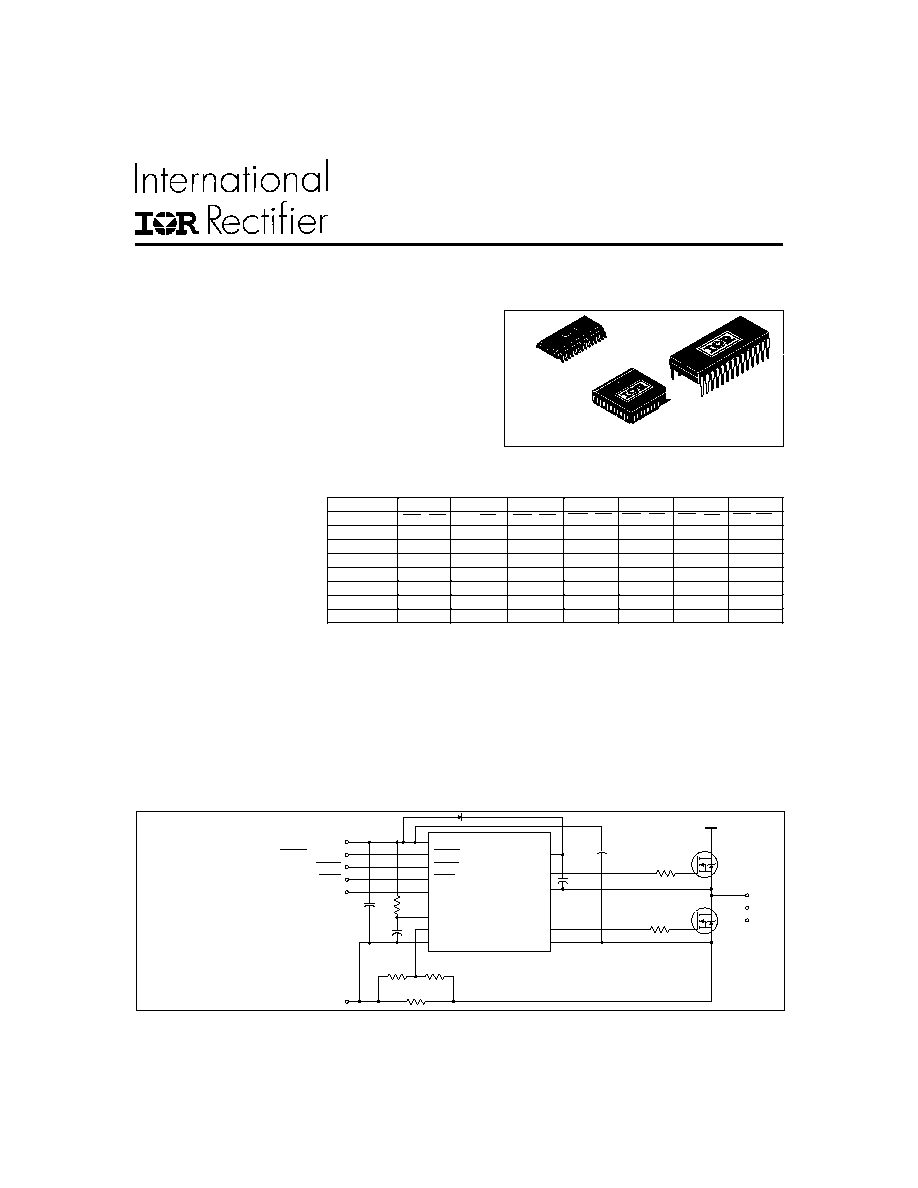
Packages
28-Lead PDIP
28-Lead SOIC
44-Lead PLCC w/o 12 leads
Description
The IR2136/IR21362/IR21363/IR21365/IR21366/IR21367/IR21368(J&S) are high votage, high speed power MOSFET
and IGBT drivers with three independent high and low side referenced output channels for 3-phase applications.
Proprietary HVIC technology enables ruggedized monolithic construction. Logic inputs are compatible with CMOS
or LSTTL outputs, down to 3.3V logic. A current trip function which terminates all six outputs can be derived from
an external current sense resistor. An enable function is available to terminate all six outputs simultaneously. An
open-drain FAULT signal is provided to indicate that an overcurrent or undervoltage shutdown has occurred.
Overcurrent fault conditions are cleared automatically after a delay programmed externally via an RC network
connected to the RCIN input. The output drivers feature a high pulse current buffer stage designed for minimum
driver cross-conduction. Propagation delays are matched to simplify use in high frequency applications. The
floating channel can be used to drive N-channel power MOSFETs or IGBTs in the high side configuration which
operates up to 600 volts.
VCC
HIN1,2,3 / HIN1,2,3
LIN1,2,3
FAULT
ITRIP
RCIN
EN
VSS
COM
LO1,2,3
VS1,2,3
HO1,2,3
VB1,2,3
IR2136(2)(3)(5)(6)(7)(8)
TO
LOAD
VCC
HIN1,2,3 / HIN1,2,3
LIN1,2,3
FAULT
EN
GND
up to 600V
Part
Input Logic
Ton (typ.)
Toff (typ.)
V
IH
(typ.)
V
IL
(typ.)
Vitrip+
UV CC/BS+
UV CC/BS-
IR2136
HIN, LIN
400ns
380ns
2.7V
1.7V
0.46V
8.9V
8.2V
IR21362
HIN/LIN
400ns
380ns
2.7V
1.7V
0.46V
10.4V
9.4V
IR21363
HIN, LIN
400ns
380ns
2.7V
1.7V
0.46V
11.2V
11.0V
IR21365
HIN, LIN
400ns
380ns
2.7V
1.7V
4.3V
11.2V
11.0V
IR21366
HIN, LIN
250ns
180ns
2.0V
1.3V
0.46V
11.2V
11.0V
IR21367
HIN, LIN
250ns
180ns
2.0V
1.3V
4.3V
11.2V
11.0V
IR21368
HIN,LIN
400ns
380ns
2.0V
1.3V
4.3V
8.9V
8.2V
Feature Comparison: IR2136/IR21362/IR21363/
IR21365/IR21366/IR21367/IR21368
IR2136(2)(3)(5)(6)(7)(8)(J&S) & (PbF)
2
www.irf.com
Recommended Operating Conditions
The Input/Output logic timing diagram is shown in figure 1. For proper operation the device should be used within the recom-
mended conditions. All voltage parameters are absolute referenced to COM. The VS offset rating is tested with all supplies
biased at 15V differential.
V
B1,2,3
High side floating supply voltage IR2136(8)
V
S1,2,3 +
10
V
S1,2,3 +
20
IR21362
V
S1,2,3 +
11.5 V
S1,2,3 +
20
IR2136(3)(5)(6)(7)
V
S1,2,3 +
12
V
S1,2,3 +
20
V
S1,2,3
High side floating supply offset voltage
Note 1
600
V
HO1,2,3
High side output voltage
V
S1,2,3
V
B1,2,3
V
LO1,2,3
Low side output voltage
0
V
CC
V
CC
Low side and logic fixed supply voltage IR2136(8)
10
20
IR21362
11.5
20
IR2136(3)(5)(6)(7)
12
20
V
SS
Logic ground
-5
5
V
FLT
FAULT output voltage
V
SS
V
CC
V
RCIN
RCIN input voltage
V
SS
V
CC
Symbol
Definition
Min.
Max.
Units
V
Note 1: Logic operational for V
S
of COM -5V to COM +600V. Logic state held for V
S
of COM -5V to COM -V
BS
.
(Please refer to the Design Tip DT97-3 for more details).
Note 2: All input pins and the ITRIP pin are internally clamped with a 5.2V zener diode.
Symbol
Definition
Min.
Max.
Units
V
S
High side offset voltage
V
B1,2,3
- 25
V
B1,2,3
+ 0.3
V
BS
High side floating supply voltage
-0.3
625
V
HO
High side floating output voltage
V
S1,2,3
- 0.3
V
B1,2,3
+ 0.3
V
CC
Low side and logic fixed supply voltage
-0.3
25
V
SS
Logic ground
V
CC
- 25
V
CC
+ 0.3
V
LO1,2,3
Low side output voltage
-0.3
V
CC
+ 0.3
V
IN
Input voltage LIN,HIN,ITRIP, EN, RCIN
V
SS
- 0.3
lower of
(V
SS
+ 15) or
V
CC
+ 0.3)
V
FLT
FAULT output voltage
V
SS
- 0.3
V
CC
+ 0.3
dV/dt
Allowable offset voltage slew rate
--
50
V/ns
P
D
Package power dissipation @ T
A
+25
°C
(28 lead PDIP)
--
1.5
(28 lead SOIC)
--
1.6
( 44leadPLCC)
--
2.0
Rth
JA
Thermal resistance, junction to ambient
(28 lead PDIP)
--
83
(28 lead SOIC)
--
78
(44 lead PLCC)
--
63
T
J
Junction temperature
--
150
T
S
Storage temperature
-55
150
T
L
Lead temperature (soldering, 10 seconds)
--
300
V
°C/W
Absolute Maximum Ratings
Absolute maximum ratings indicate sustained limits beyond which damage to the device may occur. All voltage parameters
are absolute voltages referenced to COM. The thermal resistance and power dissipation ratings are measured under board
mounted and still air conditions.
W
°C
www.irf.com
3
IR2136(2)(3)(5)(6)(7)(8)(J&S) & (PbF)
Note 2: All input pins and the ITRIP pin are internally clamped with a 5.2V zener diode.
Recommended Operating Conditions cont.
The Input/Output logic timing diagram is shown in figure 1. For proper operation the device should be used within the recom-
mended conditions. All voltage parameters are absolute referenced to COM. The VS offset rating is tested with all supplies
biased at 15V differential.
Symbol
Definition
Min.
Max.
Units
V
Static Electrical Characteristics
V
BIAS
(V
CC
, V
BS
1,2,3) = 15V unless otherwise specified. The V
IN
, V
TH
and I
IN
parameters are referenced to V
SS
and
are applicable to all six channels (H
S
1,2,3 and L
S
1,2,3). The V
O
and I
O
parameters are referenced to COM and V
S
1,2,3
and are applicable to the respective output leads: H
O1,2,3
and L
O1,2,3.
Symbol
Definition
Min. Typ. Max. Units Test Conditions
V
IH
Logic "0" input voltage LIN1,2,3, HIN1,2,3
IR2136(3)(5)
3.0
--
--
Logic "1" input voltage HIN1,2,3
IR21362
Logic "0" input voltage LIN1,2,3, HIN1,2,3
IR21366(7)(8)
2.5
--
--
V
IL
Logic "1" input voltage LIN1,2,3, HIN1,2,3
IR2136(3)(5)
--
--
0.8
Logic "0" input voltage HIN1,2,3
IR21362
Logic "0" input voltage LIN1,2,3, HIN1,2,3
IR21366(7)(8)
--
--
0.8
V
EN,TH+
EN positive going threshold
--
--
3
V
EN,TH-
EN negative going threshold
0.8
--
--
V
IT,TH+
ITRIP positive going threshold
IR2136(2)(3)(6)
0.37
0.46
0.55
IR21365(7)(8)
3.85
4.30
4.75
V
IT,HYS
ITRIP input hysteresis
IR2136(2)(3)(6)
--
0.07
--
IR21365(7)(8)
--
.15
--
V
RCIN,TH+
RCIN positive going threshold
--
8
--
V
RCIN,HYS
RCIN input hysteresis
--
3
--
V
OH
High level output voltage, V
BIAS
- V
O
--
0.9
1.4
I
O
= 20 mA
V
OL
Low level output voltage, V
O
--
0.4
0.6
I
O
= 20 mA
V
CCUV+
V
CC
and V
BS
supply undervoltage IR2136(8)
8.0
8.9
9.8
V
BSUV+
positive going threshold IR21362
9.6
10.4
11.2
IR21363(5)(6)(7)
10.6
11.1
11.6
V
V
ITRIP
ITRIP input voltage
V
SS
V
SS
+5
V
IN
Logic input voltage
LIN
, HIN (IR2136,IR21363(5)(6)(7)(8)),
HIN(IR21362), EN
V
SS
V
SS
+5
T
A
Ambient temperature
-40
125
o
C
IR2136(2)(3)(5)(6)(7)(8)(J&S) & (PbF)
4
www.irf.com
Static Electrical Characteristics cont.
V
BIAS
(V
CC
, V
BS
1,2,3) = 15V unless otherwise specified. The V
IN
, V
TH
and I
IN
parameters are referenced to V
SS
and
are applicable to all six channels (H
S
1,2,3 and L
S
1,2,3). The V
O
and I
O
parameters are referenced to COM and V
S
1,2,3
and are applicable to the respective output leads: H
O1,2,3
and L
O1,2,3.
Symbol
Definition
Min. Typ. Max. Units Test Conditions
V
CCUV-
V
CC
and V
BS
supply undervoltage IR2136(8)
7.4
8.2
9.0
V
BSUV-
negative going threshold
IR21362
8.6
9.4
10.2
IR21363(5)(6)(7)
10.4
10.9
11.4
V
CCUVH
V
CC
and V
BS
supply undervoltage
IR2136
0.3
0.7
--
V
BSUVH
lockout hysteresis
IR21362
0.5
1.0
--
IR21363(5)
--
0.2
--
I
LK
Offset supply leakage current
--
--
50
V
B1,2,3
=V
S1,2,3
=600V
I
QBS
Quiescent V
BS
supply current
--
70
120
I
QCC
Quiescent V
CC
supply current
--
1.6
2.3
mA
V
IN, CLAMP
Input clamp voltage (HIN, LIN, ITRIP and EN)
4.9
5.2
5.5
V
I
IN
=100
µ
A
I
LIN+
Input bias current (LOUT = HI) IR2136(2)(3)(5)
--
200
300
V
LIN
= 5V
IR21366(7)(8)
--
0
1
I
LIN-
Input bias current (LOUT = LO) IR2136(2)(3)(5)
--
100
220
V
LIN
= 0V
IR21366(7)(8)
--
0
1
I
HIN+
Input bias current (HOUT = HI)
IR2136(3)(5)
--
200
300
V
HIN
= 5V
IR21362
--
30
100
IR21366(7)(8)
--
0
1
I
HIN-
Input bias current (HOUT = LO)
IR2136(3)(5)
--
100
220
V
HIN
= 0V
IR21362(6)(7)(8)
--
0
1
I
ITRIP+
"high" ITRIP input bias current
--
30
100
V
ITRIP
= 5V
I
ITRIP-
"low" ITRIP input bias current
--
0
1
V
ITRIP
= 0V
I
EN+
"high" ENABLE input bias current
--
30
100
V
ENABLE
= 5V
I
EN-
"low" ENABLE input bias current
--
0
1
V
ENABLE
= 0V
I
RCIN
RCIN input bias current
--
0
1
V
RCIN
= 0V or 15V
I
O+
Output high short circuit pulsed current
120
200
--
V
O
=0V, PW
10
µs
I
O-
Output low short circuit pulsed current
250
350
--
V
O
=15V, PW
10
µs
R
ON,RCIN
RCIN low on resistance
--
50
100
R
ON,FLT
FAULT low on resistance
--
50
100
V
IN
= 0V or 5V
µ
A
µ
A
mA
V
www.irf.com
5
IR2136(2)(3)(5)(6)(7)(8)(J&S) & (PbF)
VCC
VBS
ITRIP
ENABLE
FAULT
LO1,2,3
HO1,2,3
<UVCC
X
X
X
0 (note 1)
0
0
15V <UVBS
0V
5V
high imp
LIN1,2,3
0
15V
15V
0V
5V
high imp
LIN1,2,3
HIN1,2,3
15V
15V
>VITRIP
5V
0 (note 2)
0
0
15V
15V
0V
0V
high imp
0
0
Note: A shoot-through prevention logic prevents LO1,2,3 and HO1,2,3 for each channel from turning on simultaneously.
Note 1: UVCC is not latched, when VCC>UVCC, FAULT returns to high impedance.
Note 2: When ITRIP <V
ITRIP
, FAULT returns to high-impedance after RCIN pin becomes greater than 8V (@ VCC = 15V)
NOTE: For high side PWM, HIN pulse width must be
1µ
sec
Dynamic Electrical Characteristics
V
CC
= V
BS
= V
BIAS
= 15V, V
S1,2,3
= V
SS
= COM, TA = 25
o
C and C
L
= 1000 pF unless otherwise specified.
Symbol
Definition
Min. Typ.
Max. Units Test Conditions
ton
Turn-on propagation delay IR2136(2)(3)(5)(8)
300
425
550
IR21366(7)
--
250
--
toff
Turn-off propagation delay
IR2136(2)(3)(5)(8)
250
400
550
IR21366(7)
--
180
--
tr
Turn-on rise time
--
125
190
tf
Turn-off fall time
--
50
75
tEN
ENABLE low to output
IR2136(2)(3)(5)(8)
300
450
600
V
IN,
V
EN
= 0V or 5V
shutdown propagation delay IR21366(7)
100
250
400
tITRIP
ITRIP to output shutdown propagation delay
500
750
1000
V
ITRIP
= 5V
tbl
ITRIP blanking time
100
150
--
V
IN
= 0V or 5V
V
ITRIP
= 5V
tFLT
ITRIP to FAULT propagation delay
400
600
800
V
IN
= 0V or 5V
V
ITRIP
= 5V
tFILIN
Input filter time (HIN, LIN, EN)
100
200
--
V
IN
= 0 & 5V
(IR2136(2)(3)(5)(8) only)
tFLTCLR
FAULT clear time RCIN: R=2meg, C=1nF
1.3
1.65
2
mS
V
IN
= 0V or 5V
V
ITRIP
= 0V
DT
Deadtime
220
290
360
V
IN
= 0 & 5V
MT
Matching delay ON and OFF
--
40
75
MDT
Matching delay, max (ton,toff) - min (ton,toff),
--
25
70
(ton,toff are applicable to all 3 channels)
PM
Output pulse width matching, PWin -PWout (fig.2)
--
40
75
nS
V
IN
= 0 & 5V
nS
External dead
time
>400nsec
IR2136(2)(3)(5)(6)(7)(8)(J&S) & (PbF)
6
www.irf.com
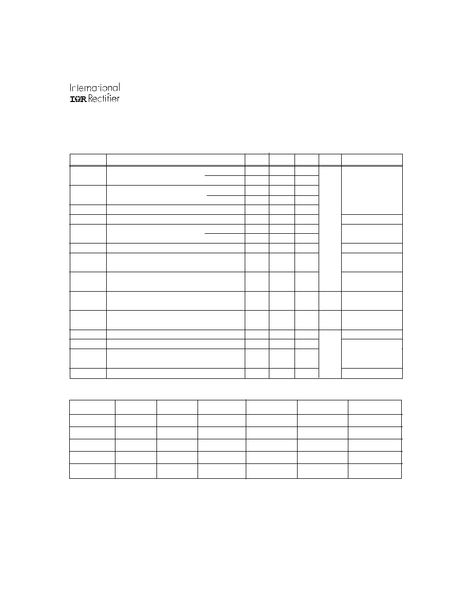
Functional Block Diagram
IR2136/21363/21365
COM
VCC
LO1
LO2
LO3
DELAY
VSS/COM
LEVEL
SHIFTER
DELAY
VSS/COM
LEVEL
SHIFTER
DELAY
VSS/COM
LEVEL
SHIFTER
LIN1
HIN1
LIN2
HIN2
LIN3
HIN3
DEADTIME &
SHOOT-THROUGH
PREVENTION
DEADTIME &
SHOOT-THROUGH
PREVENTION
DEADTIME &
SHOOT-THROUGH
PREVENTION
VS1
HO1
VB1
HV
LEVEL
SHIFTER
VSS/COM
LEVEL
SHIFTER
LATCH
UV
DETECT
SET
RESET
DRIVER
VS2
HO2
VB2
HV
LEVEL
SHIFTER
VSS/COM
LEVEL
SHIFTER
LATCH
UV
DETECT
SET
RESET
DRIVER
VS3
HO3
VB3
HV
LEVEL
SHIFTER
VSS/COM
LEVEL
SHIFTER
LATCH
UV
DETECT
SET
RESET
DRIVER
DRIVER
DRIVER
DRIVER
INPUT
NOISE
FILTER
INPUT
NOISE
FILTER
INPUT
NOISE
FILTER
INPUT
NOISE
FILTER
INPUT
NOISE
FILTER
INPUT
NOISE
FILTER
UV
DETECT
EN
ITRIP
+
-
0.5V
RCIN
S
R
Q
FAULT
INPUT
NOISE
FILTER
VSS
INPUT
NOISE
FILTER
SET
DOMINANT
LATCH
www.irf.com
7
IR2136(2)(3)(5)(6)(7)(8)(J&S) & (PbF)
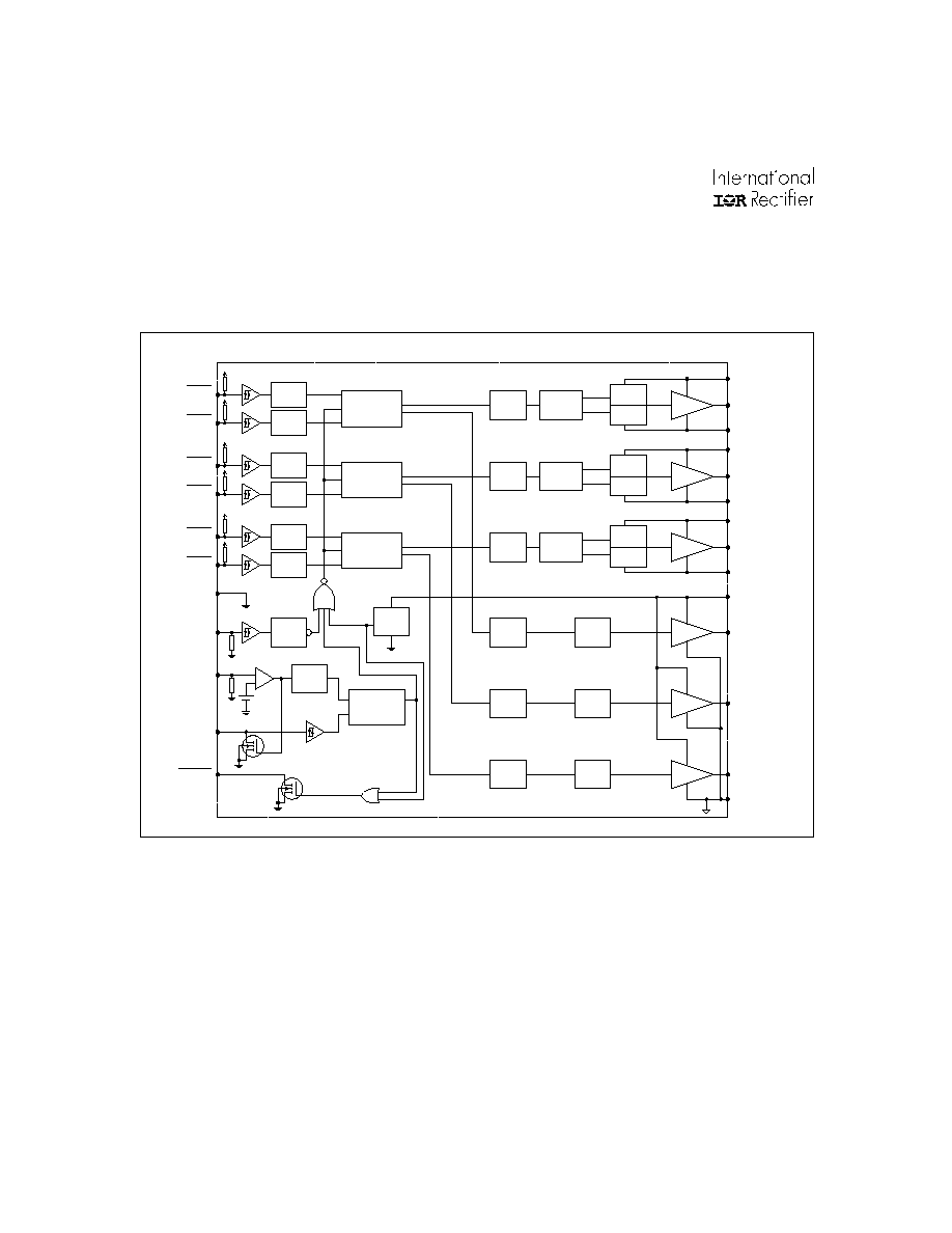
IR21362
COM
VCC
LO1
LO2
LO3
DELAY
VSS/COM
LEVEL
SHIFTER
DELAY
VSS/COM
LEVEL
SHIFTER
DELAY
VSS/COM
LEVEL
SHIFTER
LIN1
HIN1
LIN2
HIN2
LIN3
HIN3
DEADTIME &
SHOOT-THROUGH
PREVENTION
DEADTIME &
SHOOT-THROUGH
PREVENTION
DEADTIME &
SHOOT-THROUGH
PREVENTION
VS1
HO1
VB1
HV
LEVEL
SHIFTER
VSS/COM
LEVEL
SHIFTER
LATCH
UV
DETECT
SET
RESET
DRIVER
VS2
HO2
VB2
HV
LEVEL
SHIFTER
VSS/COM
LEVEL
SHIFTER
LATCH
UV
DETECT
SET
RESET
DRIVER
VS3
HO3
VB3
HV
LEVEL
SHIFTER
VSS/COM
LEVEL
SHIFTER
LATCH
UV
DETECT
SET
RESET
DRIVER
DRIVER
DRIVER
DRIVER
INPUT
NOISE
FILTER
INPUT
NOISE
FILTER
INPUT
NOISE
FILTER
INPUT
NOISE
FILTER
INPUT
NOISE
FILTER
INPUT
NOISE
FILTER
UV
DETECT
EN
ITRIP
+
-
0.5V
RCIN
S
R
Q
FAULT
INPUT
NOISE
FILTER
VSS
INPUT
NOISE
FILTER
SET
DOMINANT
LATCH
Functional Block Diagram
IR2136(2)(3)(5)(6)(7)(8)(J&S) & (PbF)
8
www.irf.com
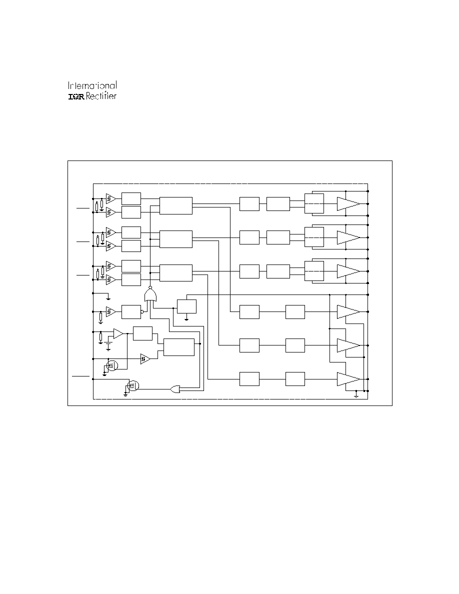
Functional Black Diagram
IR21366/IR21367/IR21368
COM
VCC
LO1
LO2
LO3
DELAY
VSS/COM
LEVEL
SHIFTER
DELAY
VSS/COM
LEVEL
SHIFTER
DELAY
VSS/COM
LEVEL
SHIFTER
LIN1
HIN1
LIN2
HIN2
LIN3
HIN3
DEADTIME &
SHOOT-THROUGH
PREVENTION
DEADTIME &
SHOOT-THROUGH
PREVENTION
DEADTIME &
SHOOT-THROUGH
PREVENTION
VS1
HO1
VB1
HV
LEVEL
SHIFTER
VSS/COM
LEVEL
SHIFTER
LATCH
UV
DETECT
SET
RESET
DRIVER
VS2
HO2
VB2
HV
LEVEL
SHIFTER
VSS/COM
LEVEL
SHIFTER
LATCH
UV
DETECT
SET
RESET
DRIVER
VS3
HO3
VB3
HV
LEVEL
SHIFTER
VSS/COM
LEVEL
SHIFTER
LATCH
UV
DETECT
SET
RESET
DRIVER
DRIVER
DRIVER
DRIVER
UV
DETECT
EN
ITRIP
+
-
RCIN
S
R
Q
FAULT
INPUT
NOISE
FILTER
VSS
INPUT
NOISE
FILTER
SET
DOMINANT
LATCH
www.irf.com
9
IR2136(2)(3)(5)(6)(7)(8)(J&S) & (PbF)
Lead Definitions
Symbol Description
V
CC
Low side and logic fixed supply
VSS
Logic Ground
HIN1,2,3
Logic inputs for high side gate driver outputs (HO1,2,3), out of phase (IR2136/IR21363(5)(6)(7)(8)
HIN1,2,3
Logic inputs for high side gate driver outputs (HO1,2,3), in phase (IR21362)
LIN1,2,3
Logic inputs for low side gate driver outputs (LO1,2,3), out of phase
FAULT
Indicates over-current (ITRIP) or low-side undervoltage lockout has occured. Negative logic,
open-drain output
EN
Logic input to enable I/O functionality. Positive logic, i.e. I/O logic functions when ENABLE is
high. No effect on FAULT and not latched
ITRIP
Analog input for overcurrent shutdown. When active, ITRIP shuts down outputs and activates
FAULT and RCIN low. When ITRIP becomes inactive, FAULT stays active low for an externally
set time T
FLTCLR
, then automatically becomes inactive (open-drain high impedance).
RCIN
External RC network input used to define FAULT CLEAR delay, T
FLTCLR
, approximately equal
to R*C. When RCIN>8V, the FAULT pin goes back into open-drain high-impedance
COM
Low side gate driver return
V
B
1,2,3
High side floating supply
HO1,2,3
High side gate driver outputs
V
S1,2,3
High voltage floating supply returns
LO1,2,3
Low side gate driver output
Note: All input pins and the ITRIP pin are internally clamped with a 5.2V zener diode.
IR2136(2)(3)(5)(6)(7)(8)(J&S) & (PbF)
10
www.irf.com
28 Lead PDIP 44 Lead PLCC w/o 12 leads 28 lead SOIC (wide body)
IR2136/IR21363(5)(6)(7)(8) IR2136/IR21363(5)(6)(7)(8) (J) IR2136/IR21363(5)(6)(7)(8) (S)
Lead Assignments
28 Lead PDIP 44 Lead PLCC w/o 12 leads 28 lead SOIC (wide body)
IR21362 IR21362J
IR21362S
1
VCC
2
HIN1
3
HIN2
4
HIN3
5
LIN1
6
LIN2
7
LIN3
8
FAULT
9
ITRIP
10
EN
11
RCIN
12
VSS
13
COM
14
LO3
28
VB1
27
HO1
26
VS1
25
24
VB2
23
HO2
22
VS2
21
20
VB3
19
HO3
18
VS3
17
16
LO1
15
LO2
1
VCC
2
HIN1
3
HIN2
4
HIN3
5
LIN1
6
LIN2
7
LIN3
8
FAULT
9
ITRIP
10
EN
11
RCIN
12
VSS
13
COM
14
LO3
28
VB1
27
HO1
26
VS1
25
24
VB2
23
HO2
22
VS2
21
20
VB3
19
HO3
18
VS3
17
16
LO1
15
LO2
FAULT
8
9
10
11
LIN1
12
LIN2
13
LIN3
14
15
ITRIP
16
EN
17
7
VSS
LO1
18
LO3
VS3
HO3
VB3
29
41
VS1
LO2
COM
30
31
VS2
HO2
VB2
35
36
37
19
20
21
22
23
24
25
HO1
VB1
VCC
HIN1
HIN2
HIN3
42
43
3
4
5
6
RCIN
FAULT
8
9
10
11
LIN1
12
LIN2
13
LIN3
14
15
ITRIP
16
EN
17
7
VSS
LO1
18
LO3
VS3
HO3
VB3
29
41
VS1
LO2
COM
30
31
VS2
HO2
VB2
35
36
37
19
20
21
22
23
24
25
HO1
VB1
VCC
HIN1
HIN2
HIN3
42
43
3
4
5
6
IR2136
44 LEAD PLCC w/o 12 LEADS
RCIN
1
VCC
2
HIN1
3
HIN2
4
HIN3
5
LIN1
6
LIN2
7
LIN3
8
FAULT
9
ITRIP
10
EN
11
RCIN
12
VSS
13
COM
14
LO3
28
VB1
27
HO1
26
VS1
25
24
VB2
23
HO2
22
VS2
21
20
VB3
19
HO3
18
VS3
17
16
LO1
15
LO2
IR2136
1
VCC
2
HIN1
3
HIN2
4
HIN3
5
LIN1
6
LIN2
7
LIN3
8
FAULT
9
ITRIP
10
EN
11
RCIN
12
VSS
13
COM
14
LO3
28
VB1
27
HO1
26
VS1
25
24
VB2
23
HO2
22
VS2
21
20
VB3
19
HO3
18
VS3
17
16
LO1
15
LO2
IR2136
www.irf.com
11
IR2136(2)(3)(5)(6)(7)(8)(J&S) & (PbF)
Figure 3. Output Enable Timing Waveform
EN
HO1,2,3
LO1,2,3
50%
90%
ten
Figure 1. Input/Output Timing Diagram
HIN1,2,3
LIN1,2,3
EN
ITRIP
FAULT
RCIN
HO1,2,3
LO1,2,3
HIN1,2,3
Figure 2. Switching Time Waveforms
LIN1,2,3
HIN1,2,3
HO1,2,3
LO1,2,3
50%
50%
90%
10%
10%
90%
ton
tr
tf
toff
LIN1,2,3
HIN1,2,3
50%
50%
PW
IN
PW
OUT
IR2136(2)(3)(5)(6)(7)(8)(J&S) & (PbF)
12
www.irf.com
Figure 4. Internal Deadtime Timing Waveforms
LIN1,2,3
HIN1,2,3
HO1,2,3
LO1,2,3
50%
50%
LIN1,2,3
HIN1,2,3
50%
50%
50%
50%
50%
50%
DT
DT
Figure 5. ITRIP/RCIN Timing Waveforms
RCIN
Any
output
tflt
ITRIP
FAULT
50%
50%
titrip
90%
50%
50%
tfltclr
Vrcin,th+
U
t
in,fil
t
in,fil
on
on
on off
off
off
high
low
HIN/LIN
HO/LO
Figure 5.5 Input Filter Function
www.irf.com
13
IR2136(2)(3)(5)(6)(7)(8)(J&S) & (PbF)
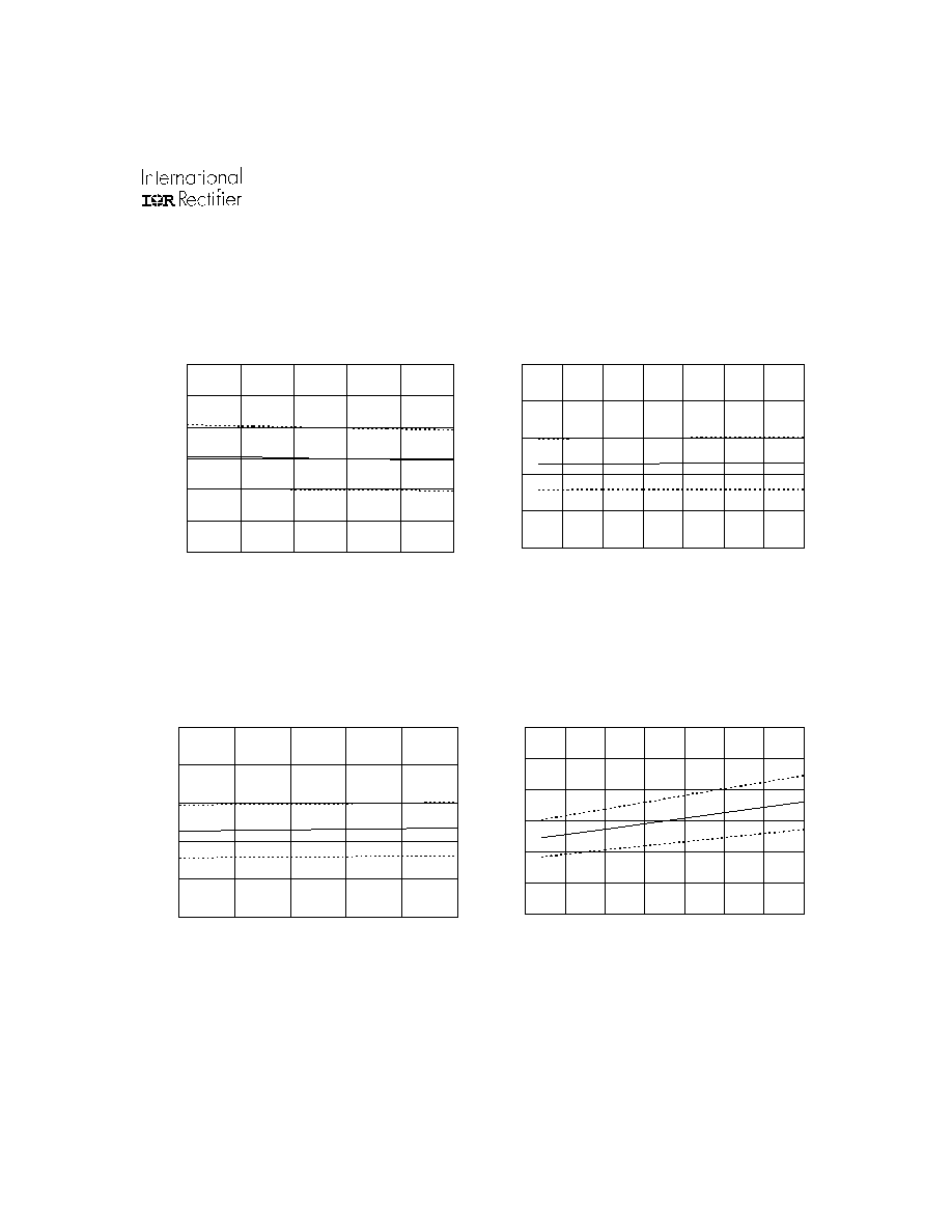
0
200
400
600
800
1000
10
12
14
16
18
20
Supply Voltage (V)
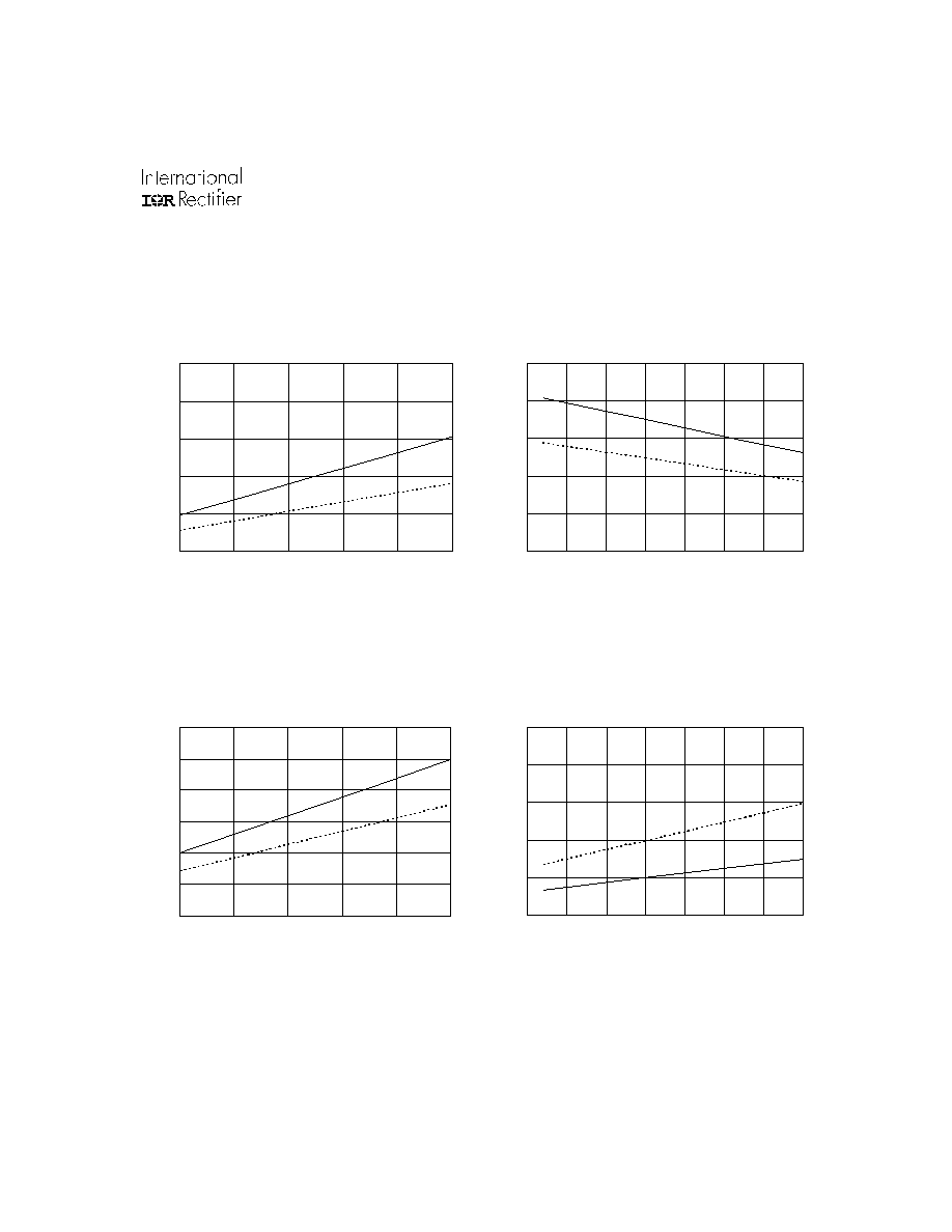
Turn-on Propagation Delay (ns)
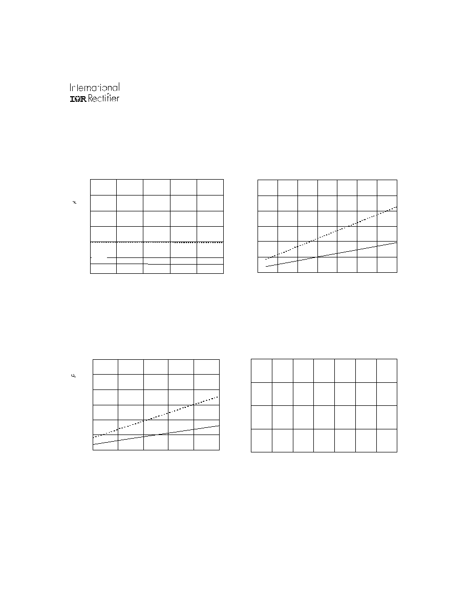
Figure 6B. Turn-on Propagation Delay vs.
Supply Voltage
M i
n.
Typ.
M ax.
0
200
400
600
800
1000
-50
-25
0
25
50
75
100
125
Temperature (
o
C)
Turn-on Propagation Delay (ns)
Typ.
M ax.
Figure 6A. Turn-on Propagation Delay vs.
Temperature
M i
n.
0
200
400
600
800
1000
3
3.5
4
4.5
5
Input Voltage (V)
Turn-on Propagation Delay (ns
)
Figure 6C. Turn-on Propagation Delay vs.
Input Voltage
Typ.
M ax.
M i
n.
0
200
400
600
800
1000
-50
-25
0
25
50
75
100
125
Temperature (
o
C)
Turn-off Propagation Delay (ns)
Typ.
M ax.
Figure 7A. Turn-off Propagation Delay vs.
Temperature
M i
n.
IR2136(2)(3)(5)(6)(7)(8)(J&S) & (PbF)
14
www.irf.com
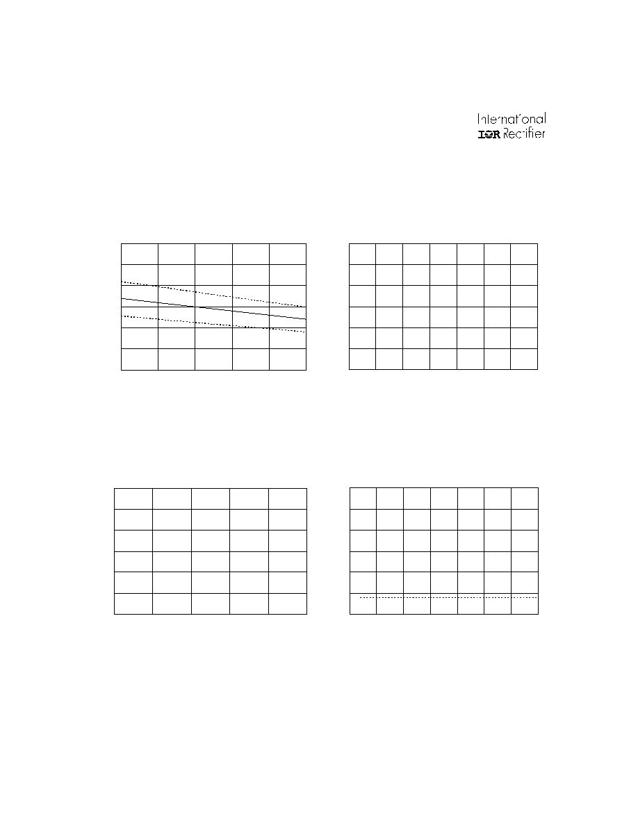
0
200
400
600
800
1000
3
3.5
4
4.5
5
Input Voltage (V)
Turn-off Propagation Delay (ns
)
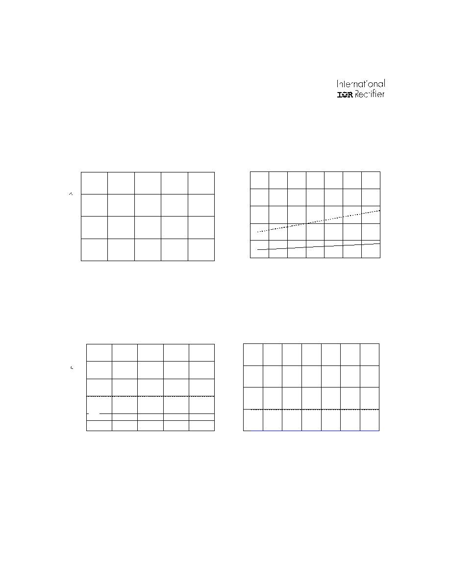
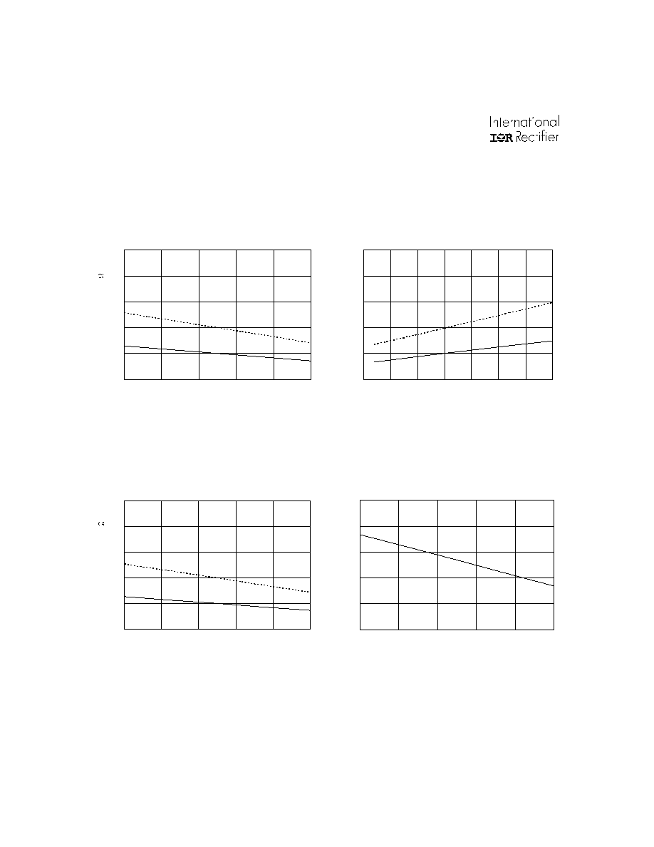
Figure 7C. Turn-off Propagation Delay vs.
Input Voltage
Typ.
M ax.
M i
n.
0
100
200
300
400
-50
-25
0
25
50
75
100
125
Temperature (
o
C)
Turn-on Rise Time (ns
)
Typ.
M ax.
Figure 8A. Turn-on Rise Time vs. Temperature
0
200
400
600
800
1000
10
12
14
16
18
20
Supply Voltage (V)
Turn-off Propagation Delay (ns)
Figure 7B. Turn-off Propagation Delay vs.
Supply Voltage
M in.
Typ.
M ax.
0
100
200
300
400
10
12
14
16
18
20
Supply Voltage (V)
Turn-on Rise Time (ns
)
Figure 8B. Turn-on Rise Time vs. Supply Voltage
Typ.
M ax.
www.irf.com
15
IR2136(2)(3)(5)(6)(7)(8)(J&S) & (PbF)
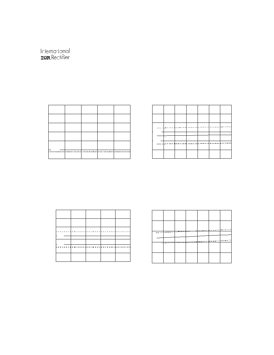
0
50
100
150
200
-50
-25
0
25
50
75
100
125
Temperature (
o
C)
Turn-off Fall Time (ns)
Typ.
M ax.
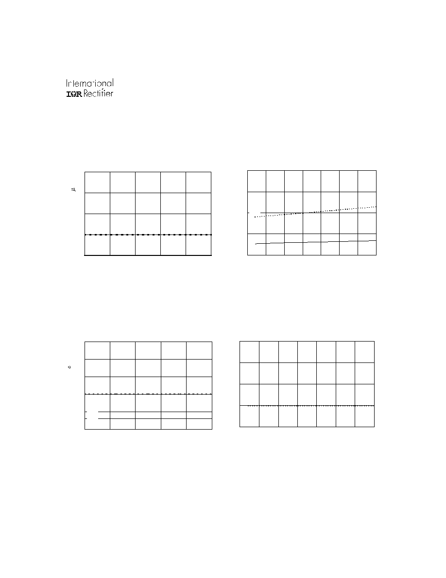
Figure 9A. Turn-off Fall Time vs. Temperature
0
200
400
600
800
1000
-50
-25
0
25
50
75
100
125
Temperature (
o
C)
EN to Output Shutdown Time (ns)
Typ.
M ax.
Figure 10A. EN to Output Shutdown Time
vs. Temperature
M i
n.
0
50
100
150
200
10
12
14
16
18
20
Supply Voltage (V)
Turn-off Fall Time (ns
)
Figure 9B. Turn-off Fall Time vs. Supply Voltage
Typ.
M ax.
0
200
400
600
800
1000
10
12
14
16
18
20
Supply Voltage (V)
EN to Output Shutdown Time (ns)
Figure 10B. EN to Output Shutdown Time vs.
Supply Voltage
Typ.
M ax.
M in.
IR2136(2)(3)(5)(6)(7)(8)(J&S) & (PbF)
16
www.irf.com
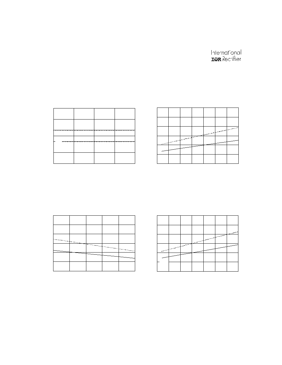
0
300
600
900
1200
1500
-50
-25
0
25
50
75
100
125
Temperature (
o
C)
ITRIP to Output Shutdown Time (ns)
Typ.
M ax.
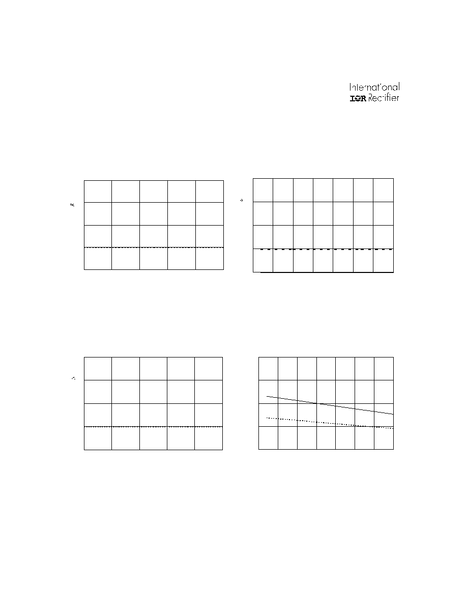
Figure 11A. ITRIP to Output Shutdown Time vs.
Temperature
M i
n.
0
200
400
600
800
1000
3
3.5
4
4.5
5
EN Voltage (V)
EN to Output Shutdown Time (ns)
Figure 10C. EN to Output Shutdown Time
vs. EN Voltage
Typ.
M ax.
M in.
0
300
600
900
1200
1500
10
12
14
16
18
20
Supply Voltage (V)
ITRIP to Output Shutdown Time (ns
)
Figure 11B. ITRIP to Output Shutdown
Time vs. Supply Voltage
Typ.
M ax.
M in.
0
200
400
600
800
1000
1200
-50
-25
0
25
50
75
100
125
Temperature (
o
C)
ITRIP to FAULT Indication Time (ns)
Typ.
M ax.
Figure 12A. ITRIP to FAULT Indication Time vs.
Temperature
M in.
www.irf.com
17
IR2136(2)(3)(5)(6)(7)(8)(J&S) & (PbF)
0
200
400
600
800
1000
1200
10
12
14
16
18
20
Supply Voltage (V)
Fault Indication Time (ns)
Figure 12B. ITRIP to FAULT Indication Time vs.
Supply Voltage
Typ.
M ax.
M i
n.
0.5
1.0
1.5
2.0
2.5
3.0
-50
-25
0
25
50
75
100
125
Temperature (
o
C)
FAULT Clear Time (ms)
Typ.
M ax.
Fig13A. FAULT Clear Time vs. Temperature
M in.
0.5
1.0
1.5
2.0
2.5
3.0
10
12
14
16
18
20
Supply Voltage (V)
Fault Clear Time (ms)
Figure 13B. FAULT Clear Time vs. Supply Voltage
M ax.
M in.
Typ.
0
100
200
300
400
500
600
-50
-25
0
25
50
75
100
125
Temperature (
o
C)
Dead Time (ns)
Typ.
M ax.
Figure 14A. Dead Time vs. Temperature
M in.
IR2136(2)(3)(5)(6)(7)(8)(J&S) & (PbF)
18
www.irf.com
0
100
200
300
400
500
600
10
12
14
16
18
20
Supply Voltage (V)
Dead Time (ns)
Figure 14B. Dead Time Time vs. Supply Voltage
Typ.
M ax.
M i
n.
0
1
2
3
4
5
6
-50
-25
0
25
50
75
100
125
Temperature (
o
C)
Logic "0" Input Threshold (V)
Figure 15A. Logic "0" Input Threshold vs.
Temperature
M ax.
0
1
2
3
4
5
6
10
12
14
16
18
20
Supply Voltage (V)
Logic "0" Input Threshold (V)
Figure 15B. Logic "0" Input Threshold vs.
Supply Voltage
M ax.
0
1
2
3
4
5
6
-50
-25
0
25
50
75
100
125
Temperature (
o
C)
Logic "1" Input Threshold (V)
M i
n.
Figure 16A. Logic "1" Input Threshold vs.
Temperature
www.irf.com
19
IR2136(2)(3)(5)(6)(7)(8)(J&S) & (PbF)
0
1
2
3
4
5
6
10
12
14
16
18
20
Supply Voltage (V)
Logic "1" Input Threshold (V)
Figure 16B. Logic "1" Input Threshold vs.
Supply Voltage
M i
n.
200
300
400
500
600
700
800
-50
-25
0
25
50
75
100
125
Temperature (
o
C)
ITRIP Positive Going Threshold (m
V
Typ.
M ax.
Figure 17A. ITRIP Positive Going Threshold vs.
Temperature (IR2136/21362/21363/IR21366 Only)
M in.
200
300
400
500
600
700
800
10
12
14
16
18
20
Supply Voltage (V)
ITRIP Positive Going Threshold (m
V
Figure 17B. ITRIP Positive Going Threshold vs.
Supply Voltage (IR2136/21362/21363/IR21366 Only)
Typ.
M ax.
M in.
3.0
3.5
4.0
4.5
5.0
5.5
-50
-25
0
25
50
75
100
125
Temperature (
o
C)
ITRIP Positive Going Threshold (
V
Typ.
M ax.
Figure 17C. ITRIP Positive Going Threshold vs.
Temperature (IR21365/IR21367/IR21368 Only)
M in.
IR2136(2)(3)(5)(6)(7)(8)(J&S) & (PbF)
20
www.irf.com
0.0
0.5
1.0
1.5
2.0
2.5
3.0
-50
-25
0
25
50
75
100
125
Temperature (
o
C)
High Level Output Voltage (V)
Typ.
M ax.
Figure 18A. High Level Output vs. Temperature
0.0
0.5
1.0
1.5
2.0
2.5
3.0
10
12
14
16
18
20
Supply Voltage (V)
High Level Output Voltage (V)
Figure 18B. High Level Output vs. Supply Voltage
Typ.
M ax.
0.0
0.2
0.4
0.6
0.8
1.0
1.2
-50
-25
0
25
50
75
100
125
Temperature (
o
C)
Low Level Output Voltage (V)
Typ.
M ax.
Figure 19A. Low Level Output vs. Temperature
3.0
3.5
4.0
4.5
5.0
5.5
12
14
16
18
20
Supply Voltage (V)
ITRIP Positive Going Threshold (
V
Figure 17D. ITRIP Positive Going Threshold vs.
Supply Voltage (IR21365/IR21367/IR21368 Only)
Typ.
M ax.
M in.
www.irf.com
21
IR2136(2)(3)(5)(6)(7)(8)(J&S) & (PbF)
0.0
0.2
0.4
0.6
0.8
1.0
1.2
10
12
14
16
18
20
Supply Voltage (V)
Low Level Output Voltage (V)
Figure 19B. Low Level Output vs. Supply Voltage
Typ.
M ax.
8
9
10
11
12
13
-50
-25
0
25
50
75
100
125
Temperature (
o
C)
V
CC
or V
BS
Undervoltage Lockout (+) (V)
Typ.
M ax.
Figure 22. V
CC
or V
BS
Undervoltage (+) vs.
Temperature (IR21362 Only)
M i
n.
7
8
9
10
11
12
-50
-25
0
25
50
75
100
125
Temperature (
o
C)
V
CC
or V
BS
Undervoltage Lockout (+) (
V
Typ.
M ax.
Figure 20. V
CC
or V
BS
Undervoltage (+)
vs. Temperature (IR2136/IR21368 Only)
M in.
6
7
8
9
10
11
-50
-25
0
25
50
75
100
125
Temperature (
o
C)
V
CC
or V
BS
Undervoltage Lockout (-) (V)
Typ.
M ax.
Figure 21. V
CC
or V
BS
Undervoltage (-)
vs. Temperature (IR2136/IR21368 Only)
M in.
IR2136(2)(3)(5)(6)(7)(8)(J&S) & (PbF)
22
www.irf.com
7
8
9
10
11
12
-50
-25
0
25
50
75
100
125
Temperature (
o
C)
V
CC
or V
BS
Undervoltage Lockout (-) (V
)
Typ.
M ax.
Figure 23. V
CC
or V
BS
Undervoltage (-) vs.
Temperature (IR21362 Only)
M in.
0
100
200
300
400
500
-50
-25
0
25
50
75
100
125
Temperature (
o
C)
Offset Supply Leakage Current (
µ
A)
M ax.
Figure 26A. Offset Supply Leakage Current vs.
Temperature
10
11
12
13
-50
-25
0
25
50
75
100
125
Temperature (
o
C)
V
CC
or V
BS
Undervoltage Lockout (+) (V)
Typ.
M ax.
Figure 24. V
CC
or V
BS
Undervoltage (+) vs.
Temperature (IR21363/21365/IR21366/IR21367 Only)
M in.
9
10
11
12
13
-50
-25
0
25
50
75
100
125
Temperature (
o
C)
V
CC
or V
BS
Undervoltage Lockout (-) (V)
Figure 25. V
CC
or V
BS
Undervoltage (-) vs.
Temperature (IR21363/21365/IR21366/IR21367 Only)
M in.
Typ.
M ax.
www.irf.com
23
IR2136(2)(3)(5)(6)(7)(8)(J&S) & (PbF)
0
100
200
300
400
500
100
200
300
400
500
600
V
B
Boost Voltage (V)
Offset Supply Leakage Current (
A)
Figure 26B. Offset Supply Leakage Current vs.
V
B
Boost Voltage
M ax.
0
50
100
150
200
250
-50
-25
0
25
50
75
100
125
Temperature (
o
C)
V
BS
Supply Current (
µ
A)
Typ.
M ax.
Figure 27A. V
BS
Supply Current vs. Temperature
0
50
100
150
200
250
10
12
14
16
18
20
V
BS
Floating Supply Voltage (V)
V
BS
Supply Current (
A)
Figure 27B. V
BS
Supply Current vs.
V
BS
Floating Supply Voltage
Typ.
M ax.
0
1
2
3
4
5
-50
-25
0
25
50
75
100
125
Temperature (
o
C)
V
CC
Supply Current (mA)
Typ.
M ax.
Figure 28A. V
CC
Supply Current vs. Temperature
IR2136(2)(3)(5)(6)(7)(8)(J&S) & (PbF)
24
www.irf.com
0
1
2
3
4
5
10
12
14
16
18
20
Supply Voltage (V)
V
CC
Supply Current (mA)
Figure 28B. V
CC
Supply Current vs.
V
CC
Supply Voltage
Typ.
M ax.
0
200
400
600
800
-50
-25
0
25
50
75
100
125
Temperature (
o
C)
Logic "1" Input Current (
µ
A)
Typ.
M ax.
Figure 29A. Logic "1" Input Current vs. Temperature
(IR2136/21363/21365 and IR21362 Low Side Only)
0
50
100
150
200
250
300
-50
-25
0
25
50
75
100
125
Temperature (
o
C)
Logic "1" Input Current (
µ
A)
Typ.
M ax.
Figure 29C. Logic "1" Input Current vs.
Temperature (IR21362 High Side Only)
0
200
400
600
800
10
12
14
16
18
20
Supply Voltage (V)
Logic "1" Input Current (
A)
Typ.
M ax.
Figure 29B. Logic "1" Input Current vs. Supply Voltage
(IR2136/21363/21365 and IR21362 Low Side Only)
www.irf.com
25
IR2136(2)(3)(5)(6)(7)(8)(J&S) & (PbF)
0
50
100
150
200
250
300
10
12
14
16
18
20
Supply Voltage (V)
Logic "1" Input Current (
A)
Figure 29D. Logic "1" Input Current vs.
Supply Voltage (IR21362 High Side Only)
Typ.
M ax.
0
100
200
300
400
500
600
-50
-25
0
25
50
75
100
125
Temperature (
o
C)
Logic "0" Input Current (
µ
A)
Typ.
M ax.
Figure 30A. Logic "0" Input Current vs. Temperature
(IR2136/21363/21365 and IR21362 Low Side Only)
0
1
2
3
4
-50
-25
0
25
50
75
100
125
Temperature (
o
C)
Logic "0" Input Current (
µ
A)
Typ.
M ax.
Figure 30C. Logic "0" Input Current vs.
Temperature (IR21362 High Side Only)
0
100
200
300
400
500
600
10
12
14
16
18
20
Supply Voltage (V)
Logic "0" Input Current (
A)
Figure 30B. Logic "0" Input Current vs. Supply
Voltage (IR2136/21363/21365 and IR21362 Low Side
Typ.
M ax.
Only)
IR2136(2)(3)(5)(6)(7)(8)(J&S) & (PbF)
26
www.irf.com
0
1
2
3
4
10
12
14
16
18
20
Supply Voltage (V)
Logic "0" Input Current (
A)
Figure 30D. Logic "0" Input Current vs.
Supply Voltage (IR21362 High Side Only)
Typ.
M ax.
0
50
100
150
200
250
-50
-25
0
25
50
75
100
125
Temperature (
o
C)
"High" ITRIP Current (
µ
A)
Typ.
M ax.
Figure 31A. "High" ITRIP Current vs. Temperature
0
50
100
150
200
250
10
12
14
16
18
20
Supply Voltage (V)
"High" ITRIP Current (
A)
Figure 31B. "High" ITRIP Current vs. Supply Voltage
Typ.
M ax.
0
1
2
3
4
-50
-25
0
25
50
75
100
125
Temperature (
o
C)
"Low" ITRIP Current (
µ
A)
M ax.
Figure 32A. "Low" ITRIP Current vs. Temperature
Typ.
www.irf.com
27
IR2136(2)(3)(5)(6)(7)(8)(J&S) & (PbF)
0
1
2
3
4
10
12
14
16
18
20
Supply Voltage (V)
"Low" ITRIP Current (
A)
Figure 32B. "Low" ITRIP Current vs. Supply Voltage
Typ.
M ax.
0
50
100
150
200
-50
-25
0
25
50
75
100
125
Temperature (
o
C)
"High" IEN Current (
µ
A)
M ax.
Figure 33A. "High" IEN Current vs. Temperature
Typ.
0
50
100
150
200
250
10
12
14
16
18
20
Supply Voltage (V)
"High" IEN Current (
A)
Figure 33B. "High" IEN Current vs. Supply Voltage
Typ.
M ax.
0
1
2
3
4
-50
-25
0
25
50
75
100
125
Temperature (
o
C)
"Low" IEN Current (
µ
A)
Typ.
M ax.
Figure 34A. "Low" IEN Current vs. Temperature
IR2136(2)(3)(5)(6)(7)(8)(J&S) & (PbF)
28
www.irf.com
0
1
2
3
4
-50
-25
0
25
50
75
100
125
Temperature (
o
C)
RCIN Input Bias Current (
A)
M ax.
Figure 35A. RCIN Input Bias Current
vs. Temperature
Typ.
0
1
2
3
4
10
12
14
16
18
20
Supply Voltage (V)
RCIN Input Bias Current (
A)
Figure 35B. RCIN Input Bias Current vs.
Supply Voltage
Typ.
M ax.
0
100
200
300
400
-50
-25
0
25
50
75
100
125
Temperature (
o
C)
Output Source Current (mA)
Typ.
Figure 36A. Output Source Current vs.
Temperature
M in.
Figure 34B. "Low" IEN Current vs. Supply Voltage
0
1
2
3
4
10
12
14
16
18
20
Supply Voltage (V)
"Low" IEN Current (
A)
Figure 34B. "Low" IEN Current vs. Supply Voltage
Typ.
M ax.
www.irf.com
29
IR2136(2)(3)(5)(6)(7)(8)(J&S) & (PbF)
0
100
200
300
400
500
10
12
14
16
18
20
Supply Voltage (V)
Output Source Current (mA)
Figure 36B. Output Source Current vs.
Supply Voltage
Typ.
M i
n.
0
100
200
300
400
500
-50
-25
0
25
50
75
100
125
Temperature (
o
C)
Output Sink Current (mA)
Typ.
Figure 37A. Output Sink Current vs.
Temperature
M i
n.
0
100
200
300
400
500
600
10
12
14
16
18
20
Supply Voltage (V)
Output Sink Current (mA)
Figure 37B. Output Sink Current vs.
Supply Voltage
Typ.
M i
n.
0
50
100
150
200
250
-50
-25
0
25
50
75
100
125
Temperature (
o
C)
RCIN Low On-resistance (
)
Typ.
M ax.
Figure 38A. RCIN Low On-resistance vs.
Temperature
IR2136(2)(3)(5)(6)(7)(8)(J&S) & (PbF)
30
www.irf.com
0
50
100
150
200
250
10
12
14
16
18
20
Supply Voltage (V)
RCIN Low On-resistance (
)
Figure 38B. RCIN Low On-resistance vs.
Supply Voltage
Typ.
M ax.
0
50
100
150
200
250
-50
-25
0
25
50
75
100
125
Temperature (
o
C)
FAULT Low On-resistance (
)
Typ.
M ax.
Figure 39A. FAULT Low On-resistance vs.
Temperature
0
50
100
150
200
250
10
12
14
16
18
20
Supply Voltage (V)
FAULT Low On-resistance (
)
Figure 39B. FAULT Low On-resistance vs.
Supply Voltage
Typ.
M ax.
-15
-12
-9
-6
-3
0
10
12
14
16
18
20
Supply Voltage (V)
V
S
Offset Supply Voltage (V)
Figure 40. Maximum V
S
Negative Offset vs. V
BS
Supply Voltage
Typ.
www.irf.com
31
IR2136(2)(3)(5)(6)(7)(8)(J&S) & (PbF)
20
40
60
80
100
120
0.1
1
10
100
Frequency (KHz)
Junction Temperature (
o
C)
100V
200V
300V
0V
20
40
60
80
100
120
0.1
1
10
100
Frequency (KHz)
Junction Temperature (
o
C)
100
V
200V
300V
0V
20
40
60
80
100
120
0.1
1
10
100
Frequency (KHz)
Junction Temperature (
o
C)
100
V
200V
300V
0V
20
40
60
80
100
120
0.1
1
10
100
Frequency (KHz)
Junction Temperature (
o
C)
100
V
200V
300V
0V
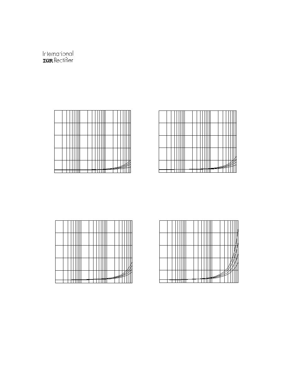
Figure 42. IR2136/IR21362(3)(5)(6)(7)(8)
vs. Frequency (IRG4BC30W), Rgate=15
, Vcc=15V
Figure 41. IR2136/IR21362(3)(5)(6)(7)(8)
vs. Frequency (IRG4BC20W), Rgate=33
, Vcc=15V
Figure 44. IR2136/IR21362(3)(5)(6)(7)(8)
vs. Frequency (IRG4PC50W), Rgate=5
, Vcc=15V
Figure 43. IR2136/IR21362(3)(5)(6)(7)(8)
vs. Frequency (IRG4BC40W), Rgate=10
, Vcc=15V
IR2136(2)(3)(5)(6)(7)(8)(J&S) & (PbF)
32
www.irf.com
20
40
60
80
100
120
0.1
1
10
100
Frequency (KHz)
Junction Temperature (
o
C)
100V
200V
300V
0V
20
40
60
80
100
120
0.1
1
10
100
Frequency (KHz)
Junction Temperature (
o
C)
100V
200V
300V
0V
20
40
60
80
100
120
0.1
1
10
100
Frequency (KHz)
Junction Temperature (
o
C)
100V
200V
300V
0V
20
40
60
80
100
120
0.1
1
10
100
Frequency (KHz)
Junction Temperature (
o
C)
100V
200V
300V
0V
Figure 46. IR2136/IR21362(3)(5)(6)(7)(8) (J)
vs. Frequency (IRG4BC30W), Rgate=15
, Vcc=15V
Figure 45. IR2136/IR21362(3)(5)(6)(7)(8) (J)
vs. Frequency (IRG4BC20W), Rgate=33
, Vcc=15V
Figure 48. IR2136/IR21362(3)(5)(6)(7)(8) (J)
vs. Frequency (IRG4PC50W), Rgate=5
, Vcc=15V
Figure 47. IR2136/IR21362(3)(5)(6)(7)(8) (J)
vs. Frequency (IRG4BC40W), Rgate=10
, Vcc=15V
www.irf.com
33
IR2136(2)(3)(5)(6)(7)(8)(J&S) & (PbF)
20
40
60
80
100
120
0.1
1
10
100
Frequency (KHz)
Junction Temperature (
o
C)
100
V
200V
300V
0V
20
40
60
80
100
120
0.1
1
10
100
Frequency (KHz)
Junction Temperature (
o
C)
100
V
200V
300V
0V
20
40
60
80
100
120
0.1
1
10
100
Frequency (KHz)
Junction Temperature (
o
C)
100
V
200V
300V
0V
20
40
60
80
100
120
0.1
1
10
100
Frequency (KHz)
J
u
nc
t
i
on
T
e
m
p
erat
ure
(
o
C)
100
V
200V
300V
0V
Figure 50. IR2136/IR21362(3)(5)(6)(7)(8) (S)
vs. Frequency (IRG4BC30W), Rgate=15
, Vcc=15V
Figure 49. IR2136/IR21362(3)(5)(6)(7)(8) (S)
vs. Frequency (IRG4BC20W), Rgate=33
, Vcc=15V
Figure 52. IR2136/IR21362(3)(5)(6)(7)(8) (S)
vs. Frequency (IRG4PC50W), Rgate=5
, Vcc=15V
Figure 51. IR2136/IR21362(3)(5)(6)(7)(8) (S)
vs. Frequency (IRG4BC40W), Rgate=10
, Vcc=15V
IR2136(2)(3)(5)(6)(7)(8)(J&S) & (PbF)
34
www.irf.com
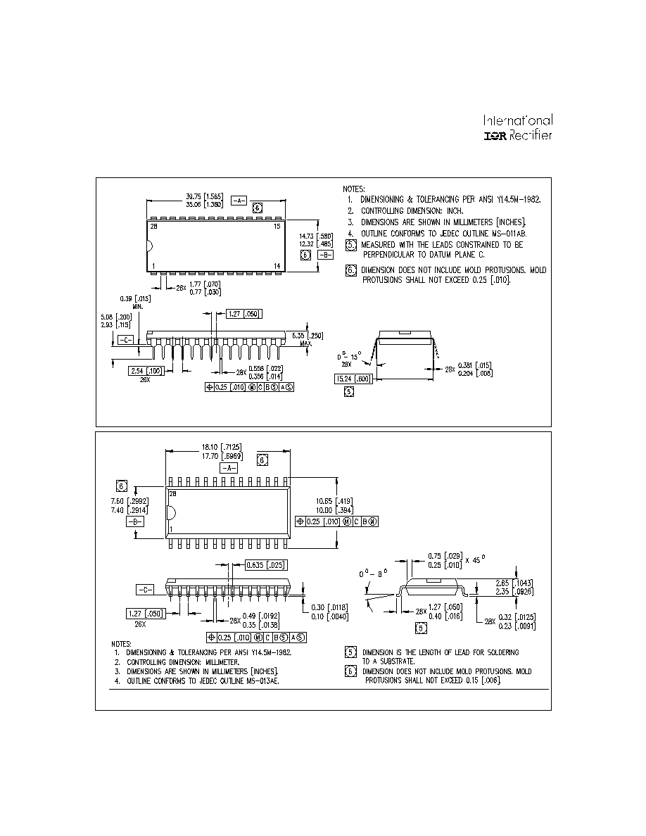
28-Lead PDIP (wide body)
01-6011
01-3024 02
(MS-011AB)
Case outlines
01-6013
01-3040 02
(MS-013AE)
28-Lead SOIC (wide body)
www.irf.com
35
IR2136(2)(3)(5)(6)(7)(8)(J&S) & (PbF)
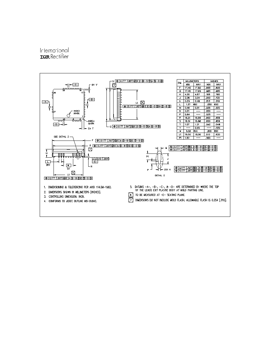
01-6009 00
01-3004 02(mod.
) (MS-018AC)
44-Lead PLCC w/o 12 leads
NOTES
IR2136(2)(3)(5)(6)(7)(8)(J&S) & (PbF)
36
www.irf.com
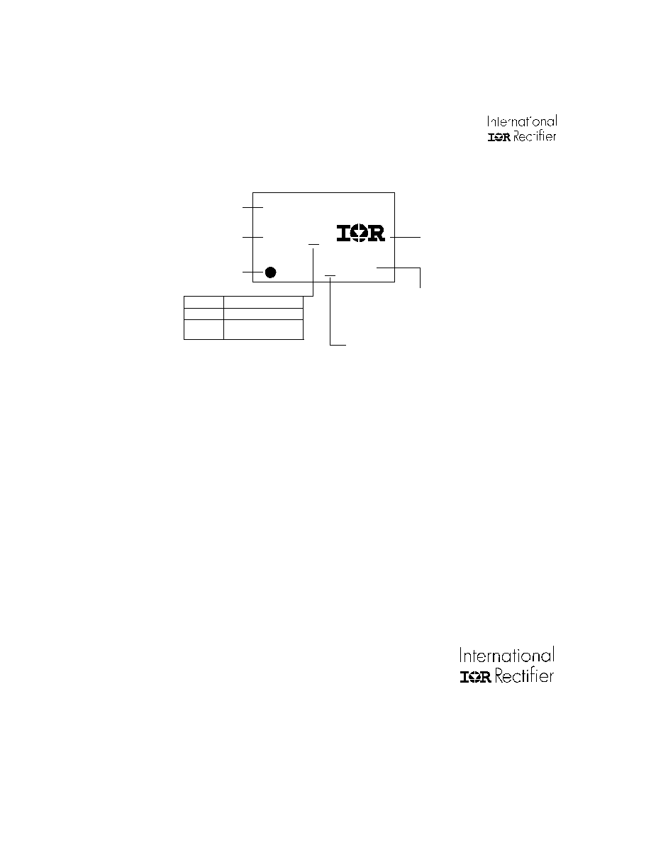
LEADFREE PART MARKING INFORMATION
Lead Free Released
Non-Lead Free
Released
Part number
Date code
IRxxxxxx
YWW?
?XXXX
Pin 1
Identifier
IR logo
Lot Code
(Prod mode - 4 digit SPN code)
Assembly site code
Per SCOP 200-002
P
?
MARKING CODE
ORDER INFORMATION
Basic Part
28-Lead PDIP IR2136/IR21363(5)(6)(7)(8)
order IR2136/IR21363(5)(6)(7)(8)
28-Lead SOIC IR2136/IR21363(5)(6)(7)(8) (S)
order IR2136/IR21363(5)(6)(7)(8) (S)
44-Lead PLCC IR2136/IR21363(5)(6)(7)(8) (J)) order IR2136/IR21363(5)(6)(7)(8) (J)
28-Lead PDIP IR21362
order IR21362
28-Lead SOIC IR21362S
order IR21362S
44-Lead PLCC IR21362J
order IR21362J
Leadfree Part
28-Lead PDIP IR2136/IR21363(5)(6)(7)(8)
order IR2136/IR21363(5)(6)(7)(8)PbF
28-Lead SOIC IR2136/IR21363(5)(6)(7)(8) (S)
order IR2136/IR21363(5)(6)(7)(8) (S)PbF
44-Lead PLCC IR2136/IR21363(5)(6)(7)(8) (J)) order IR2136/IR21363(5)(6)(7)(8) (J)PbF
28-Lead PDIP IR21362
order IR21362PbF
28-Lead SOIC IR21362S
order IR21362SPbF
44-Lead PLCC IR21362J
order IR21362JPbF
WORLD HEADQUARTERS: 233 Kansas Street, El Segundo, California 90245 Tel: (310) 252-7105
This product has been qualified per industrial level
http://www.irf.com/ Data and specifications subject to change without notice. 4/13/2004