 | ÐлекÑÑоннÑй компоненÑ: IR2171 | СкаÑаÑÑ:  PDF PDF  ZIP ZIP |
Äîêóìåíòàöèÿ è îïèñàíèÿ www.docs.chipfind.ru
ADVANCE INFORMATION Data Sheet No. PD60175-C
IR2171
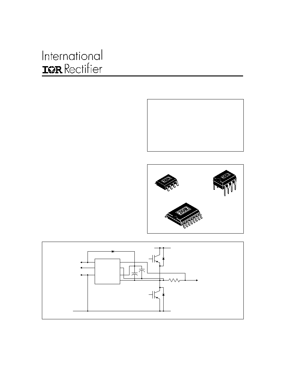
Block Diagram
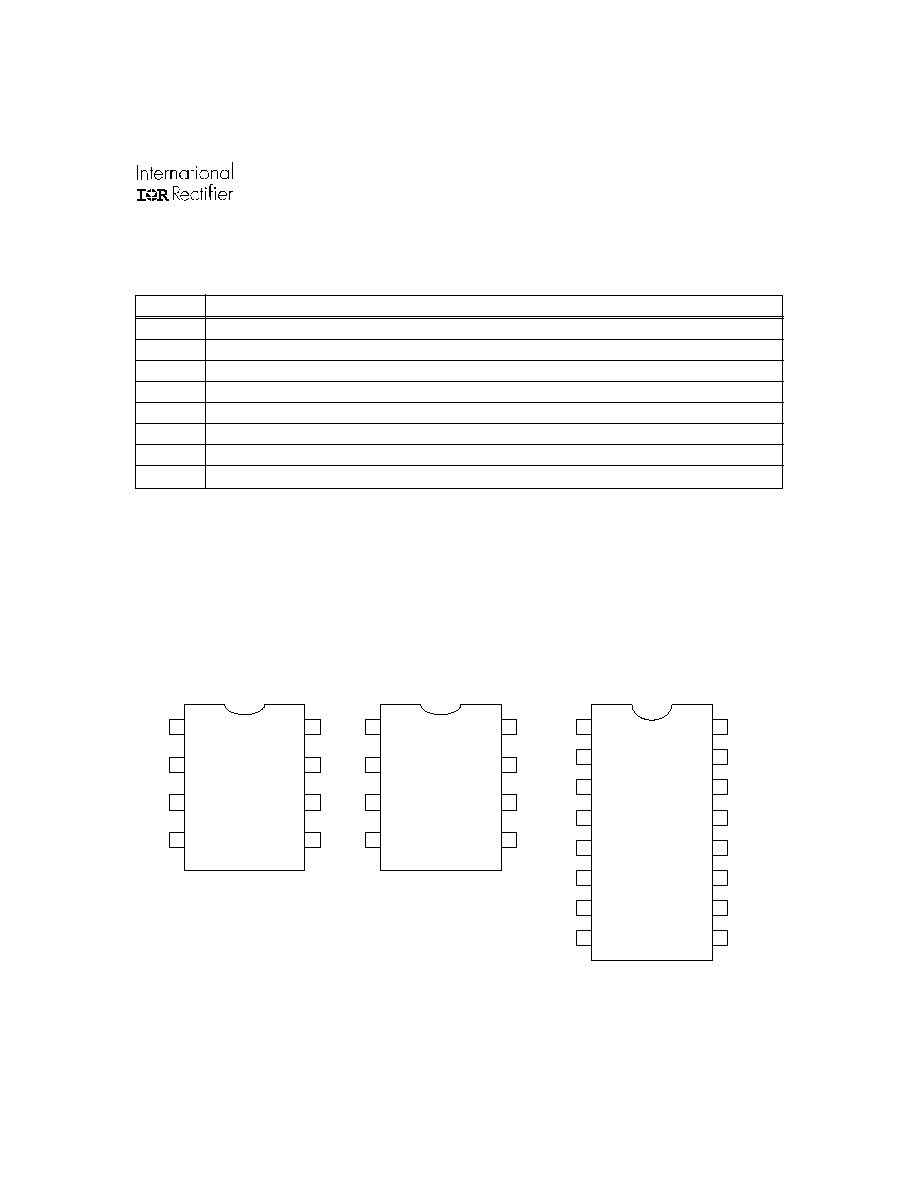
Packages
Product Summary
V
OFFSET
600V
I
QBS
1mA
V
in
+/-260mVmax
Gain temp. drift 20ppm/
o
C(typ.)
fo
40kHz (typ.)
LINEAR CURRENT SENSING IC
Features
·
Floating channel up to +600V
·
Monolithic integration
·
Linear current feedback through shunt resistor
·
Direct digital PWM output for easy interface
·
Low IQBS allows the boot strap power supply
·
High Common Mode Noise Immunity
·
Input overvoltage Protection for IGBT short circuit
condition
·
Open Drain output
Descriptions
IR2171 is the linear current sensing IC designed for
motor drive applications. It senses the motor phase
current through an extenal shunt resistor, converts
from analog to digital signal, and transfers the signal
to the low side. IR's proprietary high voltage isolation
technology is implemented to enable the high band-
width signal processing. The output format is discrete
PWM at 40kHz to eliminate need for the A/D input
interface. It allows direct interface to uP via simple
counter based measurement. The independently pow-
ered output enables easy interface to the opto cou-
pler device for galvanic isolation if needed.
8 Lead SOIC
16 Lead SOIC
(wide body)
8 Lead PDIP
V B
V+
V-
V S
V C C
P O
C O M
IR2171
G N D
1 5 V
To Motor Phase
P W M O u t p u t
Up to 600V
N C
2
IR2171
ADVANCE INFORMATION
www.irf.com
Symbol Definition
Min.
Max.
Units
V
S
High side offset voltage
-0.3
600
V
BS
High side floating supply voltage
V
S
-0.3
25
V
CC
Low side and logic fixed supply voltage
-0.3
25
V
IN
Maximum input voltage between V
IN+
and
V
IN-
-5
5
V
PO
Digital PWM output voltage
COM -0.3
V
CC
+0.3
V
IN-
V
IN-
input voltage
(note 1)
Vs -5
V
B
+0.3
dV/dt
Allowable offset voltage slew rate
--
50
V/ns
P
D
Package power dissipation @ T
A
+25°C
8 lead SOIC
--
.625
8 lead PDIP
--
1.0
16 lead SOIC
--
1.25
Rth
JA
Thermal resistance, junction to ambient
8 lead SOIC
--
200
8 lead PDIP
--
125
16 lead SOIC
--
100
T
J
Junction temperature
--
150
T
S
Storage temperature
-55
150
T
L
Lead temperature (soldering, 10 seconds)
--
300
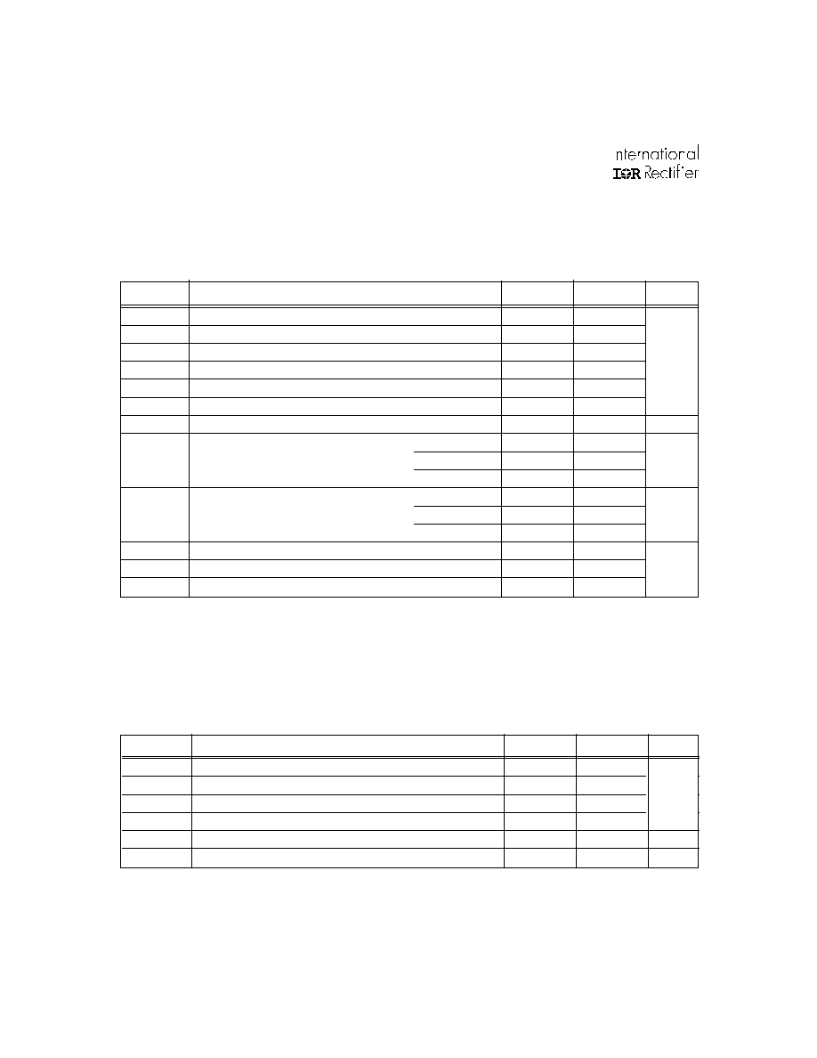
Absolute Maximum Ratings
Absolute maximum ratings indicate sustained limits beyond which damage to the device may occur. All voltage param-
eters are absolute voltages referenced to COM, all currents are defined positive into any lead. The thermal resistance
and power dissipation ratings are measured under board mounted and still air conditions.
V
°C/W
Recommended Operating Conditions
The output logic timing diagram is shown in figure 1. For proper operation the device should be used within the recom-
mended conditions.
W
°C
Symbol Definition
Min.
Max.
Units
V
B
High side floating supply voltage
V
S
+13.0
V
S
+20
V
S
High side floating supply offset voltage
note 2
600
V
PO
Digital PWM output voltage
COM
V
CC
V
CC
Low side and logic fixed supply voltage
9.5
20
V
IN
Input voltage between V
IN+
and V
IN-
-260
+260
mV
T
A
Ambient temperature
-40
125
°C
V
Note 2: Logic operation for Vs of -5 to +600V. Logic state held for Vs of -5V to -V
BS
.
Note 1: Capacitors are required between V
B
and Vin-, and between V
B
and Vs pins when bootstrap power
is used. The external power supply, when used, is required between V
B
and Vin-, and between V
B
and Vs
pins.
3
IR2171
ADVANCE INFORMATION
www.irf.com
Symbol
Definition
Min.
Typ. Max. Units Test Conditions
Propagation delay characteristics
fo
Carrier frequency output
--
40
--
kHz
f
/
T
A
Temperature drift of carrier frequency
--
500
--
ppm/
o
C
Dmin
Minimum duty
--
7
--
%
Dmax
Maximum duty
--
93
--
%
BW
fo bandwidth
15
kHz
PHS
Phase shift at 1kHz
-10
o
AC Electrical Characteristics
V
CC
= V
BS
= 15V, unless otherwise specified.
V
IN
Nominal input voltage range before saturation
-260
--
260
|V
IN+ _
V
IN-
|
V
OS
Input offset voltage
-10
0
10
V
IN
= 0V (Note 1)
V
OS
/
T
A
Input offset voltage temperature drift
--
25
--
µV/
o
C
G
Gain (duty cycle % per V
IN
)
157
162
167
%/V
max gain error=5%
(Note 2)
G
/
T
A
Gain temperature drift
--
20
--
ppm/
o
C
I
LK
Offset supply leakage current
--
--
50
µA
V
B
= V
S
= 600V
I
QBS
Quiescent V
BS
supply current
--
1
2
V
S
= 0V
I
QCC
Quiescent V
CC
supply current
--
--
1
LIN
Linearity (duty cycle deviation from ideal linearity
--
0.5
1
%
curve)
LIN
/
T
A
Linearity temperature drift
--
.005
--
%/
o
C
I
O-
Output sink current
20
--
--
mA
2
--
--
DC Electrical Characteristics
V
CC
= V
BS
= 15V, unless otherwise specified.
figure 1
V
IN
= 0V & 5V
VIN+=-260mV,VIN-=0
VIN+=+260mV,VIN-=0
Symbol
Definition
Min.
Typ. Max. Units Test Conditions
mV
V
O
= 1V
V
O
= 0.1V
Note 1:
±10mV offset represents ±1.5% duty cycle fluctuation
Note 2: Gain = (full range of duty cycle in %) / (full input voltage range).
V
IN
+=100mV pk-pk
sine wave, -3dB
V
IN
+=100mVpkpk
sine wave
mA
4
IR2171
ADVANCE INFORMATION
www.irf.com
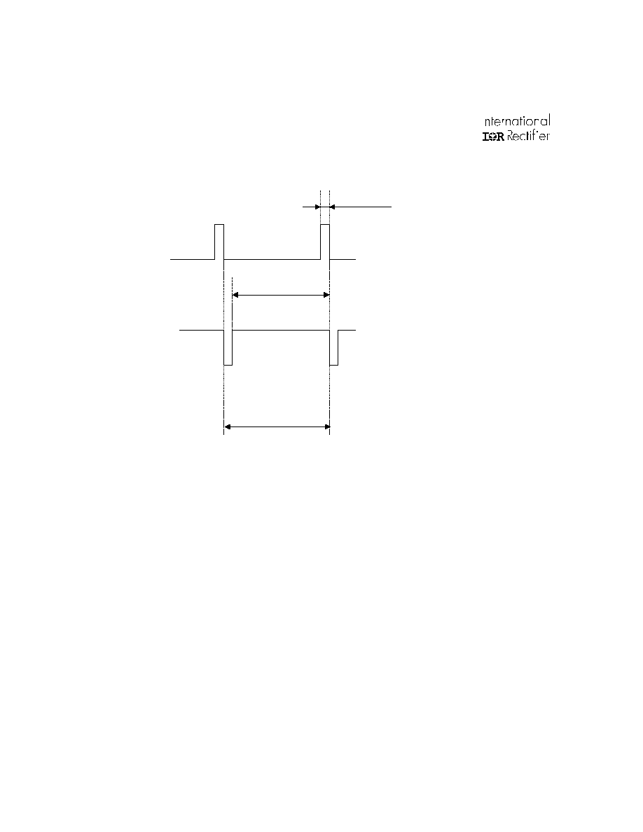
Application Hint:
Temperature drift of the output carrier frequency can be cancelled by measuring both a PWM period and
the on-time of PWM (Duty) at a same time. Since both periods vary in the same direction, computing the
ratio between these values at each PWM periods gives consistent measurement of the current feedback
over the temperature drift.
Vin+= -260mV
Vin- = 0V
Vin+= +260mV
Vin- = 0V
Duty=93%
Duty=7%
Carrier Frequency =
40kHz
PO
PO
Timing Waveforms
Figure 1 Output waveform
5
IR2171
ADVANCE INFORMATION
www.irf.com
Lead Assignment
Lead Definitions
Symbol Description
V
CC
Low side and logic supply voltage
COM
Low side logic ground
VIN+
Positive sense input
VIN-
Negative sense input
VB
High side supply
VS
High side return
PO
Digital PWM output
N.C.
No connection
IR2171S
8
7
6
4
3
2
1
V C C
N C
P O
C O M
V S
VIN-
VIN+
V B
5
8 l e a d S O I C
IR2171
8
7
6
4
3
2
1
V C C
N C
P O
C O M
V S
VIN-
VIN+
V B
5
8 l e a d P D I P
IR21716S
1 6
1 5
1 4
4
3
2
1
V C C
N C
P O
C O M
V S
VIN-
VIN+
V B
1 3
1 6 l e a d S O I C
5
7
6
8
1 2
1 1
1 0
9
N C
N C
N C
N C
N C
N C
N C
N C