 | ÐлекÑÑоннÑй компоненÑ: IR51H224 | СкаÑаÑÑ:  PDF PDF  ZIP ZIP |
Äîêóìåíòàöèÿ è îïèñàíèÿ www.docs.chipfind.ru
Preliminary Data Sheet No. PD60083
I
Features
··
··
·
Output Power MOSFETs in half-bridge configuration
··
··
·
High side gate drive designed for bootstrap operation
··
··
·
Bootstrap diode integrated into package (HD type)
··
··
·
Accurate timing control for both Power MOSFET
s
Matched delay to get 50% duty cycle
Matched deadtime of 1.2us
··
··
·
Internal oscillator with programmable frequency
SELF-OSCILLATING HALF BRIDGE
··
··
·
15.6V Zener clamped Vcc for offline operation
··
··
·
Half-bridge output is out of phase with R
T
··
··
·
Micropower startup
Description
The IR51H(D)XXX are complete high voltage, high speed, self-
oscillating half-bridge circuits. Proprietary HVIC and latch im-
mune CMOS technologies, along with the HEXFET® power
MOSFET technology, enable ruggedized single package construc-
tion. The front-end features a programmable oscillator which func-
tions similar to the CMOS 555 timer. The supply to the control
circuit has a zener clamp to simplify offline operation. The output
features two HEXFETs in a half-bridge configuration with an in-
ternally set deadtime designed for minimum cross-conduction in
the half-bridge. Propagation delays for the high and low side
VIN (max) 250V (IR51H(D)224)
400V (IR51H(D)310)
500V (IR51H(D)420)
Duty Cycle
50%
Deadtime
1.2
µ
s
Rds(on)
1.1W (IR51H(D)224)
3.0W (IR51H(D)310)
3.6W (IR51H(D)420)
PD (TA = 25
o
C)
2.0W
Package
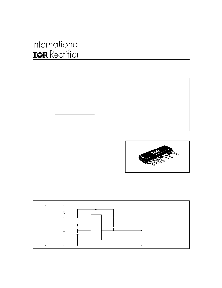
Typical Connection
Product Summary
f
=
+
1
1 4
R
75
C
T
T
. × (
) ×
1
D 1
2
3
4
6
7
9
V c c
C O M
V O
V
IN
V
B
IR51H(D)XXX
VIN
C O M
TO,
L O A D
D C B u s
R
T
C
T
R
T
C
T
External
Fast recovery diode D1 is
not required for HD type
IR51H(D)224
IR51H(D)320
IR51H(D)420
power MOSFETs are matched to simplify
use in 50% duty cycle applications. The
device can operate up to 500 volts.
2
IR51H(D)224
IR51H(D)320
IR51H(D)420
NOTE 1:
This IC contains a zener clamp structure between V
CC
and COM which has a nominal breakdown voltage of 15.6V.
Please note that this supply pin should not be driven by a DC, low impedance power source greater than the V
CLAMP
specified in the Electrical Characteristics Section
Symbol
Definition
Minimum
Maximum
Units
V
IN
High voltage supply
-224
- 0.3
250
-320
- 0.3
400
-420
- 0.3
500
V
B
High side floating supply
Vo - 0.3
Vo +2.5
V
O
Half-bridge output
-0.3
V
IN
+ 0.3
V
RT
R
T
voltage
- 0.3
V
cc
+ 0.3
V
CT
C
T
voltage
- 0.3
V
cc
+ 0.3
I
cc
Supply current (note 1)
--
25
I
RT
R
T
output current
- 5
5
dV/dt
Peak diode recovery
--
3.5
V/ns
P
D
Package power dissipation @ TA
+25°C
--
2.00
W
Rth
JA
Thermal resistance, junction to ambient
--
60
o
C/W
T
J
Junction temperature
-55
150
T
S
Storage temperature
-55
150
T
L
Lead temperature (soldering, 10 seconds)
--
300
Absolute Maximum Ratings
Absolute maximum ratings indicate sustained limits beyond which damage to the device may occur. All
voltage parameters are absolute voltages referenced to COM, all currents are defined positive into any
lead. The thermal resistance and power dissipation ratings are measured under board mounted and
still air conditions.
mA
o
C
V
3
IR51H(D)224
IR51H(D)320
IR51H(D)420
Recommended Operating Conditions
The input/output logic timing diagram is shown in figure 1. For proper operation, the device should be used
within the recommended conditions.
Symbol Definition
Minimum
Maximum
Units
V
B
High side floating supply absolute voltage
Vo + 10
Vo + Vclamp
V
IN
High voltage supply -224
--
250
-320
--
400
-420
--
500
V
O
Half-bridge output voltage
-3.0 (note 2)
V
IN
I
D
Continuous drain current (TA = 25°C)
-224
--
1.1
-320
--
0.9
-420
--
0.7
(TA = 85°C)
-224
--
0.7
-320
--
0.6
-420
--
0.5
I
CC
Supply current
(note 3)
5
mA
T
A
Ambient temperature
-40
125
°C
A
V
Dynamic Electrical Characteristics
V
BIAS
(V
CC
, V
BS
) = 12V, TA = 25
o
C unless otherwise specified.
Symbol Definition
Min. Typ. Max.
Units Test Conditions
trr
Reverse recovery time (MOSFET body diode)
-224
--
200
--
-320
--
270
--
-420
--
240
--
Qrr
Reverse recovery charge (MOSFET body diode) -224
--
0.7
--
-320
--
0.6
--
-420
--
0.5
--
D
R
T
duty cycle
--
50
--
% fosc = 20 kHz
I
F
=1.1A
I
F
=900mA
I
F
=700mA
I
F
=1.1A
I
F
=900mA
I
F
=700mA
ns
µ
C
di/dt
=100
A/
µ
s
NOTE 2:
Care should be taken to avoid switching conditions where the V
S
node flies inductively below ground by more than 5V.
NOTE 3:
Enough current should be supplied to the V
CC
lead of the IC to keep the internal 15.6V zener diode clamping the
voltage at this lead.
4
IR51H(D)224
IR51H(D)320
IR51H(D)420
Symbol Definition
Min. Typ. Max. UnitsTest Conditions
V
CCUV+
V
CC
supply undervoltage positive going
--
8.4
--
V
threshold
V
CCUV-
V
CC
supply undervoltage negative going
--
8.0
--
V
threshold
I
QCC
Quiescent V
CC
supply current
--
300
--
µ
A V
CC
> V
CCUV
V
CLAMP
V
CC
zener shunt clamp voltage
--
15.6
--
V I
CC
= 5mA
I
QBS
Quiescent V
BS
supply current
--
30
--
l
OS
Offset supply leakage current
--
--
50
V
B
= V
IN
= 500V
f
OSC
Oscillator frequency
--
20
--
R
T
= 35.7 k
C
T
= 1 nF
--
100
--
R
T
= 7.04 k
C
T
= 1 nF
I
CT
C
T
input current
--
0.001
1.0
µ
A
V
CTUV
C
T
undervoltage lockout
--
100
--
Note 2
V
RT+
R
T
high level output voltage, V
CC
- R
T
--
20
--
I
RT
= 100µA
--
200
--
I
RT
= -1mA
V
RT-
R
T
low level output voltage
--
20 -- I
RT
= 100µA
--
200
--
I
RT
= -1mA
V
RTUV
R
T
undervoltage lockout, V
CC
- R
T
--
100
--
I
RT
= 100µA
V
CT+
2/3 V
CC
threshold
--
8.0
--
V
CT-
1/3 V
CC
threshold
--
4.0
--
Static Electrical Characteristics
V
BIAS
(V
CC
, V
B
) = 12V, TA = 25
o
C unless otherwise specified.
Rds(on)
Static-drain-to-source on-resistance
-224
-- 1.1 --
-320
--
1.8
--
-420
--
3.0
--
V
SD
Diode forward voltage
-224
--
0.85
--
-320
--
0.7
--
-420
--
0.8
--
I
F
=1.1A
I
F
=900mA
I
F
=700mA
I
F
=1.1A
I
F
=900mA
I
F
=700mA
V
kHz
µ
A
kHz
mV
di/dt
=100
A/
µ
s
5
IR51H(D)224
IR51H(D)320
IR51H(D)420
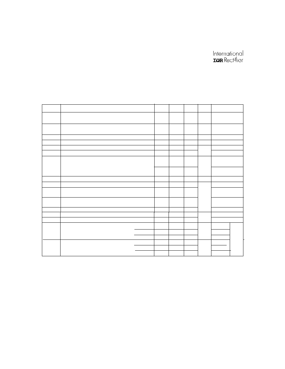
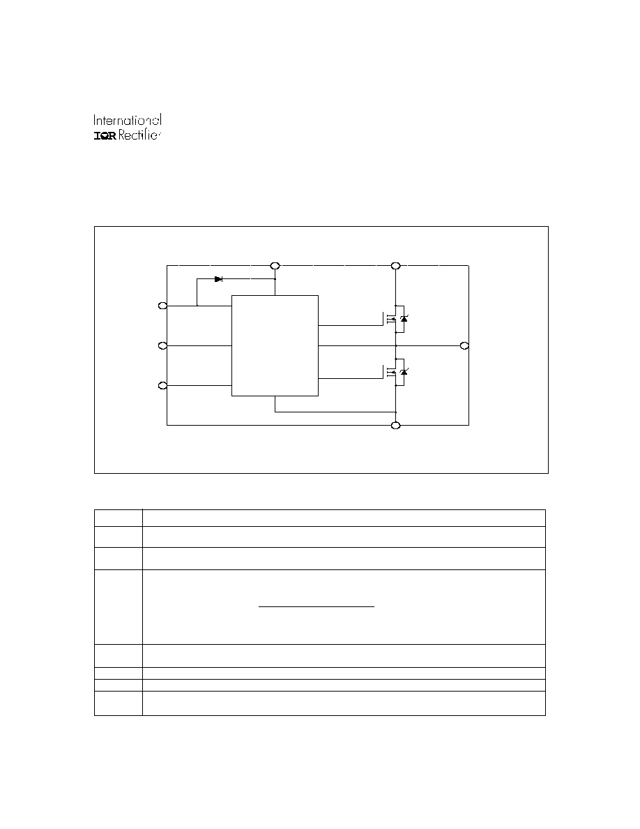
Functional Block Diagram
Symbol
Lead Description
V
CC
Logic and internal gate drive supply voltage. An internal zener clamp diode at 15.6 V norminal is included
to allow the V
CC
to be current fed directly from VIN typically by means of a high value resistor.
R
T
Oscillator timing resistor output; a resistor is connected from R
T
to C
T
. RT is out of phase with the half-
bridge output (VO).
C
T
Oscillator timing capacitor input; a capacitor is connected from C
T
to COM in order to program the
oscillator frequency according to the following equation:
C
T
PIN also invokes shutdown function (see note 2) where 75
is the effective impedence of the R
T
output stage.
V
B
High side gate drive floating supply. For bootstrap operation a high voltage fast recovery diode is needed
to feed from V
CC
to V
B
. (HD type circuits incorporate this diode).
V
IN
High voltage supply
VO
Half Bridge output
COM
Logic and low side of half bridge return
Lead Definitions
f
=
+
1
1 4
R
75
C
T
T
. × (
) ×
I R 2 1 5 1
D 1
V I N
V
B
C O M
V O
V c c
R
T
C
T
I R F C X X X
I R F C X X X
1
2
3
4
6
7
9
F a s t r e c o v e r y d i o d e D 1 i s
i n c o r p o r a t e d i n I R 5 1 H D X X X o n l y
H
O
V
S
L
O