Rev1.0
4/29/2005
IRDC3637EVAL
1
IR3637 EVALUATION BOARD USER GUIDE
DESCRIPTION
The IR3637 controller IC is designed to
provide a low cost synchronous Buck
regulator for on-board DC to DC
applications in a small 8-pin SOIC. The
output voltage can be precisely regulated
using the internal 0.8V reference voltage
for low voltage applications.
The IR3637 operates at a fixed internal
400KHz switching frequency to reduce the
component size.
The device features under-voltage lockout
for both input supplies, an external
programmable soft-start function as well as
output under-voltage detection that latches
off the device when an output short is
detected.
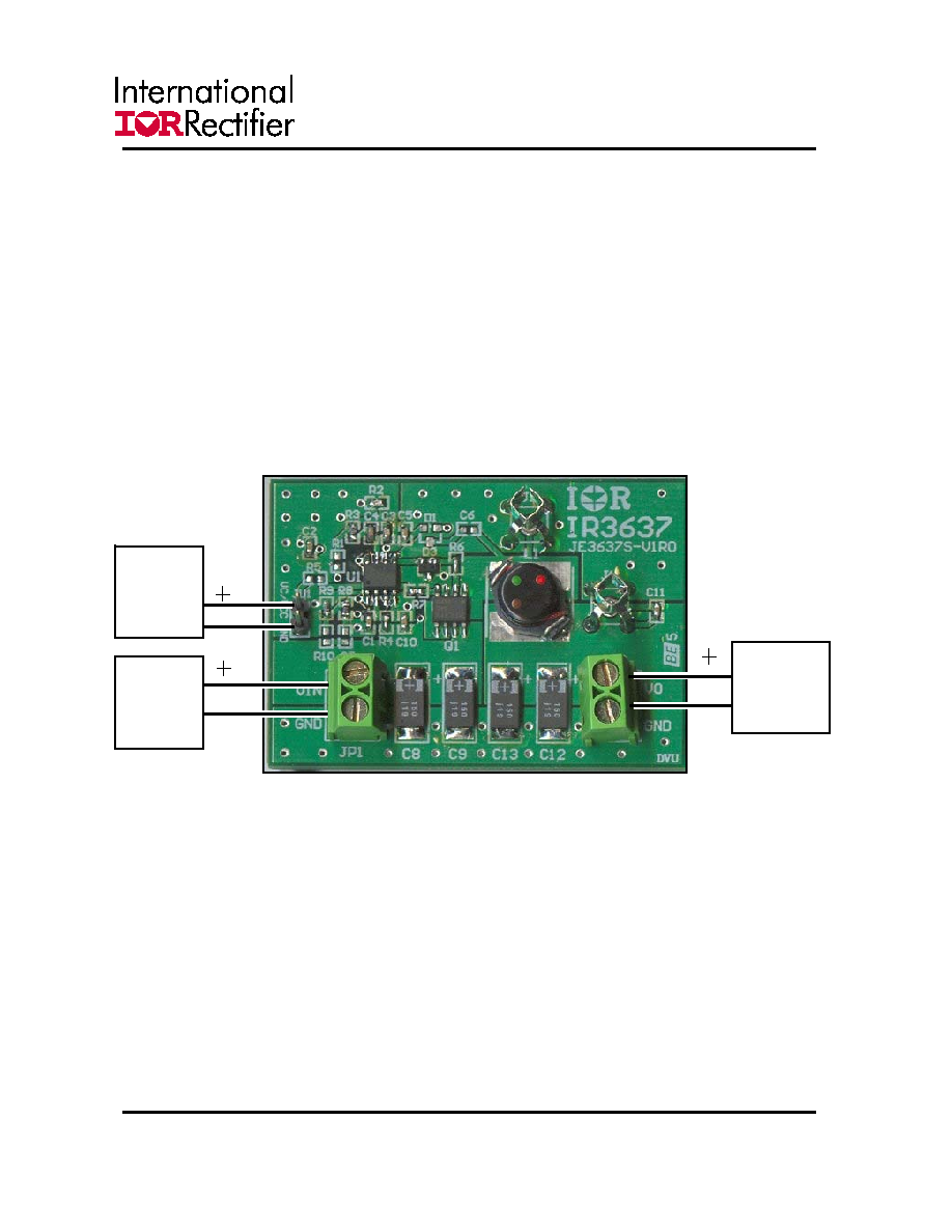
INPUT / OUTPUT CONNECTIONS
The following is the input / output connections:
Inputs:
JP1: Input (+5V) and GND
JU1: V
c
Outputs:
JP2: V
out
(+1.8V) and GND
Other Connections:
J1: Scope connection for V
out
J2: Scope connection for Inductor Point
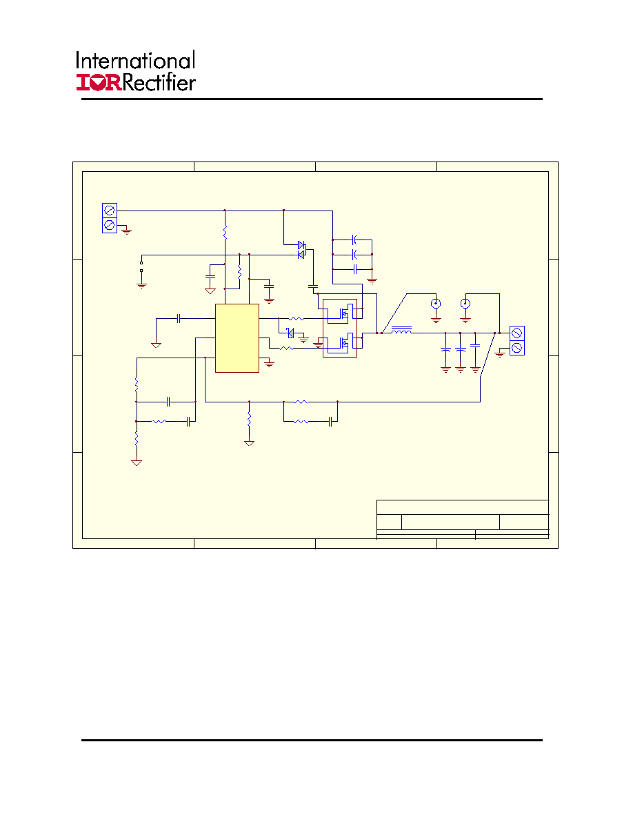
SPECIFICATION DATA
V
c
= 12V
V
cc
=V
in
=5V
V
out
=1.8V
Iout =7A
Output Ripple = 50mV
F
s
= 400KHz
The reference board is designed for
1.8V output using +5V and +12V
supplies. This will demonstrate the
main features of IC.
This user guide contains the schematic
and bill of materials, the design
guidelines are described in data sheet.
The connection points are shown in
Figure1. Connect the power supply
cables according to this figure,
minimizing wire lengths to reduce
losses in the wire. Test points J1 and
J2 provide easy connection for
oscilloscope voltage probe to monitor
the inductor points and output voltage.
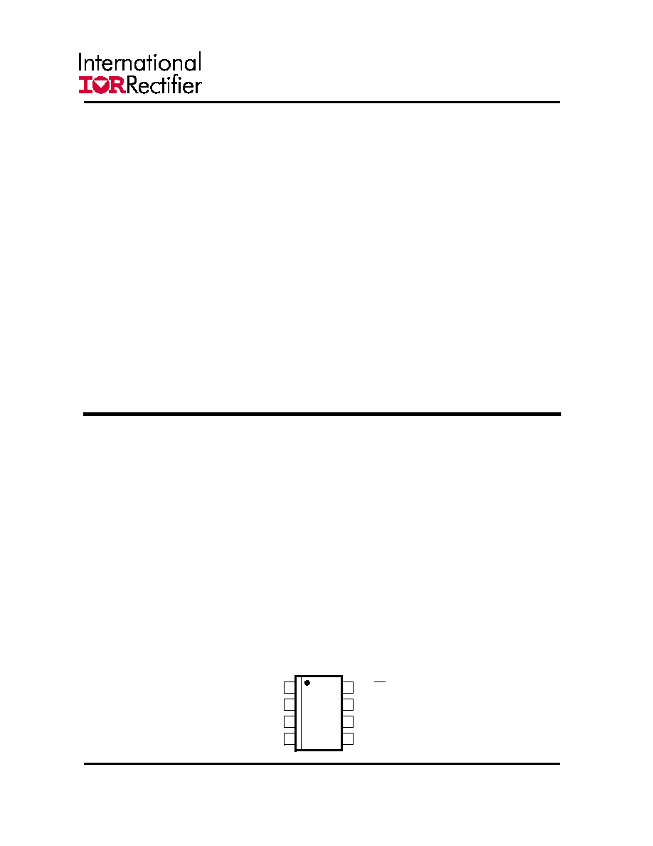
PACKAGE INFORMATION
Fb
Vcc
LDrv
Gnd
HDrv
Vc
Comp
SS/SD
4
3
2
1
5
6
7
8
Rev1.0
4/29/2005
IRDC3637EVAL
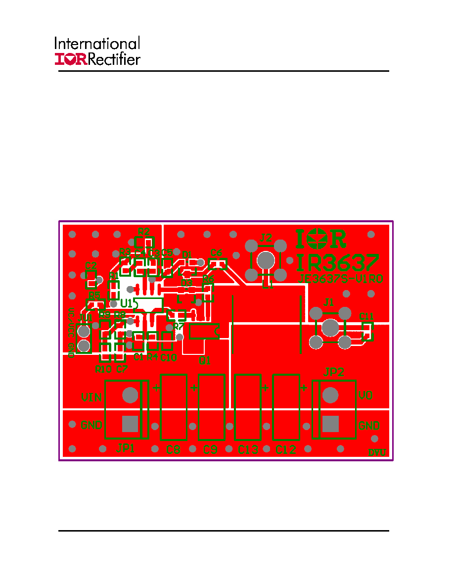
LAYOUT
The top side (component) layer for
IR3637 Eval board is shown in Figure
2. The input capacitors are all located
close to the MOSFETs. All the
decoupling capacitors, and feedback
components are located close to IC.
The feedback resistors are tied to the
output voltage at the point of
regulation.
The PCB is 4-layers board, one
layer is dedicated to Power GND
and the analog GND is kept
separated from the PGND and it is
connected at a single point.
Figure 2 Top layer of evaluation board for IR3637
3