 | –≠–ª–µ–∫—Ç—Ä–æ–Ω–Ω—ã–π –∫–æ–º–ø–æ–Ω–µ–Ω—Ç: IRF530S | –°–∫–∞—á–∞—Ç—å:  PDF PDF  ZIP ZIP |

Parameter
Typ.
Max.
Units
R
q
JC
Junction-to-Case
≠≠≠
2.0
R
q
JA
Junction-to-Ambient ( PCB Mounted,steady-state)**
≠≠≠
40
IRL5602S
HEXFET
Æ
Power MOSFET
Fifth Generation HEXFETs from International Rectifier utilize advanced
processing techniques to achieve extremely low on-resistance per silicon area.
This benefit, combined with the fast switching speed and ruggedized device
design that HEXFET Power MOSFETs are well known for, provides the
designer with an extremely efficient and reliable device for use in a wide variety
of applications.
The D
2
Pak is a surface mount power package capable of accommodating die
sizes up to HEX-4. It provides the highest power capability and the lowest
possible on-resistance in any existing surface mount package. The D
2
Pak is
suitable for high current applications because of its low internal connection
resistance and can dissipate up to 2.0W in a typical surface mount application.
Parameter
Max.
Units
I
D
@ T
C
= 25∞C
Continuous Drain Current, V
GS
@ -4.5V
-24
I
D
@ T
C
= 100∞C
Continuous Drain Current, V
GS
@ -4.5V
-17
A
I
DM
Pulsed Drain Current
-96
P
D
@T
C
= 25∞C
Power Dissipation
75
W
Linear Derating Factor
0.5
W/∞C
V
GS
Gate-to-Source Voltage
± 8.0
V
E
AS
Single Pulse Avalanche Energy
290
mJ
I
AR
Avalanche Current
-12
A
E
AR
Repetitive Avalanche Energy
7.5
mJ
dv/dt
Peak Diode Recovery dv/dt
-0.81
V/ns
T
J
Operating Junction and
-55 to + 175
T
STG
Storage Temperature Range
Soldering Temperature, for 10 seconds
300 (1.6mm from case )
∞C
Absolute Maximum Ratings
Thermal Resistance
V
DSS
= -20V
R
DS(on)
= 0.042
W
I
D
= -24A
l
Advanced Process Technology
l
Dynamic dv/dt Rating
l
175∞C Operating Temperature
l
P-Channel
l
Fast Switching
l
Fully Avalanche Rated
Description
5/11/99
www.irf.com
1
S
D
G
2
D Pak
∞C/W
PD- 91888
IRL5602S
2
www.irf.com
Parameter
Min. Typ. Max. Units
Conditions
I
S
Continuous Source Current
MOSFET symbol
(Body Diode)
≠≠≠
≠≠≠
showing the
I
SM
Pulsed Source Current
integral reverse
(Body Diode)
≠≠≠
≠≠≠
p-n junction diode.
V
SD
Diode Forward Voltage
≠≠≠
≠≠≠
-1.4
V
T
J
= 25∞C, I
S
= -12A, V
GS
= 0V
t
rr
Reverse Recovery Time
≠≠≠
58
88
ns
T
J
= 25∞C, I
F
= -12A
Q
rr
Reverse RecoveryCharge
≠≠≠
54
81
nC
di/dt = -100A/µs
t
on
Forward Turn-On Time
Intrinsic turn-on time is negligible (turn-on is dominated by L
S
+L
D
)
Repetitive rating; pulse width limited by
max. junction temperature. ( See fig. 11 )
I
SD
£
-12A, di/dt
£
120A/µs, V
DD
£
V
(BR)DSS
,
T
J
£
175∞C
Notes:
Starting T
J
= 25∞C, L = 3.0mH
R
G
= 25
W
, I
AS
= -14A. (See Figure 12)
Pulse width
£
300µs; duty cycle
£
2%.
Source-Drain Ratings and Characteristics
-24
-96
A
Parameter
Min. Typ. Max. Units
Conditions
V
(BR)DSS
Drain-to-Source Breakdown Voltage
-20
≠≠≠
≠≠≠
V
V
GS
= 0V, I
D
= -250µA
D
V
(BR)DSS
/
D
T
J
Breakdown Voltage Temp. Coefficient
≠≠≠
-0.013 ≠≠≠
V/∞C
Reference to 25∞C, I
D
= -1mA
≠≠≠
≠≠≠ 0.042
V
GS
= -4.5V, I
D
= -12A
≠≠≠
≠≠≠ 0.062
W
V
GS
= -2.7V, I
D
= -10A
≠≠≠
≠≠≠ 0.075
V
GS
= -2.5V, I
D
= -10A
V
GS(th)
Gate Threshold Voltage
-0.7
≠≠≠
-1.0
V
V
DS
= V
GS
, I
D
= -250µA
g
fs
Forward Transconductance
12
≠≠≠
≠≠≠
S
V
DS
= -15V, I
D
= -12A
≠≠≠
≠≠≠
-25
V
DS
= -20V, V
GS
= 0V
≠≠≠
≠≠≠
-250
V
DS
= -16V, V
GS
= 0V, T
J
= 150∞C
Gate-to-Source Forward Leakage
≠≠≠
≠≠≠
500
nA
V
GS
= -8.0V
Gate-to-Source Reverse Leakage
≠≠≠
≠≠≠
-500
V
GS
= 8.0V
Q
g
Total Gate Charge
≠≠≠
≠≠≠
44
I
D
= -12A
Q
gs
Gate-to-Source Charge
≠≠≠
≠≠≠
8.7
nC
V
DS
= -16V
Q
gd
Gate-to-Drain ("Miller") Charge
≠≠≠
≠≠≠
19
V
GS
= -4.5V, See Fig. 6 and 13
t
d(on)
Turn-On Delay Time
≠≠≠
9.7
≠≠≠
V
DD
= -10 V
t
r
Rise Time
≠≠≠
73
≠≠≠
I
D
= -12A
t
d(off)
Turn-Off Delay Time
≠≠≠
53
≠≠≠
R
G
= 6.0
W
, V
GS
= 4.5V
t
f
Fall Time
≠≠≠
84
≠≠≠
R
D
= 0.8
W
, See Fig. 10
Between lead,
≠≠≠
≠≠≠
and center of die contact
C
iss
Input Capacitance
≠≠≠
1460 ≠≠≠
V
GS
= 0V
C
oss
Output Capacitance
≠≠≠
790
≠≠≠
pF
V
DS
= -15V
C
rss
Reverse Transfer Capacitance
≠≠≠
370
≠≠≠
= 1.0MHz, See Fig. 5
Electrical Characteristics @ T
J
= 25∞C (unless otherwise specified)
nH
I
GSS
R
DS(on)
Static Drain-to-Source On-Resistance
L
S
Internal Source Inductance
7.5
ns
I
DSS
Drain-to-Source Leakage Current
µA
S
D
G
**
When mounted on FR-4 board using minimum recommended footprint.
For recommended footprint and soldering techniques refer to application note #AN-994.

IRL5602S
www.irf.com
3
Fig 4. Normalized On-Resistance
Vs. Temperature
Fig 2. Typical Output Characteristics
Fig 1. Typical Output Characteristics
Fig 3. Typical Transfer Characteristics
-60 -40 -20
0
20 40 60 80 100 120 140 160 180
0.0
0.5
1.0
1.5
2.0
2.5
3.0
3.5
T , Junction Temperature ( C)
R , Drain-to-Source On Resistance
(Normalized)
J
D
S
(
on)
∞
V
=
I =
GS
D
-4.5V
-24A
1
10
100
2.0
3.0
4.0
5.0
6.0
V = -15V
20µs PULSE WIDTH
DS
-V , Gate-to-Source Voltage (V)
-I , Drain-to-Source Current (A)
GS
D
T = 25 C
J
∞
T = 175 C
J
∞
1
10
100
0.1
1
10
100
20µs PULSE WIDTH
T = 25 C
J
∞
TOP
BOTTOM
VGS
-15V
-12V
-10V
-7.0V
-5.0V
-4.5V
-2.7V
-2.0V
-V , Drain-to-Source Voltage (V)
-I , Drain-to-Source Current (A)
DS
D
-2.0V
1
10
100
0.1
1
10
100
20µs PULSE WIDTH
T = 175 C
J
∞
TOP
BOTTOM
VGS
-15V
-12V
-10V
-7.0V
-5.0V
-4.5V
-2.7V
-2.0V
-V , Drain-to-Source Voltage (V)
-I , Drain-to-Source Current (A)
DS
D
-2.0V

IRL5602S
4
www.irf.com
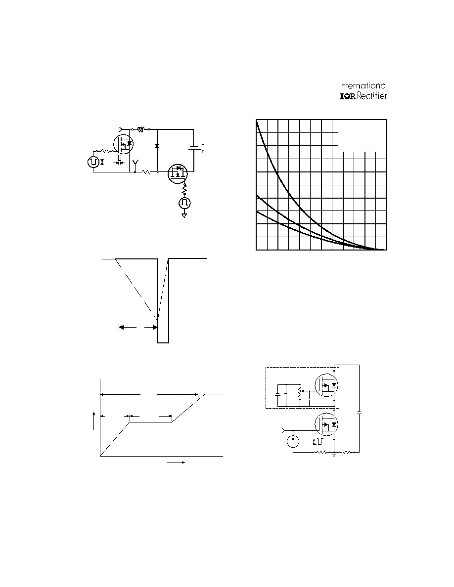
Fig 8. Maximum Safe Operating Area
Fig 6. Typical Gate Charge Vs.
Gate-to-Source Voltage
Fig 5. Typical Capacitance Vs.
Drain-to-Source Voltage
Fig 7. Typical Source-Drain Diode
Forward Voltage
1
10
100
0
400
800
1200
1600
2000
2400
2800
-V , Drain-to-Source Voltage (V)
C, Capacitance (pF)
DS
V
C
C
C
=
=
=
=
0V,
C
C
C
f = 1MHz
+ C
+ C
C SHORTED
GS
iss
gs
gd ,
ds
rss
gd
oss
ds
gd
C
iss
C
oss
C
rss
0
10
20
30
40
50
60
70
0
3
6
9
12
15
Q , Total Gate Charge (nC)
-V , Gate-to-Source Vol
t
age (V)
G
GS
FOR TEST CIRCUIT
SEE FIGURE
I =
D
13
-12A
V
=-10V
DS
V
=-16V
DS
0.1
1
10
100
0.0
0.4
0.8
1.2
1.6
-V ,Source-to-Drain Voltage (V)
-I , Reverse Drain Current (A)
SD
SD
V = 0 V
GS
T = 25 C
J
∞
T = 175 C
J
∞
1
10
100
1000
1
10
100
OPERATION IN THIS AREA LIMITED
BY R
DS(on)
Single Pulse
T
T
= 175 C
= 25 C
∞
∞
J
C
-V , Drain-to-Source Voltage (V)
-I , Drain Current (A)
I , Drain Current (A)
DS
D
100us
1ms
10ms

IRL5602S
www.irf.com
5
Fig 11. Maximum Effective Transient Thermal Impedance, Junction-to-Case
Fig 9. Maximum Drain Current Vs.
Case Temperature
0.01
0.1
1
10
0.00001
0.0001
0.001
0.01
0.1
Notes:
1. Duty factor D =
t / t
2. Peak T = P
x Z
+ T
1
2
J
DM
thJC
C
P
t
t
DM
1
2
t , Rectangular Pulse Duration (sec)
Ther
m
a
l
R
e
sponse
(Z
)
1
thJC
0.01
0.02
0.05
0.10
0.20
D = 0.50
SINGLE PULSE
(THERMAL RESPONSE)
25
50
75
100
125
150
175
0
5
10
15
20
25
T , Case Temperature
( C)
-I , Drain Current (A)
∞
C
D
V
DS
-4.5V
Pulse Width £ 1 µs
Duty Factor £ 0.1 %
R
D
V
GS
V
DD
R
G
D.U.T.
+
-
V
DS
90%
10%
V
GS
t
d(on)
t
r
t
d(off)
t
f
IRL5602S
6
www.irf.com
Fig 12c. Maximum Avalanche Energy
Vs. Drain Current
25
50
75
100
125
150
175
0
200
400
600
800
1000
Starting T , Junction Temperature ( C)
E ,
Si
ngl
e Pul
s
e Aval
anche Ener
gy (
m
J)
J
AS
∞
ID
TOP
BOTTOM
-5.9A
-10A
-14A
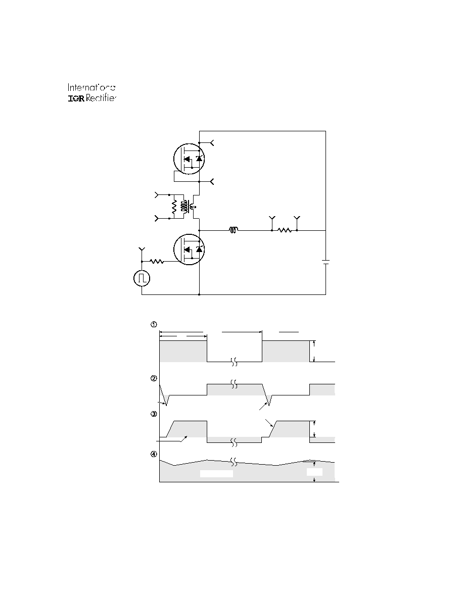
Fig 13b. Gate Charge Test Circuit
Fig 13a. Basic Gate Charge Waveform
Q
G
Q
GS
Q
GD
V
G
Charge
-4.5V
D.U.T.
V
DS
I
D
I
G
-3mA
V
GS
.3
µ
F
50K
.2
µ
F
12V
Current Regulator
Same Type as D.U.T.
Current Sampling Resistors
+
-
Fig 12b. Unclamped Inductive Waveforms
Fig 12a. Unclamped Inductive Test Circuit
tp
V
(BR)DSS
I
AS
R G
IAS
0.01
tp
D.U.T
L
VDS
VDD
DRIVER
A
15V
-20V
IRL5602S
www.irf.com
7
Peak Diode Recovery dv/dt Test Circuit
P.W.
Period
di/dt
Diode Recovery
dv/dt
Ripple
5%
Body Diode
Forward Drop
Re-Applied
Voltage
Reverse
Recovery
Current
Body Diode Forward
Current
V
GS
=10V
V
DD
I
SD
Driver Gate Drive
D.U.T. I
SD
Waveform
D.U.T. V
DS
Waveform
Inductor Curent
D =
P.W.
Period
+
-
+
+
+
-
-
-
R
G
V
DD
∑ dv/dt controlled by R
G
∑ I
SD
controlled by Duty Factor "D"
∑ D.U.T. - Device Under Test
D.U.T
*
Circuit Layout Considerations
∑ Low Stray Inductance
∑ Ground Plane
∑ Low Leakage Inductance
Current Transformer
*
Reverse Polarity of D.U.T for P-Channel
V
GS
[ ]
[ ]
***
V
GS
= 5.0V for Logic Level and 3V Drive Devices
[ ] ***
Fig 14. For P-Channel HEXFETS
IRL5602S
8
www.irf.com
WORLD HEADQUARTERS: 233 Kansas St., El Segundo, California 90245, Tel: (310) 322 3331
IR GREAT BRITAIN: Hurst Green, Oxted, Surrey RH8 9BB, UK Tel: ++ 44 1883 732020
IR CANADA: 15 Lincoln Court, Brampton, Ontario L6T3Z2, Tel: (905) 453 2200
IR GERMANY: Saalburgstrasse 157, 61350 Bad Homburg Tel: ++ 49 6172 96590
IR ITALY: Via Liguria 49, 10071 Borgaro, Torino Tel: ++ 39 11 451 0111
IR FAR EAST: K&H Bldg., 2F, 30-4 Nishi-Ikebukuro 3-Chome, Toshima-Ku, Tokyo Japan 171 Tel: 81 3 3983 0086
IR SOUTHEAST ASIA: 1 Kim Seng Promenade, Great World City West Tower, 13-11, Singapore 237994 Tel: ++ 65 838 4630
IR TAIWAN:16 Fl. Suite D. 207, Sec. 2, Tun Haw South Road, Taipei, 10673, Taiwan Tel: 886-2-2377-9936
http://www.irf.com/ Data and specifications subject to change without notice. 5/99
3
4
4
TRR
FEED DIRECTION
1.85 (.073)
1.65 (.065)
1.60 (.063)
1.50 (.059)
4.10 (.161)
3.90 (.153)
TRL
FEED DIRECTION
10.90 (.429)
10.70 (.421)
16.10 (.634)
15.90 (.626)
1.75 (.069)
1.25 (.049)
11.60 (.457)
11.40 (.449)
15.42 (.609)
15.22 (.601)
4.72 (.136)
4.52 (.178)
24.30 (.957)
23.90 (.941)
0.368 (.0145)
0.342 (.0135)
1.60 (.063)
1.50 (.059)
13.50 (.532)
12.80 (.504)
330.00
(14.173)
MAX.
27.40 (1.079)
23.90 (.941)
60.00 (2.362)
MIN.
30.40 (1.197)
MAX.
26.40 (1.039)
24.40 (.961)
NOTES :
1. COMFORMS TO EIA-418.
2. CONTROLLING DIMENSION: MILLIMETER.
3. DIMENSION MEASURED @ HUB.
4. INCLUDES FLANGE DISTORTION @ OUTER EDGE.
10.16 (.400)
REF.
6.47 (.255)
6.18 (.243)
2.61 (.103)
2.32 (.091)
8.89 (.350)
REF.
- B -
1.32 (.052)
1.22 (.048)
2.79 (.110)
2.29 (.090)
1.39 (.055)
1.14 (.045)
5.28 (.208)
4.78 (.188)
4.69 (.185)
4.20 (.165)
10.54 (.415)
10.29 (.405)
- A -
2
1 3
15.49 (.610)
14.73 (.580)
3X
0.93 (.037)
0.69 (.027)
5.08 (.200)
3X
1.40 (.055)
1.14 (.045)
1.78 (.070)
1.27 (.050)
1.40 (.055)
MAX.
NOTES:
1 DIMENSIONS AFTER SOLDER DIP.
2 DIMENSIONING & TOLERANCING PER ANSI Y14.5M, 1982.
3 CONTROLLING DIMENSION : INCH.
4 HEATSINK & LEAD DIMENSIONS DO NOT INCLUDE BURRS.
0.55 (.022)
0.46 (.018)
0.25 (.010) M B A M
MINIMUM RECOMMENDED FOOTPRINT
11.43 (.450)
8.89 (.350)
17.78 (.700)
3.81 (.150)
2.08 (.082)
2X
LEAD ASSIGNMENTS
1 - GATE
2 - DRAIN
3 - SOURCE
2.54 (.100)
2X
Tape & Reel
TO-263AB Package Details
Part Marking
(This is an IRF530S with assembly lot
code 9B1M )
PART NUMBER
INTERNATIONAL
RECTIFIER
LOGO
DATE CODE
(YYWW)
YY = YEAR
WW = WEEK
ASSEMBLY
LOT CODE
F530S
9B 1M
9246
A