 | ÐлекÑÑоннÑй компоненÑ: IRF6662 | СкаÑаÑÑ:  PDF PDF  ZIP ZIP |
Äîêóìåíòàöèÿ è îïèñàíèÿ www.docs.chipfind.ru
www.irf.com
1
08/05/05
IRF6662
DirectFETTM Power MOSFET
DirectFETTM ISOMETRIC
MZ
PD - 97039
Applicable DirectFET Outline and Substrate Outline (see p.7,8 for details)
Fig 1. Typical On-Resistance vs. Gate Voltage
Typical values (unless otherwise specified)
Description
The IRF6662 combines the latest HEXFET® Power MOSFET Silicon technology with the advanced DirectFET
TM
packaging to achieve the
lowest on-state resistance in a package that has the footprint of an SO-8 and only 0.7 mm profile. The DirectFET package is compatible with
existing layout geometries used in power applications, PCB assembly equipment and vapor phase, infra-red or convection soldering techniques,
when application note AN-1035 is followed regarding the manufacturing methods and processes. The DirectFET package allows dual sided
cooling to maximize thermal transfer in power systems, improving previous best thermal resistance by 80%.
The IRF6662 is optimized for primary side bridge topologies in isolated DC-DC applications, for wide range universal input Telecom applications
(36V - 75V), and for secondary side synchronous rectification in regulated DC-DC topologies. The reduced total losses in the device coupled
with the high level of thermal performance enables high efficiency and low temperatures, which are key for system reliability improvements,
and makes this device ideal for high performance isolated DC-DC converters.
Lead and Bromide Free
Low Profile (<0.7 mm)
Dual Sided Cooling Compatible
Ultra Low Package Inductance
Optimized for High Frequency Switching
Ideal for High Performance Isolated Converter
Primary Switch Socket
Optimized for Synchronous Rectification
Low Conduction Losses
Compatible with existing Surface Mount Techniques
Click on this section to link to the appropriate technical paper.
Click on this section to link to the DirectFET Website.
Surface mounted on 1 in. square Cu board, steady state.
T
C
measured with thermocouple mounted to top (Drain) of part.
Repetitive rating; pulse width limited by max. junction temperature.
Starting T
J
= 25°C, L = 3.2mH, R
G
= 25
, I
AS
= 4.9A.
Notes:
SQ
SX
ST
MQ
MX
MT
MZ
Absolute Maximum Ratings
Parameter
Units
V
DS
Drain-to-Source Voltage
V
V
GS
Gate-to-Source Voltage
I
D
@ T
A
= 25°C
Continuous Drain Current, V
GS
@ 10V
I
D
@ T
A
= 70°C
Continuous Drain Current, V
GS
@ 10V
A
I
D
@ T
C
= 25°C
Continuous Drain Current, V
GS
@ 10V
I
DM
Pulsed Drain Current
E
AS
Single Pulse Avalanche Energy
mJ
I
AR
Avalanche Current
A
39
Max.
6.6
47
66
±20
100
8.3
4.9
V
DSS
V
GS
R
DS(on)
100V max ±20V max 17.5m
@ 10V
Q
g tot
Q
gd
V
gs(th)
22nC
6.8nC
3.9V
0
5
10
15
20
25
QG Total Gate Charge (nC)
0.0
2.0
4.0
6.0
8.0
10.0
12.0
V
G
S
,
G
a
t
e
-
t
o
-
S
o
u
r
c
e
V
o
l
t
a
g
e
(
V
)
VDS= 80V
VDS= 50V
VDS= 20V
ID= 4.9A
Fig 2. Typical Total Gate Charge vs.
Gate-to-Source Voltage
4
6
8
10
12
14
16
VGS, Gate -to -Source Voltage (V)
0
20
40
60
80
100
T
y
p
i
c
a
l
R
D
S
(
o
n
)
(
m
)
ID = 4.9A
TJ = 25°C
TJ = 125°C
IRF6662
2
www.irf.com
Notes:
Pulse width
400µs; duty cycle 2%.
Repetitive rating; pulse width limited by max. junction temperature.
S
D
G
Static @ T
J
= 25°C (unless otherwise specified)
Parameter
Min.
Typ.
Max. Units
BV
DSS
Drain-to-Source Breakdown Voltage
100
V
V
DSS
/
T
J
Breakdown Voltage Temp. Coefficient
0.10
V/°C
R
DS(on)
Static Drain-to-Source On-Resistance
17.5
22
m
V
GS(th)
Gate Threshold Voltage
3.0
4.9
V
V
GS(th)
/
T
J
Gate Threshold Voltage Coefficient
-9.7
mV/°C
I
DSS
Drain-to-Source Leakage Current
20
µA
250
I
GSS
Gate-to-Source Forward Leakage
100
nA
Gate-to-Source Reverse Leakage
-100
gfs
Forward Transconductance
11
S
Q
g
Total Gate Charge
22
31
Q
gs1
Pre-Vth Gate-to-Source Charge
4.9
Q
gs2
Post-Vth Gate-to-Source Charge
1.2
nC
Q
gd
Gate-to-Drain Charge
6.8
10
Q
godr
Gate Charge Overdrive
9.1
See Fig. 17
Q
sw
Switch Charge (Q
gs2
+ Q
gd
)
8.0
Q
oss
Output Charge
11
nC
R
G
Gate Resistance
1.2
t
d(on)
Turn-On Delay Time
11
t
r
Rise Time
7.5
t
d(off)
Turn-Off Delay Time
24
ns
t
f
Fall Time
5.9
C
iss
Input Capacitance
1360
C
oss
Output Capacitance
270
pF
C
rss
Reverse Transfer Capacitance
61
C
oss
Output Capacitance
1340
C
oss
Output Capacitance
160
Diode Characteristics
Parameter
Min.
Typ.
Max. Units
I
S
Continuous Source Current
2.5
(Body Diode)
A
I
SM
Pulsed Source Current
66
(Body Diode)
V
SD
Diode Forward Voltage
1.3
V
t
rr
Reverse Recovery Time
34
51
ns
Q
rr
Reverse Recovery Charge
50
75
nC
MOSFET symbol
R
G
=6.2
V
DS
= 25V
Conditions
V
GS
= 0V, V
DS
= 80V, f=1.0MHz
V
GS
= 0V, V
DS
= 1.0V, f=1.0MHz
V
DS
= 16V, V
GS
= 0V
V
DD
= 50V, V
GS
= 10V
V
GS
= 0V
= 1.0MHz
I
D
= 4.9A
V
DS
= V
GS
, I
D
= 100µA
V
DS
= 100V, V
GS
= 0V
Conditions
V
GS
= 0V, I
D
= 250µA
Reference to 25°C, I
D
= 1mA
V
GS
= 10V, I
D
= 8.2A
T
J
= 25°C, I
F
= 4.9A, V
DD
= 50V
di/dt = 100A/µs
T
J
= 25°C, I
S
= 4.9A, V
GS
= 0V
showing the
integral reverse
p-n junction diode.
I
D
= 4.9A
V
DS
= 80V, V
GS
= 0V, T
J
= 125°C
V
GS
= 20V
V
GS
= -20V
V
GS
= 10V
V
DS
= 10V, I
D
= 4.9A
V
DS
= 50V
IRF6662
www.irf.com
3
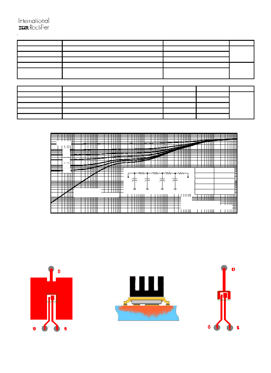
Fig 3. Maximum Effective Transient Thermal Impedance, Junction-to-Ambient
Surface mounted on 1 in. square Cu
board (still air).
Mounted on minimum
footprint full size board with
metalized back and with small
clip heatsink (still air)
Mounted to a PCB with
small clip heatsink (still air)
Surface mounted on 1 in. square Cu board, steady state.
Used double sided cooling , mounting pad.
Mounted on minimum footprint full size board with metalized
back and with small clip heatsink.
Notes:
T
C
measured with thermocouple incontact with top (Drain) of part.
R
is measured at
T
J
of approximately 90°C.
1E-006
1E-005
0.0001
0.001
0.01
0.1
1
10
100
t1 , Rectangular Pulse Duration (sec)
0.001
0.01
0.1
1
10
100
T
h
e
r
m
a
l
R
e
s
p
o
n
s
e
(
Z
t
h
J
A
)
0.20
0.10
D = 0.50
0.02
0.01
0.05
SINGLE PULSE
( THERMAL RESPONSE )
Notes:
1. Duty Factor D = t1/t2
2. Peak Tj = P dm x Zthja + Tc
Ri (°C/W)
i (sec)
1.2801 0.000322
8.7256 0.164798
21.7500 2.2576
13.2511 69
Absolute Maximum Ratings
Parameter
Units
P
D
@T
A
= 25°C
Power Dissipation
W
P
D
@T
A
= 70°C
Power Dissipation
P
D
@T
C
= 25°C
Power Dissipation
T
P
Peak Soldering Temperature
°C
T
J
Operating Junction and
T
STG
Storage Temperature Range
Thermal Resistance
Parameter
Typ.
Max.
Units
R
JA
Junction-to-Ambient
45
R
JA
Junction-to-Ambient
12.5
R
JA
Junction-to-Ambient
20
°C/W
R
JC
Junction-to-Case
1.4
R
J-PCB
Junction-to-PCB Mounted
1.0
270
-40 to + 150
Max.
89
2.8
1.8
J
J
1
1
2
2
3
3
R
1
R
1
R
2
R
2
R
3
R
3
Ci
i/Ri
Ci=
i/Ri
A
A
4
4
R
4
R
4
IRF6662
4
www.irf.com
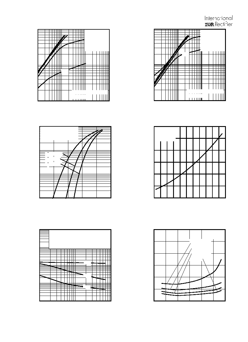
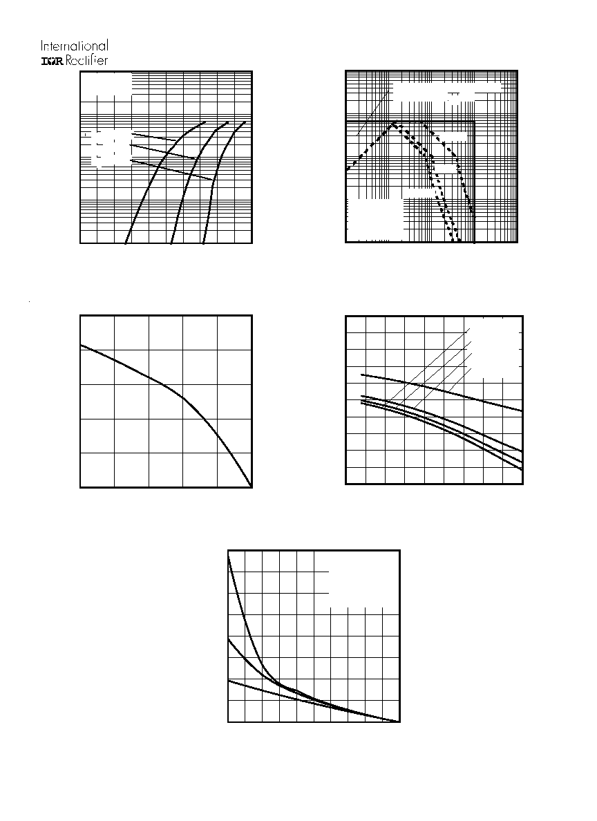
Fig 5. Typical Output Characteristics
Fig 4. Typical Output Characteristics
Fig 6. Typical Transfer Characteristics
Fig 7. Normalized On-Resistance vs. Temperature
Fig 8. Typical Capacitance vs.Drain-to-Source Voltage
0.1
1
10
100
VDS, Drain-to-Source Voltage (V)
1
10
100
I D
,
D
r
a
i
n
-
t
o
-
S
o
u
r
c
e
C
u
r
r
e
n
t
(
A
)
VGS
TOP 15V
10V
8.0V
7.0V
BOTTOM
6.0V
60µs PULSE WIDTH
Tj = 25°C
6.0V
3
4
5
6
7
8
VGS, Gate-to-Source Voltage (V)
0.1
1
10
100
I D
,
D
r
a
i
n
-
t
o
-
S
o
u
r
c
e
C
u
r
r
e
n
t
(
)
TJ = 150°C
TJ = 25°C
TJ = -40°C
VDS = 10V
60µs PULSE WIDTH
1
10
100
VDS, Drain-to-Source Voltage (V)
10
100
1000
10000
100000
C
,
C
a
p
a
c
i
t
a
n
c
e
(
p
F
)
VGS = 0V, f = 1 MHZ
Ciss = Cgs + Cgd, C ds SHORTED
Crss = Cgd
Coss = Cds + Cgd
Coss
Crss
Ciss
-60 -40 -20 0 20 40 60 80 100 120 140 160
TJ , Junction Temperature (°C)
0.5
1.0
1.5
2.0
T
y
p
i
c
a
l
R
D
S
(
o
n
)
(
N
o
r
m
a
l
i
z
e
d
)
VGS = 10V
ID = 8.2A
0.1
1
10
100
VDS, Drain-to-Source Voltage (V)
1
10
100
I D
,
D
r
a
i
n
-
t
o
-
S
o
u
r
c
e
C
u
r
r
e
n
t
(
A
)
6.0V
60µs PULSE WIDTH
Tj = 150°C
VGS
TOP 15V
10V
8.0V
7.0V
BOTTOM
6.0V
Fig 9. Typical On-Resistance vs. Drain Current
0
10
20
30
40
50
60
ID, Drain Current (A)
15
20
25
30
35
40
45
T
y
p
i
c
a
l
R
D
S
(
o
n
)
(
m
)
TJ = 25°C
Vgs = 7.0V
Vgs = 8.0V
Vgs = 10V
Vgs = 15V
IRF6662
www.irf.com
5
Fig 13. Typical Threshold Voltage vs.
Junction Temperature
Fig 12. Maximum Drain Current vs. Ambient Temperature
Fig 10. Typical Source-Drain Diode Forward Voltage
Fig11. Maximum Safe Operating Area
Fig 14. Maximum Avalanche Energy vs. Drain Current
25
50
75
100
125
150
Starting TJ , Junction Temperature (°C)
0
20
40
60
80
100
120
140
160
E
A
S
,
S
i
n
g
l
e
P
u
l
s
e
A
v
a
l
a
n
c
h
e
E
n
e
r
g
y
(
m
J
)
ID
TOP
1.6A
1.9A
BOTTOM 4.9A
0
1
10
100
1000
VDS, Drain-to-Source Voltage (V)
0.1
1
10
100
1000
I D
,
D
r
a
i
n
-
t
o
-
S
o
u
r
c
e
C
u
r
r
e
n
t
(
A
)
OPERATION IN THIS AREA
LIMITED BY RDS(on)
TA = 25°C
Tj = 150°C
Single Pulse
100µsec
1msec
10msec
25
50
75
100
125
150
TA , Ambient Temperature (°C)
0
2
4
6
8
10
I D
,
D
r
a
i
n
C
u
r
r
e
n
t
(
A
)
0.1 0.2 0.3 0.4 0.5 0.6 0.7 0.8 0.9 1.0 1.1
VSD, Source-to-Drain Voltage (V)
0
1
10
100
1000
I S
D
,
R
e
v
e
r
s
e
D
r
a
i
n
C
u
r
r
e
n
t
(
A
)
TJ = 150°C
TJ = 25°C
TJ = -40°C
VGS = 0V
-75 -50 -25
0
25
50
75 100 125 150
TJ , Temperature ( °C )
2.0
3.0
4.0
5.0
6.0
7.0
T
y
p
i
c
a
l
V
G
S
(
t
h
)
G
a
t
e
t
h
r
e
s
h
o
l
d
V
o
l
t
a
g
e
(
V
)
ID = 100µA
ID = 250µA
ID = 1.0mA
ID = 1.0A