Äîêóìåíòàöèÿ è îïèñàíèÿ www.docs.chipfind.ru
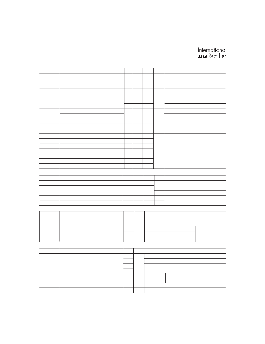
Parameter
Maximum
Units
I
D
@ T
A
= 25°C
Continuous Drain Current, V
GS
@ -10V
-4.7
A
I
D
@ T
A
= 70°C
-3.8
I
DM
Pulsed Drain Current
À
-38
P
D
@T
A
= 25°C
Power Dissipation
2.0
W
P
D
@T
A
= 70°C
1.3
Linear Derating Factor
16
mW/°C
V
GS
Gate-to-Source Voltage
± 20
V
dv/dt
Peak Diode Recovery dv/dt
Á
-5.0
V/ns
T
J,
T
STG
Junction and Storage Temperature Range
-55 to +150
°C
l
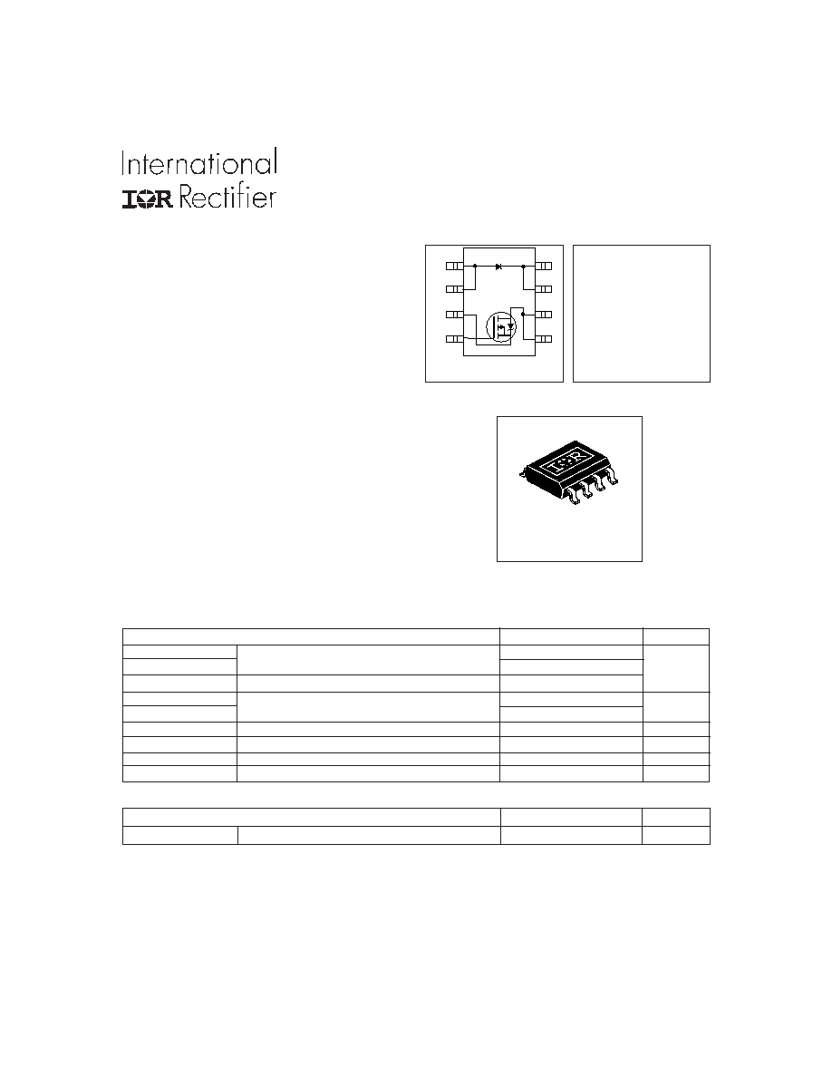
Co-packaged HEXFET
® Power
MOSFET and Schottky Diode
l
Ideal For Buck Regulator Applications
l
P-Channel HEXFET
®
l
Low V
F
Schottky Rectifier
l
Generation 5 Technology
l
SO-8 Footprint
l
Lead-Free
IRF7321D2PbF
10/12/04
FETKY
MOSFET & Schottky Diode
Absolute Maximum Ratings
( T
A
= 25°C Unless Otherwise Noted)
TM
Description
SO-8
V
DSS
= -30V
R
DS(on)
= 0.062
Schottky Vf = 0.52V
The FETKY
TM
family of Co-packaged HEXFETs and
Schottky diodes offer the designer an innovative board
space saving solution for switching regulator and
power management applications. Generation 5
HEXFETs utilize advanced processing techniques to
achieve extremely low on-resistance per silicon area.
Combinining this technology with International
Rectifier's low forward drop Schottky rectifiers results in
an extremely efficient device suitable for use in a wide
variety of portable electronics applications.
The SO-8 has been modified through a customized
leadframe for enhanced thermal characteristics. The
SO-8 package is designed for vapor phase, infrared or
wave soldering techniques.
Top View
8
1
2
3
4
5
6
7
A
A
S
G
D
D
K
K
Parameter
Maximum
Units
R
JA
Junction-to-Ambient
Ã
62.5
°C/W
Thermal Resistance Ratings
Notes:
Repetitive rating pulse width limited by max. junction temperature (see fig. 11)
I
SD
-2.9A, di/dt -77A/µs, V
DD
V
(BR)DSS
, T
J
150°C
Pulse width
300µs duty cycle 2%
Surface mounted on FR-4 board, t 10sec.
www.irf.com
PD - 95297
IRF7321D2PbF
2
www.irf.com
Parameter
Min. Typ. Max. Units
Conditions
V
(BR)DSS
Drain-to-Source Breakdown Voltage
-30
V
V
GS
= 0V, I
D
= -250µA
0.042 0.062
V
GS
= -10V, I
D
= -4.9A
0.076 0.098
V
GS
= -4.5V, I
D
= -3.6A
V
GS(th)
Gate Threshold Voltage
-1.0
V
V
DS
= V
GS
, I
D
= -250µA
g
fs
Forward Transconductance
7.7
S
V
DS
= -15V, I
D
= -4.9A
-1.0
V
DS
= -24V, V
GS
= 0V
-25
V
DS
= -24V, V
GS
= 0V, T
J
= 55°C
Gate-to-Source Forward Leakage
100
V
GS
= -20V
Gate-to-Source Reverse Leakage
-100
V
GS
= 20V
Q
g
Total Gate Charge
23
34
I
D
= -4.9A
Q
gs
Gate-to-Source Charge
3.8
5.7
nC
V
DS
= -15V
Q
gd
Gate-to-Drain ("Miller") Charge
5.9
8.9
V
GS
= -10V, See Fig. 6
t
d(on)
Turn-On Delay Time
13
19
V
DD
= -15V
t
r
Rise Time
13
20
I
D
= -1.0A
t
d(off)
Turn-Off Delay Time
34
51
R
G
= 6.0
t
f
Fall Time
32
48
R
D
= 15
,
C
iss
Input Capacitance
710
V
GS
= 0V
C
oss
Output Capacitance
380
pF
V
DS
= -25V
C
rss
Reverse Transfer Capacitance
180
= 1.0MHz, See Fig. 5
MOSFET Electrical Characteristics @ T
J
= 25°C (unless otherwise specified)
R
DS(on)
Static Drain-to-Source On-Resistance
I
DSS
Drain-to-Source Leakage Current
I
GSS
µA
nA
ns
Parameter
Min. Typ. Max. Units
Conditions
I
S
Continuous Source Current(Body Diode)
-2.5
I
SM
Pulsed Source Current (Body Diode)
-30
V
SD
Body Diode Forward Voltage
-0.78 -1.0
V
T
J
= 25°C, I
S
= -1.7A, V
GS
= 0V
t
rr
Reverse Recovery Time (Body Diode)
44
66
ns
T
J
= 25°C, I
F
= -1.7A
Q
rr
Reverse Recovery Charge
42
63
nC
di/dt = 100A/µs
A
MOSFET Source-Drain Ratings and Characteristics
Parameter
Max. Units
Conditions
If (av)
Max. Average Forward Current
3.2
50% Duty Cycle. Rectangular Wave, Tc = 25°C
2.0
See Fig.14
Tc = 70°C
I
SM
Max. peak one cycle Non-repetitive
200
5µs sine or 3µs Rect. pulse
Following any rated
Surge current
20
10ms sine or 6ms Rect. pulse load condition &
with Vrrm applied
A
Schottky Diode Maximum Ratings
A
Parameter
Max. Units
Conditions
Vfm
Max. Forward voltage drop
0.57
If = 3.0, Tj = 25°C
0.77
If = 6.0, Tj = 25°C
0.52
If = 3.0, Tj = 125°C
0.79
If = 6.0, Tj = 125°C
.
Irm
Max. Reverse Leakage current
0.30
Vr = 30V
Tj = 25°C
37
Tj = 125°C
Ct
Max. Junction Capacitance
310
pF
Vr = 5Vdc ( 100kHz to 1 MHz) 25°C
dv/dt
Max. Voltage Rate of Charge
4900 V/µs Rated Vr
Schottky Diode Electrical Specifications
V
mA
( HEXFET is the reg. TM for International Rectifier Power MOSFET's )
IRF7321D2PbF
www.irf.com
3
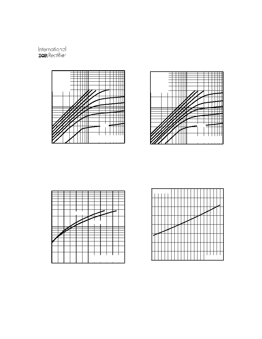
Fig 3. Typical Transfer Characteristics
Fig 2. Typical Output Characteristics
Fig 1. Typical Output Characteristics
1
10
100
0.1
1
10
D
DS
20µs PULSE WIDTH
T = 25°C
A
-I
,
D
r
ai
n-t
o
-S
ource C
u
rrent
(A
)
-V , Drain-to-Source Voltage (V)
J
-3.0V
VGS
TOP - 15V
- 10V
- 7.0V
- 5.5V
- 4.5V
- 4.0V
- 3.5V
BOTTOM - 3.0V
1
10
100
0.1
1
10
D
DS
A
-I
,
D
r
ai
n-t
o
-S
ource C
u
rrent
(A
)
-V , Drain-to-Source Voltage (V)
-3.0V
VGS
TOP - 15V
- 10V
- 7.0V
- 5.5V
- 4.5V
- 4.0V
- 3.5V
BOTTOM - 3.0V
20µs PULSE WIDTH
T = 150°C
J
1
10
100
3.0
3.5
4.0
4.5
5.0
5.5
6.0
T = 25°C
T = 150°C
J
J
GS
D
A
-
I
,
D
r
ai
n-
t
o
-
S
our
ce C
u
r
r
ent
(
A
)
-V , Gate-to-Source Voltage (V)
V = -10V
20µs PULSE WIDTH
DS
Fig 4. Normalized On-Resistance
Vs. Temperature
-60 -40 -20 0
20 40 60 80 100 120 140 160
0.0
0.5
1.0
1.5
2.0
T , Junction Temperature ( C)
R , Drain-to-Source On Resistance
(Normalized)
J
D
S
(
on)
°
V
=
I =
GS
D
10V
4.9A
-
-
-
4.9A
-
10V
Power Mosfet Characteristics
IRF7321D2PbF
4
www.irf.com
1
10
100
1
10
100
OPERATION IN THIS AREA LIMITED
BY R
DS(on)
Single Pulse
T
T
= 150 C
= 25 C
°
°
J
C
-V , Drain-to-Source Voltage (V)
-
I
,
D
r
ai
n C
u
r
r
ent
(
A
)
I
,
D
r
ai
n C
u
r
r
ent
(
A
)
DS
D
100us
1ms
10ms
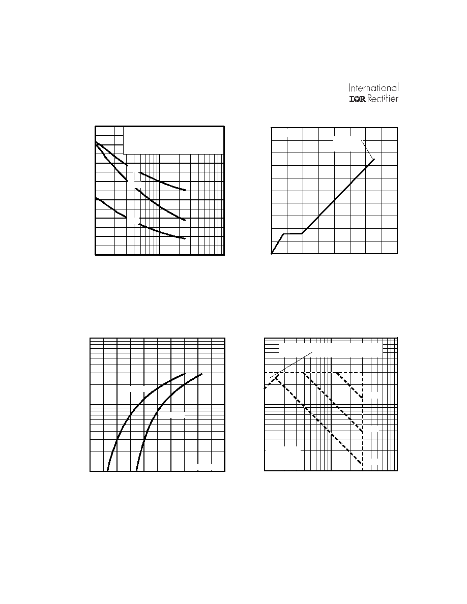
Fig 8. Maximum Safe Operating Area
Fig 6. Typical Gate Charge Vs.
Gate-to-Source Voltage
Fig 5. Typical Capacitance Vs.
Drain-to-Source Voltage
0
200
400
600
800
1000
1200
1400
1
10
100
C
,
C
apaci
t
ance (pF
)
DS
V , Drain-to-Source Voltage (V)
A
C
iss
C
oss
C
rss
V
GS
= 0V f = 1 MHz
Ciss = Cgs + Cgd + Cds SHORTED
Crss = Cgd
Coss = Cds + Cgd
-
0
10
20
30
40
0
4
8
12
16
20
Q , Total Gate Charge (nC)
-V , Gate-to-Source Voltage (V)
G
GS
I =
D
-4.9A
V
=-15V
DS
Fig 7. Typical Source-Drain Diode
Forward Voltage
1
10
100
0.4
0.6
0.8
1.0
1.2
1.4
T = 25°C
T = 150°C
J
J
V = 0V
GS
SD
SD
A
-I , Reverse Drain Current (A)
-V , Source-to-Drain Voltage (V)
Power Mosfet Characteristics
IRF7321D2PbF
www.irf.com
5
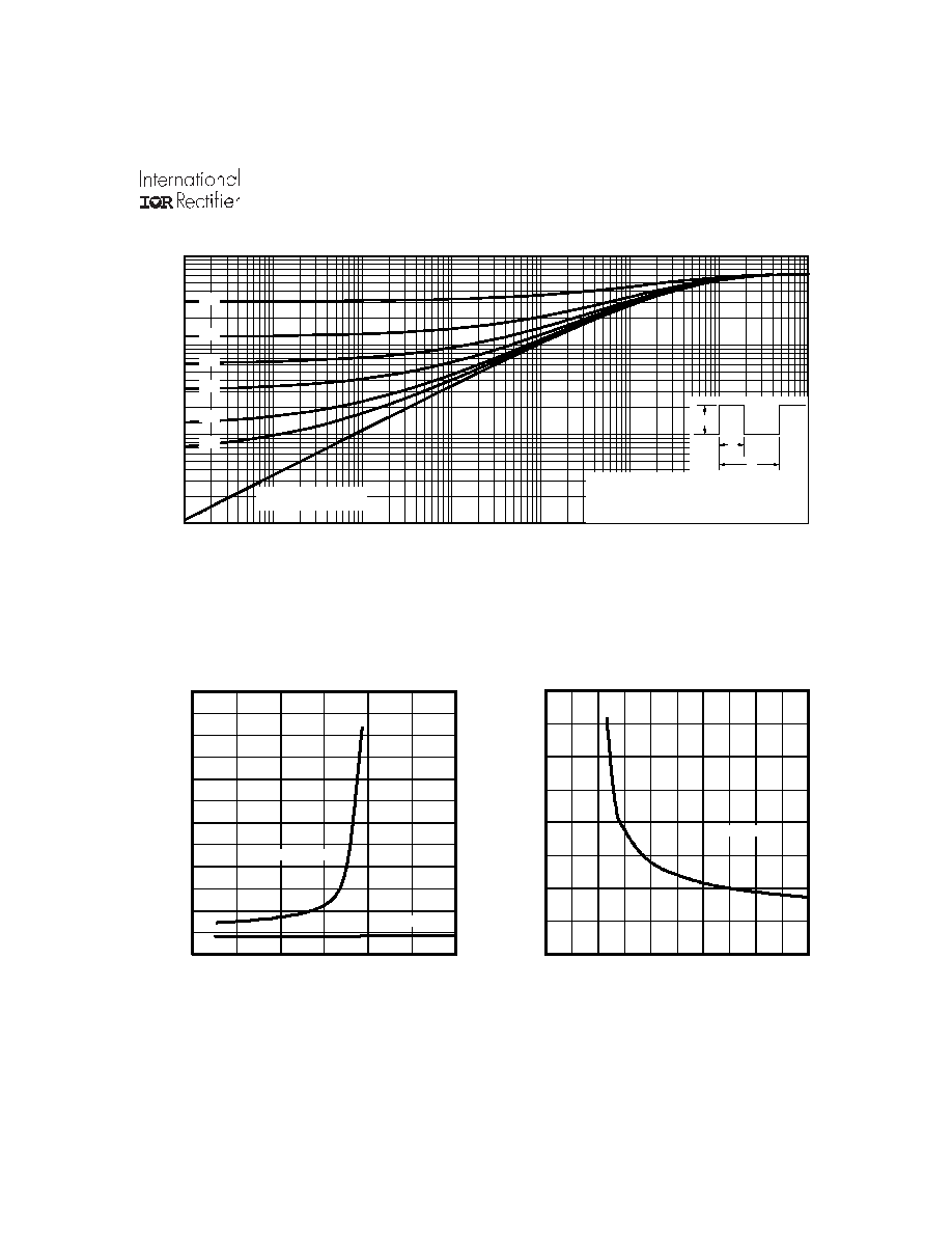
Fig 9. Maximum Effective Transient Thermal Impedance, Junction-to-Ambient
Fig 10. Typical On-Resistance Vs. Drain
Current
Fig 11. Typical On-Resistance Vs. Gate
Voltage
0.1
1
10
100
0.00001
0.0001
0.001
0.01
0.1
1
10
100
Notes:
1. Duty factor D = t / t
2. Peak T = P
x Z
+ T
1
2
J
DM
thJA
A
P
t
t
DM
1
2
t , Rectangular Pulse Duration (sec)
T
her
m
a
l
R
e
sponse
(Z
)
1
thJA
0.01
0.02
0.05
0.10
0.20
0.50
SINGLE PULSE
(THERMAL RESPONSE)
R
DS
(on)
,
Drain-to-Source
On
R
esistance
(
)
0.0
0.1
0.2
0.3
0.4
0.5
0.6
0
10
20
30
A
V = -4.5V
V = -10V
GS
GS
-I
D
, Drain Current (A)
0.00
0.04
0.08
0.12
0.16
0
3
6
9
12
15
A
I = -4.9A
D
R
DS
(on)
,
Drain-to-Source
On
Resistance
(
)
-V
GS
, Gate -to-Source Voltage (V)
Power Mosfet Characteristics