 | ÐлекÑÑоннÑй компоненÑ: IRF7353D1 | СкаÑаÑÑ:  PDF PDF  ZIP ZIP |
Äîêóìåíòàöèÿ è îïèñàíèÿ www.docs.chipfind.ru
www.irf.com
1
q
Co-packaged HEXFET
®
Power MOSFET
and Schottky Diode
q
Ideal For Buck Regulator Applications
q
N-Channel HEXFET
q
Low V
F
Schottky Rectifier
q
Generation 5 Technology
q
SO-8 Footprint
IRF7353D1
FETKY
TM
TM
TM
TM
TM
MOSFET / Schottky Diode
Parameter
Maximum
Units
R
JA
Junction-to-Ambient
62.5
°C/W
Thermal Resistance Ratings
Description
V
DSS
= 30V
R
DS(on)
= 0.029
Schottky Vf = 0.39V
The FETKY family of co-packaged MOSFETs and Schottky diodes offers the
designer an innovative, board space saving solution for switching regulator
and power management applications. Generation 5 HEXFET Power
MOSFETs utilize advanced processing techniques to achieve extremely low
on-resistance per silicon area. Combinining this technology with
International Rectifier's low forward drop Schottky rectifiers results in an
extremely efficient device suitable for use in a wide variety of portable
electronics applications.
The SO-8 has been modified through a customized leadframe for
enhanced thermal characteristics. The SO-8 package is designed for vapor
phase, infrared or wave soldering techniques.
S O -8
3/17/99
Notes:
Repetitive rating; pulse width limited by maximum junction temperature (see figure 9)
Starting T
J
= 25°C, L = 10mH, R
G
= 25
, I
AS
= 4.0A
I
SD
4.0A, di/dt
74A/µs, V
DD
V
(BR)DSS
, T
J
150°C
Pulse width
300µs; duty cycle
2%
Surface mounted on FR-4 board, t
10sec.
T op V ie w
8
1
2
3
4
5
6
7
A
A
S
G
D
D
K
K
Parameter
Maximum
Units
I
D
@ T
A
= 25°C
Continuous Drain Current
6.5
A
I
D
@ T
A
= 70°C
5.2
I
DM
Pulsed Drain Current
52
P
D
@T
A
= 25°C
Power Dissipation
2.0
W
P
D
@T
A
= 70°C
1.3
Linear Derating Factor
16
mW/°C
V
GS
Gate-to-Source Voltage
± 20
V
dv/dt
Peak Diode Recovery dv/dt
-5.0
V/ns
T
J,
T
STG
Junction and Storage Temperature Range
-55 to +150
°C
Absolute Maximum Ratings
(T
A
= 25°C unless otherwise noted)
PD- 91802A
IRF7353D1
2
www.irf.com
Parameter
Min. Typ. Max. Units
Conditions
V
(BR)DSS
Drain-to-Source Breakdown Voltage
30
--
--
V
V
GS
= 0V, I
D
= 250µA
R
DS(on)
Static Drain-to-Source On-Resistance
--
0.023 0.032
V
GS
= 10V, I
D
= 5.8A
--
0.032 0.046
V
GS
= 4.5V, I
D
= 4.7A
V
GS(th)
Gate Threshold Voltage
1.0
--
--
V
V
DS
= V
GS
, I
D
= 250µA
g
fs
Forward Transconductance
--
14
--
S
V
DS
= 24V, I
D
= 5.8A
I
DSS
Drain-to-Source Leakage Current
--
--
1.0
V
DS
= 24V, V
GS
= 0V
--
--
25
V
DS
= 24V, V
GS
= 0V, T
J
= 55°C
I
GSS
Gate-to-Source Forward Leakage
--
--
100
V
GS
= 20V
Gate-to-Source Reverse Leakage
--
--
-100
V
GS
= -20V
Q
g
Total Gate Charge
--
22
33
I
D
= 5.8A
Q
gs
Gate-to-Source Charge
--
2.6
3.9
nC
V
DS
= 24V
Q
gd
Gate-to-Drain ("Miller") Charge
--
6.4
9.6
V
GS
= 10V (see figure 8)
t
d(on)
Turn-On Delay Time
--
8.1
12
V
DD
= 15V
t
r
Rise Time
--
8.9
13
I
D
= 1.0A
t
d(off)
Turn-Off Delay Time
--
26
39
R
G
= 6.0
t
f
Fall Time
--
17
26
R
D
= 15
C
iss
Input Capacitance
--
650
--
V
GS
= 0V
C
oss
Output Capacitance
--
320
--
pF
V
DS
= 25V
C
rss
Reverse Transfer Capacitance
--
130
--
= 1.0MHz (see figure 7)
MOSFET Electrical Characteristics @ T
J
= 25°C (unless otherwise specified)
µ A
n A
ns
Parameter
Min. Typ.
Max.
Units
Conditions
I
S
Continuous Source Current (Body Diode) --
--
2.5
A
I
SM
Pulsed Source Current (Body Diode)
--
--
30
V
SD
Body Diode Forward Voltage
--
0.78
1.0
V
T
J
= 25°C, I
S
= 1.7A, V
GS
= 0V
t
rr
Reverse Recovery Time (Body Diode)
--
45
68
ns
T
J
= 25°C, I
F
= 1.7A
Q
rr
Reverse Recovery Charge
--
58
87
nC
di/dt = 100A/µs
MOSFET Source-Drain Ratings and Characteristics
Parameter
Max. Units.
Conditions
I
F(av)
Max. Average Forward Current
2.7
50% Duty Cycle. Rectangular Wave, T
A
= 25°C
1.9
T
A
= 70°C
I
SM
Max. peak one cycle Non-repetitive
120
5µs sine or 3µs Rect. pulse
Following any rated
Surge current
11
10ms sine or 6ms Rect. pulse load condition &
with V
RRM
applied
A
A
Schottky Diode Maximum Ratings
Schottky Diode Electrical Specifications
V
mA
Parameter
Max. Units
Conditions
V
FM
Max. Forward voltage drop
0.50
I
F
= 1.0A, T
J
= 25°C
0.62
I
F
= 2.0A, T
J
= 25°C
0.39
I
F
= 1.0A, T
J
= 125°C
0.57
I
F
= 2.0A, T
J
= 125°C .
I
RM
Max. Reverse Leakage current
0.06
V
R
= 30V
T
J
= 25°C
16
T
J
= 125°C
C
t
Max. Junction Capacitance
92
pF
V
R
= 5Vdc ( 100kHz to 1 MHz) 25°C
dv/dt
Max. Voltage Rate of Charge
3600 V/ µs Rated V
R
See Fig. 14
IRF7353D1
www.irf.com
3
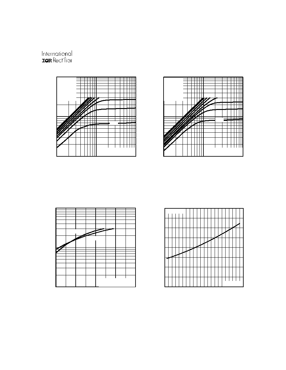
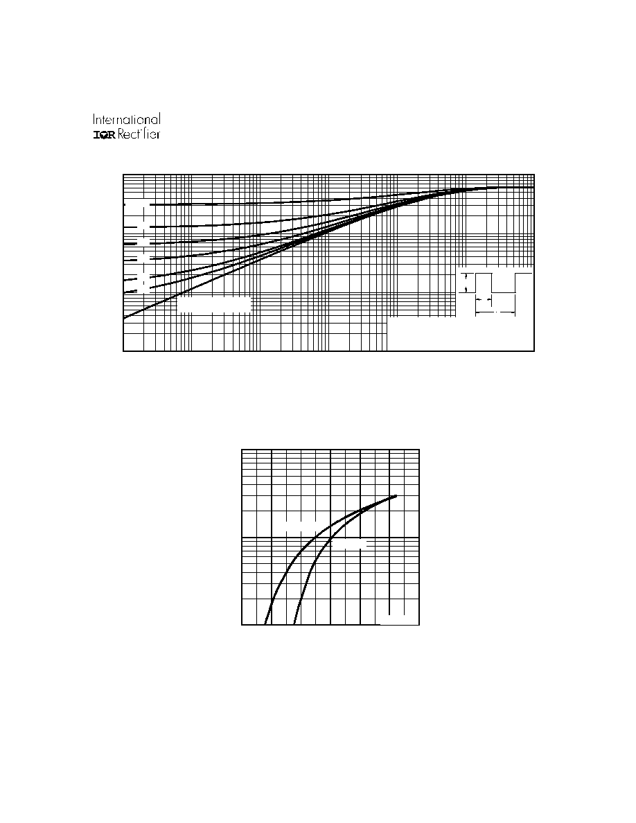
Fig 3. Typical Transfer Characteristics
Fig 2. Typical Output Characteristics
Fig 1. Typical Output Characteristics
Fig 4. Normalized On-Resistance
Vs. Temperature
Power Mosfet Characteristics
1
1 0
1 0 0
0 . 1
1
1 0
2 0 µ s P U L S E W I D T H
T = 25°C
A
J
D S
V , Drain-to-Source Voltage (V)
3.0V
VGS
TOP 15V
10V
7.0V
5.5V
4.5V
4.0V
3.5V
BOTTOM 3.0V
DI , Drain-to-Source Current (A)
1
1 0
1 0 0
0 . 1
1
1 0
A
D S
V , Drain-to-Source Voltage (V)
DI , Drain-to-Source Current (A)
2 0 µ s P U L S E W I D T H
T = 150°C
J
3.0V
VGS
TOP 15V
10V
7.0V
5.5V
4.5V
4.0V
3.5V
BOTTOM 3.0V
1
1 0
1 0 0
3 . 0
3 . 5
4 . 0
4 . 5
5 . 0
T = 25°C
T = 150°C
J
J
G S
V , Gate-to-Source Voltage (V)
D
I , Drain-to-Source Current (A)
A
V = 10V
20µs PULSE WIDTH
D S
-60 -40 -20
0
20
40
60
80 100 120 140 160
0.0
0.5
1.0
1.5
2.0
T , Junction Temperature ( C)
R , Drain-to-Source On Resistance
(Normalized)
J
DS(on)
°
V
=
I =
GS
D
10V
5.8A
IRF7353D1
4
www.irf.com
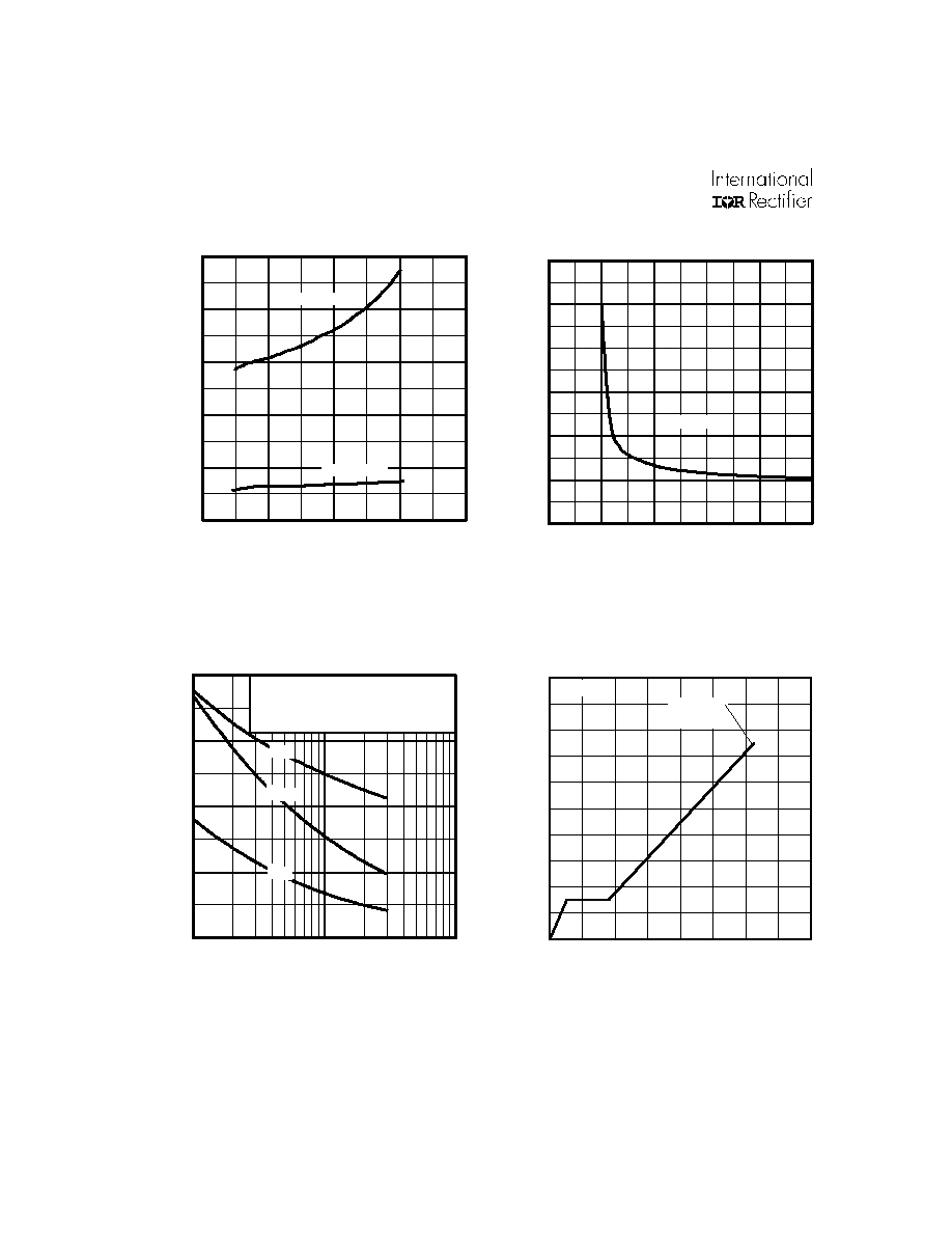
Power Mosfet Characteristics
Fig 5. Typical On-Resistance Vs. Drain
Current
Fig 6. Typical On-Resistance Vs. Gate
Voltage
R
DS
(on) , Drain-to-Source On Resistance (
)
0 . 0 2 0
0 . 0 2 4
0 . 0 2 8
0 . 0 3 2
0 . 0 3 6
0 . 0 4 0
0
1 0
2 0
3 0
4 0
A
I , Drain Current (A)
D
V = 10V
G S
V = 4.5V
G S
R
DS
(on) , Drain-to-Source On Resistance (
)
0 . 0 0
0 . 0 2
0 . 0 4
0 . 0 6
0 . 0 8
0 . 1 0
0 . 1 2
0
3
6
9
1 2
1 5
A
G S
V , Gate-to-Source Voltage (V)
I = 5.8A
D
Fig 8. Typical Gate Charge Vs.
Gate-to-Source Voltage
Fig 7. Typical Capacitance Vs.
Drain-to-Source Voltage
0
3 0 0
6 0 0
9 0 0
1 2 0 0
1
1 0
1 0 0
C
,
Cap
ac
i
t
a
n
c
e
(
p
F
)
D S
V , D rain-to-S ourc e V oltage (V )
A
V = 0V , f = 1M H z
C = C + C , C S H O R T E D
C = C
C = C + C
G S
is s g s g d d s
rs s g d
o ss d s gd
C
is s
C
os s
C
rs s
0
10
20
30
40
0
4
8
12
16
20
Q , Total Gate Charge (nC)
V , Gate-to-Source Voltage (V)
G
GS
I =
D
5.8A
V
= 15V
DS
IRF7353D1
www.irf.com
5
0.1
1
10
100
0.0001
0.001
0.01
0.1
1
10
100
Notes:
1. Duty factor D =
t / t
2. Peak T = P
x Z
+ T
1
2
J
DM
thJA
A
P
t
t
DM
1
2
t , Rectangular Pulse Duration (sec)
Thermal Response
(Z )
1
thJA
0.01
0.02
0.05
0.10
0.20
D = 0.50
SINGLE PULSE
(THERMAL RESPONSE)
Fig 9. Maximum Effective Transient Thermal Impedance, Junction-to-Ambient
Power Mosfet Characteristics
Fig 10. Typical Source-Drain Diode
Forward Voltage
1
1 0
1 0 0
0 . 4
0 . 6
0 . 8
1 . 0
1 . 2
1 . 4
1 . 6
T = 25°C
T = 1 5 0 ° C
J
J
V = 0V
G S
V , Source-to-Drain Voltage (V)
I , Reverse Drain Current (A)
S D
SD
A