
www.irf.com
1
7/29/03
SO-8
Top View
8
1
2
3
4
5
6
7
D
D
D
D
G
S
A
S
S
A
IRF7493
HEXFET
�
Power MOSFET
Notes
through
are on page 9
PD - 94654B
l
High frequency DC-DC converters
Benefits
Applications
l
Low Gate-to-Drain Charge to Reduce
Switching Losses
l
Fully Characterized Capacitance Including
Effective C
OSS
to Simplify Design, (See
App. Note AN1001)
l
Fully Characterized Avalanche Voltage
and Current
V
DSS
R
DS(on)
max
Qg (typ.)
80V
15m
:
@V
GS
=10V
35nC
Absolute Maximum Ratings
Parameter
Units
V
DS
Drain-to-Source Voltage
V
V
GS
Gate-to-Source Voltage
I
D
@ T
C
= 25�C
Continuous Drain Current, V
GS
@ 10V
I
D
@ T
C
= 70�C
Continuous Drain Current, V
GS
@ 10V
A
I
DM
Pulsed Drain Current
c
P
D
@T
C
= 25�C
Maximum Power Dissipation
f
W
P
D
@T
C
= 70�C
Maximum Power Dissipation
f
Linear Derating Factor
W/�C
T
J
Operating Junction and
�C
T
STG
Storage Temperature Range
Thermal Resistance
Parameter
Typ.
Max.
Units
R
JC
Junction-to-Lead
���
20
R
JA
Junction-to-Ambient
f
���
50
Max.
9.3
7.4
74
� 20
80
-55 to + 150
2.5
0.02
1.6

IRF7493
2
www.irf.com
Static @ T
J
= 25�C (unless otherwise specified)
Parameter
Min. Typ. Max. Units
BV
DSS
Drain-to-Source Breakdown Voltage
80
���
���
V
V
DSS
/
T
J
Breakdown Voltage Temp. Coefficient
���
0.074
���
mV/�C
R
DS(on)
Static Drain-to-Source On-Resistance
���
11.5
15
m
V
GS(th)
Gate Threshold Voltage
2.0
���
4.0
V
I
DSS
Drain-to-Source Leakage Current
���
���
20
�A
���
���
250
I
GSS
Gate-to-Source Forward Leakage
���
���
200
nA
Gate-to-Source Reverse Leakage
���
���
-200
Dynamic @ T
J
= 25�C (unless otherwise specified)
gfs
Forward Transconductance
13
���
���
S
Q
g
Total Gate Charge
���
35
53
Q
gs
Gate-to-Source Charge
���
5.7
���
Q
gd
Gate-to-Drain Charge
���
12
���
t
d(on)
Turn-On Delay Time
���
8.3
���
t
r
Rise Time
���
7.5
���
t
d(off)
Turn-Off Delay Time
���
30
���
ns
t
f
Fall Time
���
12
���
C
iss
Input Capacitance
���
1510
���
C
oss
Output Capacitance
���
320
���
pF
C
rss
Reverse Transfer Capacitance
���
130
���
C
oss
Output Capacitance
���
1130
���
C
oss
Output Capacitance
���
210
���
C
rss
eff.
Effective Output Capacitance
���
320
���
Avalanche Characteristics
Parameter
Units
E
AS
Single Pulse Avalanche Energy
d
mJ
I
AR
Avalanche Current
�
A
Diode Characteristics
Parameter
Min. Typ. Max. Units
I
S
Continuous Source Current
���
���
9.3
(Body Diode)
A
I
SM
Pulsed Source Current
���
���
74
(Body Diode)
�
V
SD
Diode Forward Voltage
���
���
1.3
V
t
rr
Reverse Recovery Time
���
37
56
ns
Q
rr
Reverse Recovery Charge
���
52
78
nC
R
G
= 6.2
Conditions
V
GS
= 10V
Max.
180
5.6
V
GS
= 0V, V
DS
= 0V to 64V
g
Conditions
V
GS
= 0V, I
D
= 250�A
Reference to 25�C, I
D
= 1mA
V
GS
= 10V, I
D
= 5.6A
e
T
J
= 25�C, I
F
= 5.6A, V
DD
= 15V
di/dt = 100A/�s
e
T
J
= 25�C, I
S
= 5.6A, V
GS
= 0V
e
showing the
integral reverse
p-n junction diode.
Typ.
���
���
V
GS
= 10V
V
GS
= 0V
V
DS
= 25V
V
GS
= 0V, V
DS
= 1.0V, = 1.0MHz
V
GS
= 0V, V
DS
= 64V, = 1.0MHz
V
DD
= 40V,
e
I
D
= 5.6A
MOSFET symbol
V
DS
= V
GS
, I
D
= 250�A
V
DS
= 80V, V
GS
= 0V
V
DS
= 64V, V
GS
= 0V, T
J
= 125�C
= 1.0MHz
V
DS
= 15V, I
D
= 5.6A
V
DS
= 40V
V
GS
= 20V
V
GS
= -20V
I
D
= 5.6A
IRF7493
www.irf.com
3
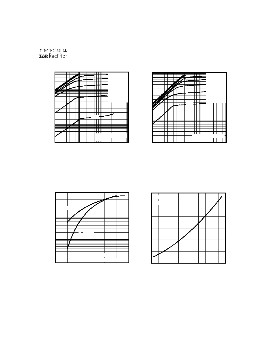
Fig 2. Typical Output Characteristics
Fig 1. Typical Output Characteristics
Fig 3. Typical Transfer Characteristics
Fig 4. Normalized On-Resistance
Vs. Temperature
0.1
1
10
100
VDS, Drain-to-Source Voltage (V)
0.01
0.1
1
10
100
I D
,
D
r
a
i
n
-
t
o
-
S
o
u
r
c
e
C
u
r
r
e
n
t
(
A
)
3.5V
20�s PULSE WIDTH
Tj = 25�C
0.1
1
10
100
VDS, Drain-to-Source Voltage (V)
0.1
1
10
100
I D
,
D
r
a
i
n
-
t
o
-
S
o
u
r
c
e
C
u
r
r
e
n
t
(
A
)
3.5V
20�s PULSE WIDTH
Tj = 150�C
V
GS
TOP 15V
10V
8.0V
5.5V
5.0V
4.5V
4.0V
BOTTOM 3.5V
V
GS
TOP 15V
10V
8.0V
5.5V
5.0V
4.5V
4.0V
BOTTOM 3.5V
3.0
4.0
5.0
6.0
VGS, Gate-to-Source Voltage (V)
0.10
1.00
10.00
100.00
I D
,
D
r
a
i
n
-
t
o
-
S
o
u
r
c
e
C
u
r
r
e
n
t
(
)
TJ = 25�C
TJ = 150�C
VDS = 25V
20�s PULSE WIDTH
-60 -40 -20
0
20
40
60
80 100 120 140 160
TJ , Junction Temperature (�C)
0.5
1.0
1.5
2.0
R
D
S
(
o
n
)
,
D
r
a
i
n
-
t
o
-
S
o
u
r
c
e
O
n
R
e
s
i
s
t
a
n
c
e
(
N
o
r
m
a
l
i
z
e
d
)
ID = 9.3A
VGS = 10V
IRF7493
4
www.irf.com
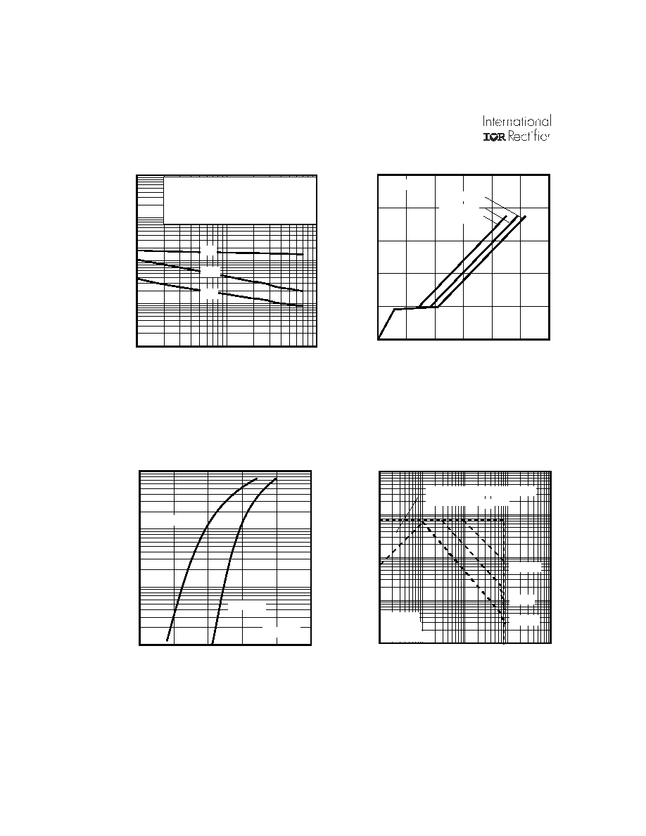
Fig 6. Typical Gate Charge Vs.
Gate-to-Source Voltage
Fig 5. Typical Capacitance Vs.
Drain-to-Source Voltage
Fig 7. Typical Source-Drain Diode
Forward Voltage
Fig 8. Maximum Safe Operating Area
1
10
100
VDS, Drain-to-Source Voltage (V)
10
100
1000
10000
100000
C
,
C
a
p
a
c
i
t
a
n
c
e
(
p
F
)
Coss
Crss
Ciss
VGS = 0V, f = 1 MHZ
Ciss = C gs + Cgd, C ds SHORTED
Crss = C gd
Coss = Cds + Cgd
0
10
20
30
40
50
60
QG Total Gate Charge (nC)
0
4
8
12
16
20
V
G
S
,
G
a
t
e
-
t
o
-
S
o
u
r
c
e
V
o
l
t
a
g
e
(
V
)
VDS= 64V
VDS= 40V
VDS= 16V
ID= 5.6A
0.2
0.4
0.6
0.8
1.0
1.2
VSD, Source-toDrain Voltage (V)
0.1
1.0
10.0
100.0
I S
D
,
R
e
v
e
r
s
e
D
r
a
i
n
C
u
r
r
e
n
t
(
A
)
TJ = 25�C
TJ = 150�C
VGS = 0V
0
1
10
100
1000
VDS , Drain-toSource Voltage (V)
0.1
1
10
100
1000
I D
,
D
r
a
i
n
-
t
o
-
S
o
u
r
c
e
C
u
r
r
e
n
t
(
A
)
Tc = 25�C
Tj = 150�C
Single Pulse
1msec
10msec
OPERATION IN THIS AREA
LIMITED BY RDS(on)
100�sec

IRF7493
www.irf.com
5
Fig 11. Maximum Effective Transient Thermal Impedance, Junction-to-Ambient
Fig 10a. Switching Time Test Circuit
V
DS
90%
10%
V
GS
t
d(on)
t
r
t
d(off)
t
f
Fig 10b. Switching Time Waveforms
V
DS
Pulse Width 1 �s
Duty Factor 0.1 %
R
D
V
GS
R
G
D.U.T.
10V
+
-
V
DD
Fig 9. Maximum Drain Current Vs.
Ambient Temperature
25
50
75
100
125
150
TC , Case Temperature (�C)
0
2
4
6
8
10
I D
,
D
r
a
i
n
C
u
r
r
e
n
t
(
A
)
1E-005
0.0001
0.001
0.01
0.1
1
10
100
t1 , Rectangular Pulse Duration (sec)
0.01
0.1
1
10
100
T
h
e
r
m
a
l
R
e
s
p
o
n
s
e
(
Z
t
h
J
C
)
0.20
0.10
D = 0.50
0.02
0.01
0.05
SINGLE PULSE
( THERMAL RESPONSE )