 | ÐлекÑÑоннÑй компоненÑ: IRF7756 | СкаÑаÑÑ:  PDF PDF  ZIP ZIP |
Äîêóìåíòàöèÿ è îïèñàíèÿ www.docs.chipfind.ru
HEXFET
®
Power MOSFET
3/17/04
IRF7756
Absolute Maximum Ratings
www.irf.com
1
Thermal Resistance
Parameter
Max.
Units
V
DS
Drain-Source Voltage
-12
V
I
D
@ T
A
= 25°C
Continuous Drain Current, V
GS
@ -4.5V
-4.3
I
D
@ T
A
= 70°C
Continuous Drain Current, V
GS
@ -4.5V
-3.5
A
I
DM
Pulsed Drain Current
-17
P
D
@T
A
= 25°C
Maximum Power Dissipation
1.0
W
P
D
@T
A
= 70°C
Maximum Power Dissipation
0.64
W
Linear Derating Factor 8.0 mW/°C
V
GS
Gate-to-Source Voltage
±8.0 V
T
J
, T
STG
Junction and Storage Temperature Range
-55 to +150
°C
V
DSS
R
DS(on)
max
I
D
-12V
0.040@V
GS
= -4.5V
±
4.3A
0.058@V
GS
= -2.5V
±
3.4A
0.087@V
GS
= -1.8V
±
2.2A
Parameter
Max.
Units
R
JA
Maximum Junction-to-Ambient
125
°C/W
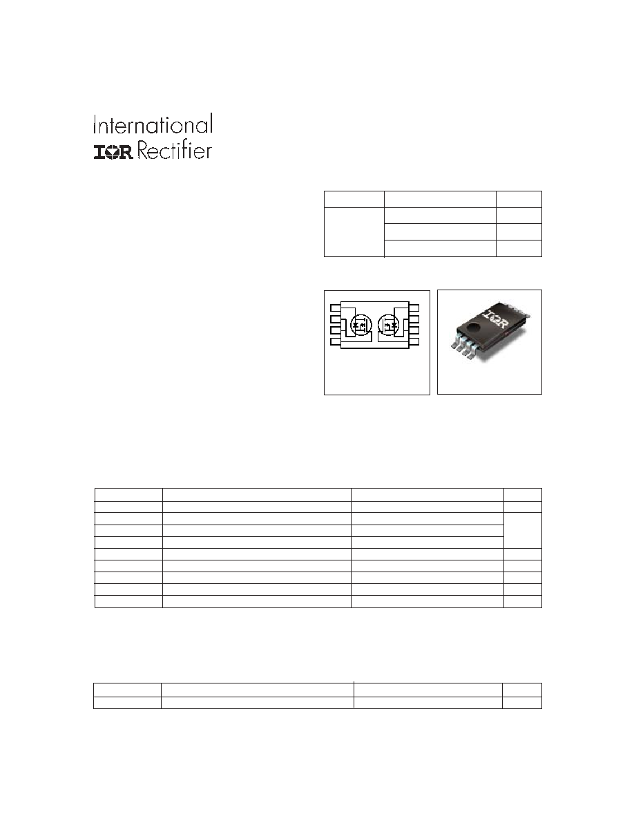
TSSOP-8
Description
HEXFET
®
Power MOSFETs from International Rectifier
utilize advanced processing techniques to achieve ex-
tremely low on-resistance per silicon area. This benefit,
combined with the ruggedized device design, that Inter-
national Rectifier is well known for,
provides thedesigner
with an extremely efficient and reliable device for
battery and load management.
The TSSOP-8 package has 45% less footprint area than
the standard SO-8. This makes the TSSOP-8 an ideal
device for applications where printed circuit board space
is at a premium. The low profile (<1.1mm) allows it to fit
easily into extremely thin environments such as portable
electronics and PCMCIA cards.
4 = G1
3 = S1
2 = S1
1 = D1
1
2
3
4
5
6
7
8
5 = G2
6 = S 2
7 = S2
8 = D2
l
Ultra Low On-Resistance
l
Dual P-Channel MOSFET
l
Very Small SOIC Package
l
Low Profile (< 1.2mm)
l
Available in Tape & Reel
PD -94159A
IRF7756
2
www.irf.com
Parameter
Min. Typ. Max. Units
Conditions
I
S
Continuous Source Current
MOSFET symbol
(Body Diode)
showing the
I
SM
Pulsed Source Current
integral reverse
(Body Diode)
p-n junction diode.
V
SD
Diode Forward Voltage
-1.2
V
T
J
= 25°C, I
S
= -1.0A, V
GS
= 0V
t
rr
Reverse Recovery Time
35
53
ns
T
J
= 25°C, I
F
= -1.0A
Q
rr
Reverse Recovery Charge
20
30
nC
di/dt = -100A/µs
Source-Drain Ratings and Characteristics
-17
-1.0
A
Electrical Characteristics @ T
J
= 25°C (unless otherwise specified)
Notes:
Repetitive rating; pulse width limited by
max. junction temperature.
Pulse width
400µs
;
duty cycle
2%.
Surface mounted on FR-4 board,
t
10sec
.
S
D
G
Parameter
Min. Typ. Max. Units
Conditions
V
(BR)DSS
Drain-to-Source Breakdown Voltage
-12
V
V
GS
= 0V, I
D
= -250µA
V
(BR)DSS
/
T
J
Breakdown Voltage Temp. Coefficient
-0.006
V/°C
Reference to 25°C, I
D
= -1mA
0.040
V
GS
= -4.5V, I
D
= -4.3A
0.058
V
GS
= -2.5V, I
D
= -3.4A
0.087
V
GS
= -1.8V, I
D
= -2.2A
V
GS(th)
Gate Threshold Voltage
-0.4
-0.9
V
V
DS
= V
GS
, I
D
= -250µA
g
fs
Forward Transconductance
13
S
V
DS
= -10V, I
D
= -4.3A
-1.0
V
DS
= -9.6V, V
GS
= 0V
-25
V
DS
= -9.6V, V
GS
= 0V, T
J
= 70°C
Gate-to-Source Forward Leakage
-100
V
GS
= -8.0V
Gate-to-Source Reverse Leakage
100
V
GS
= 8.0V
Q
g
Total Gate Charge
12
18
I
D
= -4.3A
Q
gs
Gate-to-Source Charge
1.8
2.7
nC
V
DS
= -6.0V
Q
gd
Gate-to-Drain ("Miller") Charge
2.9
4.4
V
GS
= -4.5V
t
d(on)
Turn-On Delay Time
12
V
DD
= -6.0V,
t
r
Rise Time
18
I
D
= -1.0A
t
d(off)
Turn-Off Delay Time
160
R
G
= 6.0
t
f
Fall Time
170
V
GS
= -4.5V
C
iss
Input Capacitance
1400
V
GS
= 0V
C
oss
Output Capacitance
310
pF
V
DS
= -10V
C
rss
Reverse Transfer Capacitance
240
= 1.0kHz
I
GSS
µA
R
DS(on)
Static Drain-to-Source On-Resistance
I
DSS
Drain-to-Source Leakage Current
nA
ns
IRF7756
www.irf.com
3
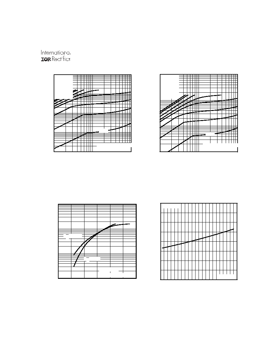
Fig 3. Typical Transfer Characteristics
Fig 2. Typical Output Characteristics
Fig 1. Typical Output Characteristics
0.01
0.1
1
10
100
0.1
1
10
20µs PULSE WIDTH
T = 25 C
J
°
TOP
BOTTOM
VGS
-7.5V
-4.5V
-2.5V
-1.8V
-1.5V
-1.2V
-1.0V
-0.8V
-V , Drain-to-Source Voltage (V)
-I , Drain-to-Source Current (A)
DS
D
-0.8V
0.1
1
10
100
0.1
1
10
20µs PULSE WIDTH
T = 150 C
J
°
TOP
BOTTOM
VGS
-7.5V
-4.5V
-2.5V
-1.8V
-1.5V
-1.2V
-1.0V
-0.8V
-V , Drain-to-Source Voltage (V)
-
I
,
Dr
ai
n-
t
o
-
S
our
ce Cur
r
ent
(
A
)
DS
D
-0.8V
Fig 4. Normalized On-Resistance
Vs. Temperature
0.5
1.0
1.5
2.0
-VGS, Gate-to-Source Voltage (V)
0
1
10
100
-
I D
,
D
r
a
i
n
-
t
o
-
S
o
u
r
c
e
C
u
r
r
e
n
t
(
)
TJ = 25°C
TJ = 150°C
VDS = -10V
20µs PULSE WIDTH
-60 -40 -20
0
20
40
60
80 100 120 140 160
0.0
0.5
1.0
1.5
2.0
T , Junction Temperature( C)
R , Drain-to-Source On Resistance
(Normalized)
J
DS
(
on)
°
V
=
I =
GS
D
-4.5V
-4.3A
IRF7756
4
www.irf.com
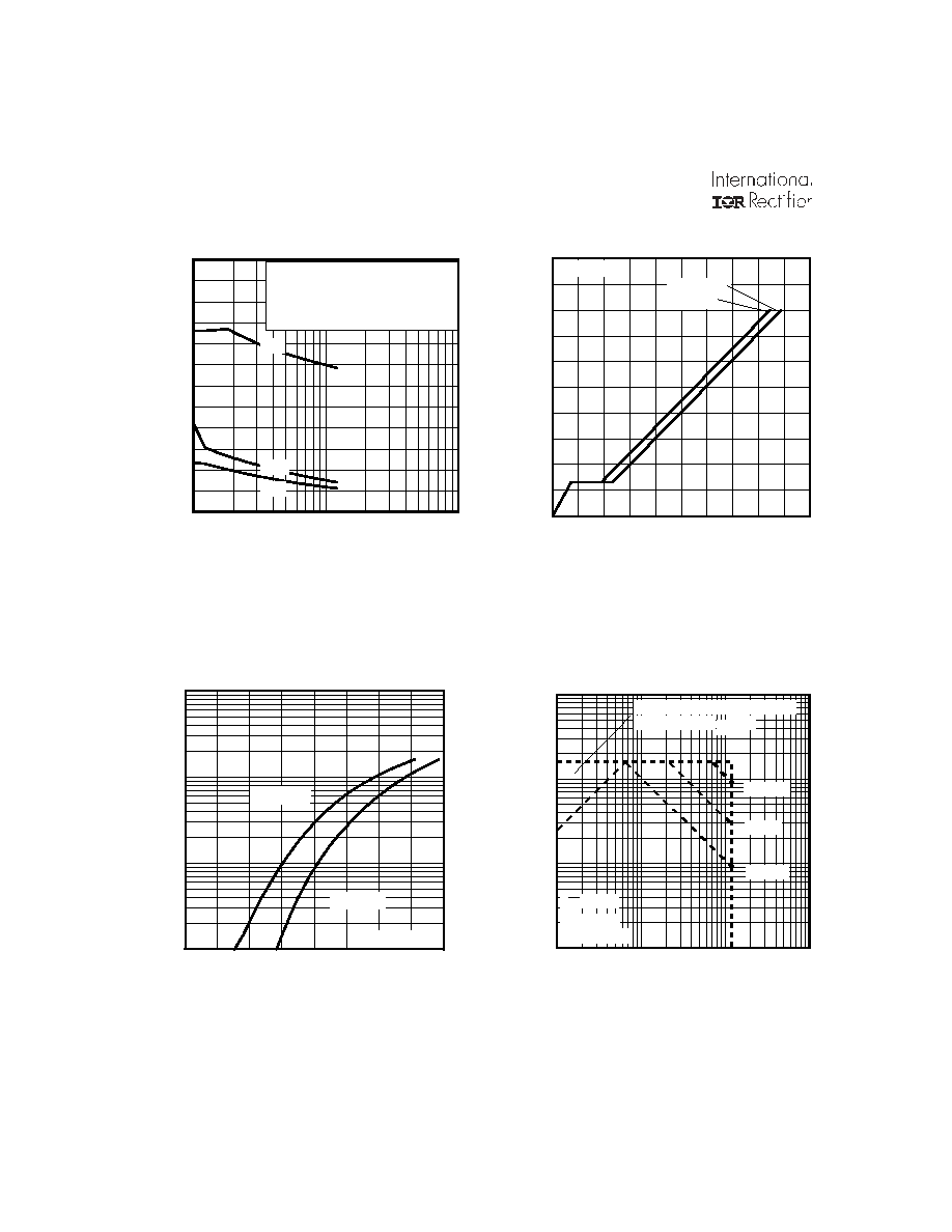
Fig 6. Typical Gate Charge Vs.
Gate-to-Source Voltage
Fig 5. Typical Capacitance Vs.
Drain-to-Source Voltage
Fig 8. Maximum Safe Operating Area
0
5
10
15
20
25
0
2
4
6
8
10
Q , Total Gate Charge (nC)
-V , G
a
te-to-Source Voltage (V)
G
GS
I =
D
-4.3A
V
=-6V
DS
V
=-9.6V
DS
Fig 7. Typical Source-Drain Diode
Forward Voltage
1
10
100
-VDS, Drain-to-Source Voltage (V)
0
400
800
1200
1600
2000
2400
C
,
C
a
p
a
c
i
t
a
n
c
e
(
p
F
)
Coss
Crss
Ciss
VGS = 0V, f = 1 MHZ
Ciss = Cgs + Cgd, Cds SHORTED
Crss = Cgd
Coss = Cds + Cgd
0.1
1
10
100
-VDS , Drain-toSource Voltage (V)
0.1
1
10
100
-
I D
,
D
r
a
i
n
-
t
o
-
S
o
u
r
c
e
C
u
r
r
e
n
t
(
A
)
TA = 25°C
Tj = 150°C
Single Pulse
1msec
10msec
OPERATION IN THIS AREA
LIMITED BY RDS(on)
100µsec
0.1
1
10
100
0.2
0.4
0.6
0.8
1.0
-V ,Source-to-Drain Voltage (V)
-I , Reverse Drain Current (A)
SD
SD
V = 0 V
GS
T = 25 C
J
°
T = 150 C
J
°
IRF7756
www.irf.com
5
Fig 10. Typical Effective Transient Thermal Impedance, Junction-to-Ambient
Fig 9. Maximum Drain Current Vs.
Case Temperature
25
50
75
100
125
150
0.0
1.0
2.0
3.0
4.0
5.0
T , Case Temperature ( C)
-
I
,
Dr
ai
n Cur
r
ent
(
A
)
°
C
D
0.1
1
10
100
1000
0.00001
0.0001
0.001
0.01
0.1
1
10
100
Notes:
1. Duty factor D = t / t
2. Peak T = P
x Z
+ T
1
2
J
DM
thJA
A
P
t
t
DM
1
2
t , Rectangular Pulse Duration (sec)
Thermal Res
pons
e
(
Z
)
1
thJA
0.01
0.02
0.05
0.10
0.20
D = 0.50
SINGLE PULSE
(THERMAL RESPONSE)
V
DS
V
GS
Pulse Width 1 µs
Duty Factor 0.1 %
R
D
V
GS
V
DD
R
G
D.U.T.
+
-
V
DS
90%
10%
V
GS
t
d(on)
t
r
t
d(off)
t
f
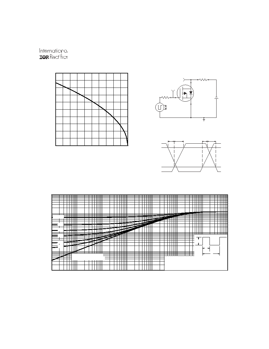
Fig 10a. Switching Time Test Circuit
Fig 10b. Switching Time Waveforms