 | ÐлекÑÑоннÑй компоненÑ: IRF7807D1 | СкаÑаÑÑ:  PDF PDF  ZIP ZIP |
Äîêóìåíòàöèÿ è îïèñàíèÿ www.docs.chipfind.ru
Parameter
Symbol
Max.
Units
Drain-Source Voltage
V
DS
30
Gate-Source Voltage
V
GS
±12
Continuous Drain or Source
25°C
I
D
8.3
Current (V
GS
4.5V)
70°C
6.6
A
Pulsed Drain Current
I
DM
66
Power Dissipation
25°C
P
D
2.5
70°C
1.6
Schottky and Body Diode
25°C
I
F
(AV)
3.5
A
Average ForwardCurrent
70°C
2.2
Junction & Storage Temperature Range
T
J
,
T
STG
55 to 150
°C
· Co-Pack N-channel HEXFET
®
Power MOSFET
and Schottky Diode
· Ideal for Synchronous Rectifiers in DC-DC
Converters Up to 5A Output
· Low Conduction Losses
· Low Switching Losses
· Low Vf Schottky Rectifier
FETKYTM MOSFET / SCHOTTKY DIODE
Absolute Maximum Ratings
Parameter
Max.
Units
Maximum Junction-to-Ambient
R
JA
50
°C/W
Thermal Resistance
V
W
Description
The FETKY
TM
family of Co-Pack HEXFET
®
MOSFETs and
Schottky diodes offers the designer an innovative, board
space saving solution for switching regulator and power
management applications. HEXFET power MOSFETs
utilize advanced processing techniques to achieve
extremely low on-resistance per silicon area. Combining
this technology with International Rectifier's low forward
drop Schottky rectifiers results in an extremely efficient
device suitable for use in a wide variety of portable
electronics applications.
The SO-8 has been modified through a customized
leadframe for enhanced thermal characteristics. The SO-
8 package is designed for vapor phase, infrared or wave
soldering techniques.
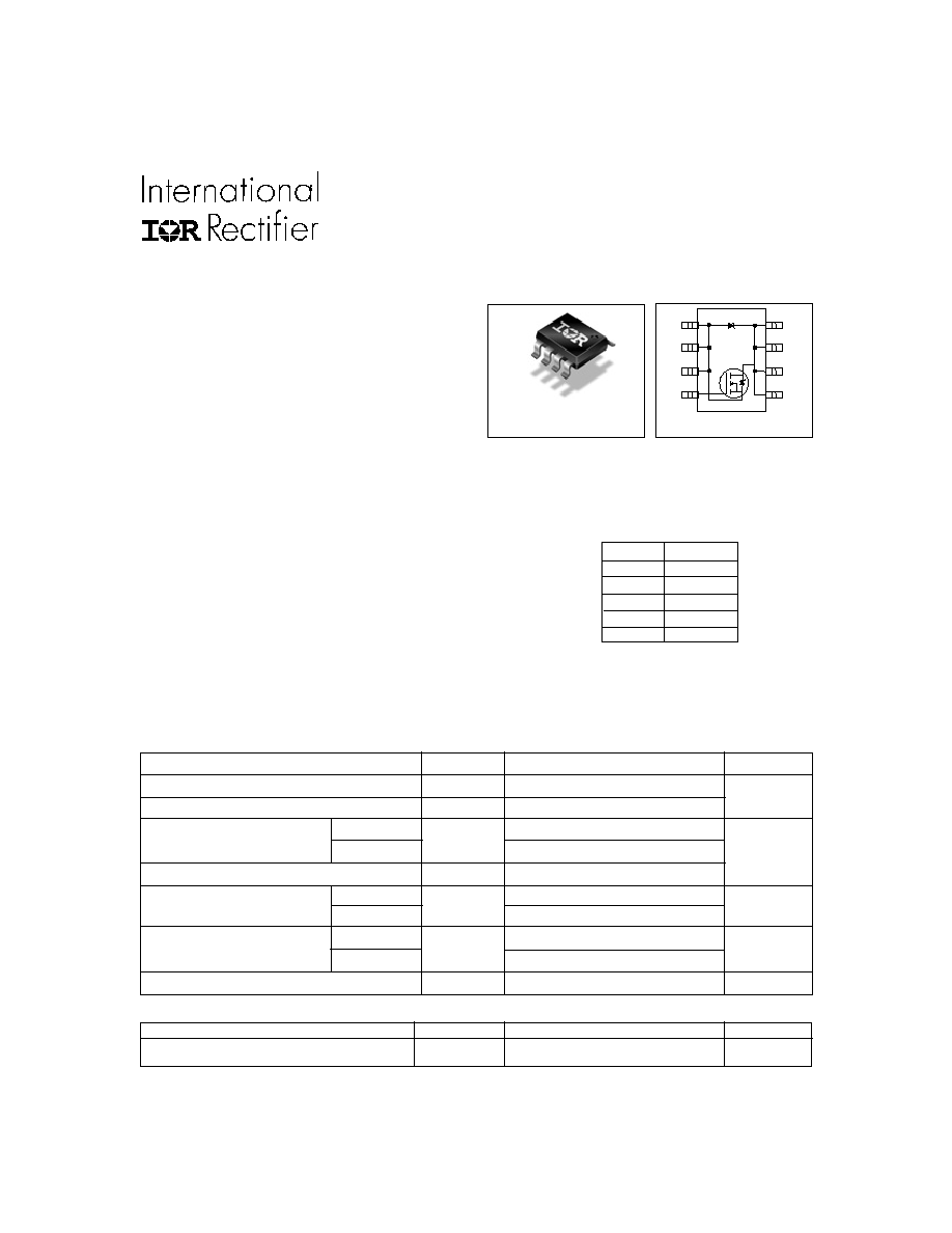
Top View
8
1
2
3
4
5
6
7
A/S
A/S
A/S
G
K/D
K/D
D
K/D
K/D
IRF7807D1
PD- 93761
www.irf.com
1
11/8/99
IRF7807D1
V
DS
30V
R
DS(on)
25m
Q
g
14nC
Q
sw
5.2nC
Q
oss
18.4nC
Device Features (Max Values)
SO-8
IRF7807D1
2
www.irf.com
Electrical Characteristics
Schottky Diode & Body Diode Ratings and Characteristics
Repetitive rating; pulse width limited by max. junction temperature.
Pulse width
300 µs; duty cycle
2%.
When mounted on 1 inch square copper board, t < 10 sec.
50% Duty Cycle, Rectangular
*
Devices are 100% tested to these parameters.
Parameter
Min
Typ
Max
Units
Conditions
Diode Forward Voltage
V
SD
0.5
V
T
j
= 25°C, I
s
= 1A, V
GS
=0V
0.39
T
j
= 125°C, I
s
= 1A, V
GS
=0V
Reverse Recovery Time
trr
51
ns
T
j
= 25°C, I
s
= 7.0A, V
DS
= 16V
Reverse Recovery Charge
Qrr
48
nC
di/dt = 100A/µs
Forward Turn-On Time
t
on
Intrinsic turn-on time is negligible (turn-on is dominated by L
S
+L
D
)
Parameter
Min
Typ
Max
Units
Conditions
Drain-to-Source
V
(BR)DSS
30
V
V
GS
= 0V, I
D
= 250µA
Breakdown Voltage*
Static Drain-Source
R
DS
(on)
17
25
m
V
GS
= 4.5V, I
D
= 7A
on Resistance*
Gate Threshold Voltage* V
GS
(th)
1.0
V
V
DS
= V
GS
,I
D
= 250µA
Drain-Source Leakage
I
DSS
90
µ
A
V
DS
= 24V, V
GS
= 0V
Current*
7.2
mA
V
DS
= 24V, V
GS
= 0V,
T
j
= 125°C
Gate-Source Leakage
I
GSS
+/- 100
nA
V
GS
= +/-12V
Current*
Total Gate Charge
Q
gsync
10.5
14
V
DS
<100mV,
Synch FET*
V
GS
= 5V, I
D
= 7A
Total Gate Charge
Q
gcont
12
17
V
DS
= 16V,
Control FET*
V
GS
= 5V, I
D
= 7A
Pre-Vth
Q
gs1
2.1
V
DS
= 16V, I
D
= 7A
Gate-Source Charge
Post-Vth
Q
gs2
0.76
nC
Gate-Source Charge
Gate to Drain Charge
Q
gd
2.9
Switch Charge*
Q
SW
3.66
5.2
(Q
gs2
+ Q
gd
)
Output Charge*
Q
oss
15.3
18.4
V
DS
= 16V, V
GS
= 0
Gate Resistance
R
g
1.2
IRF7807D1
www.irf.com
3
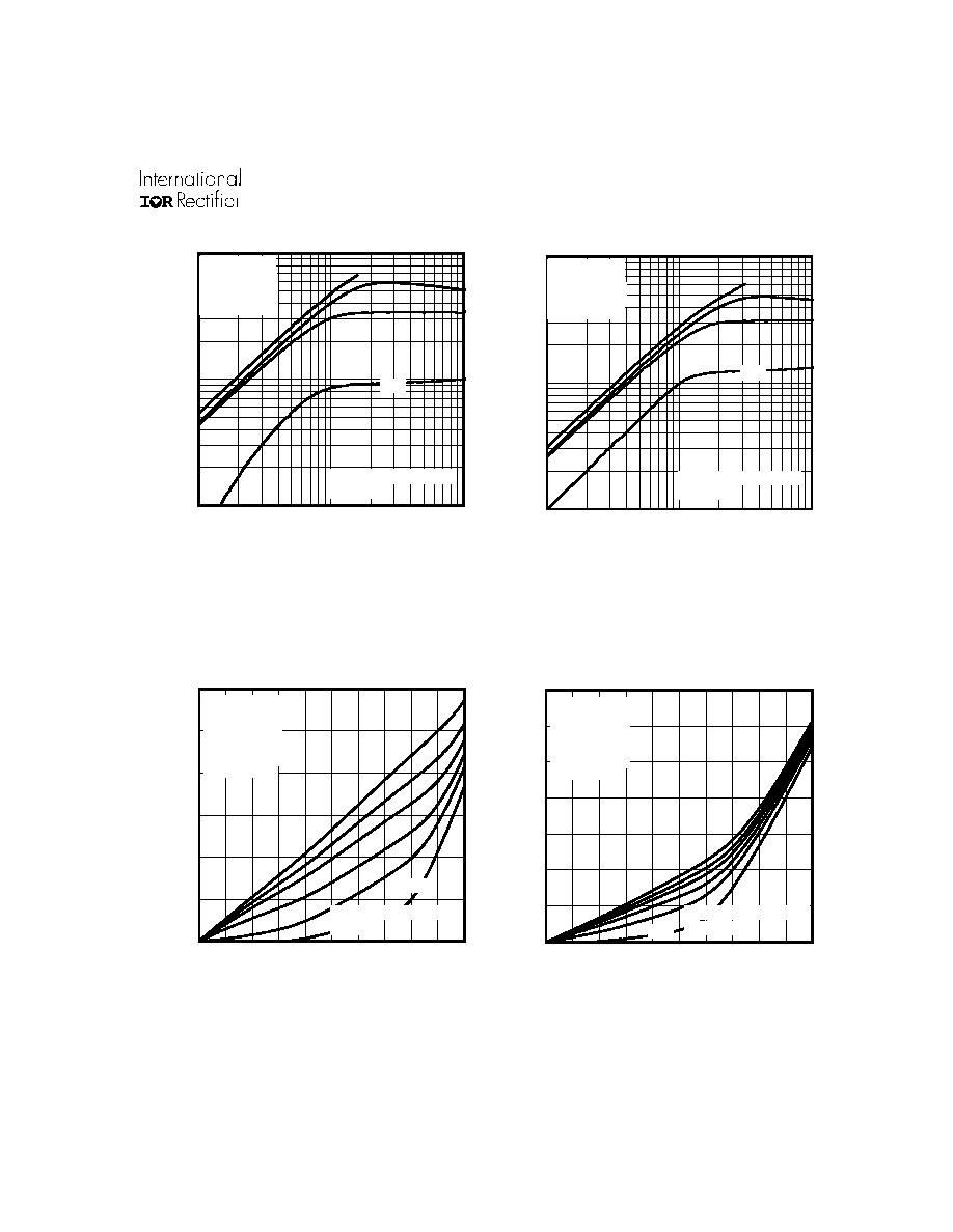
Fig 3. Typical Reverse Output Characteristics
Fig 4. Typical Reverse Output Characteristics
Fig 2. Typical Output Characteristics
Fig 1. Typical Output Characteristics
0.1
1
10
VDS, Drain-to-Source Voltage (V)
1
10
100
I D
, Drain-to-Source Current ( A )
2.5V
VGS
TOP 4.5V
3.5V
3.0V
BOTTOM 2.5V
380µs PULSE WIDTH
Tj = 25°C
0.1
1
10
VDS, Drain-to-Source Voltage (V)
1
10
100
I D
, Drain-to-Source Current (A)
2.5V
VGS
TOP 4.5V
3.5V
3.0V
BOTTOM 2.5V
380µs PULSE WIDTH
Tj = 150°C
0
0.2
0.4
0.6
0.8
1
VSD, Source-to-Drain Voltage (V)
0
10
20
30
40
50
60
I S
, Source-to-Drain Current (A)
380µs PULSE WIDTH
Tj = 25°C
VGS
TOP 4.5V
3.5V
3.0V
2.5V
2.0V
BOTTOM 0.0V
0.0V
0
0.2
0.4
0.6
0.8
1
VSD, Source-to-Drain Voltage (V)
0
10
20
30
40
50
60
70
I S
, Source-to-Drain Current (A)
380µS PULSE WIDTH
Tj = 150°C
VGS
TOP 4.5V
3.5V
3.0V
2.5V
2.0V
BOTTOM 0.0V
0.0V
IRF7807D1
4
www.irf.com
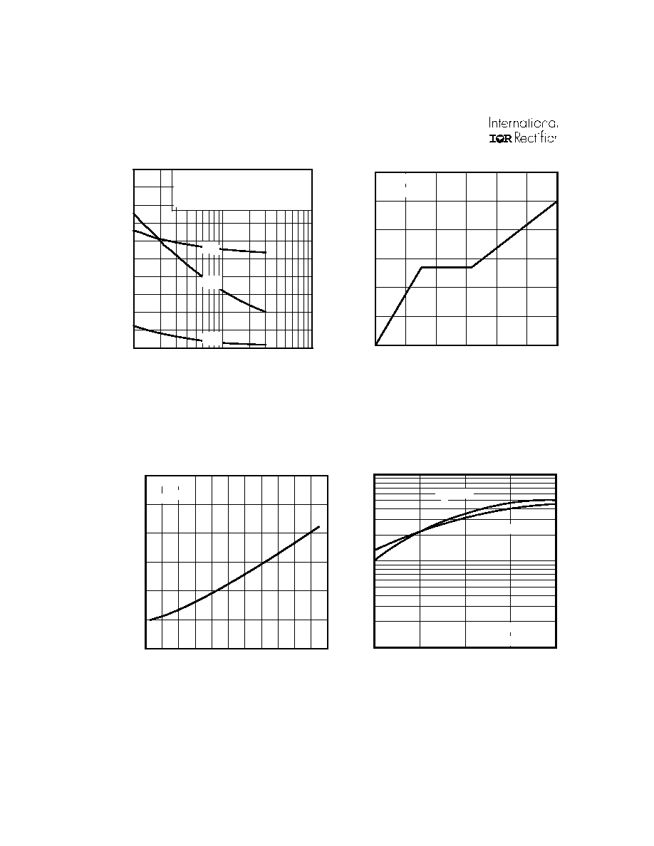
Fig 5. Typical Capacitance Vs.
Drain-to-Source Voltage
Fig 6. Typical Gate Charge Vs.
Gate-to-Source Voltage
Fig 8. Typical Transfer Characteristics
1
10
100
0
400
800
1200
1600
2000
V , Drain-to-Source Voltage (V)
C, Capacitance (pF)
DS
V
C
C
C
=
=
=
=
0V,
C
C
C
f = 1MHz
+ C
+ C
C SHORTED
GS
iss
gs
gd ,
ds
rss
gd
oss
ds
gd
Ciss
Coss
Crss
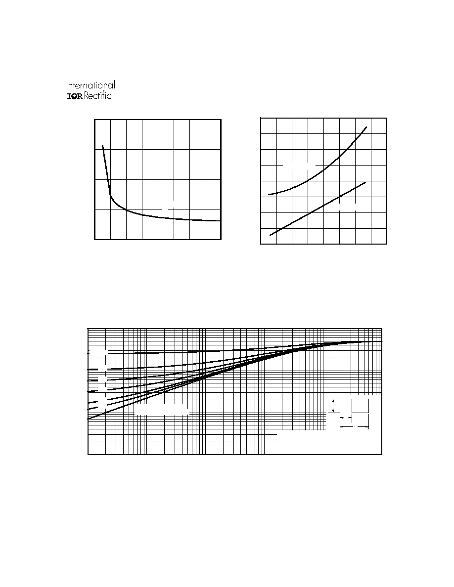
Fig 7. Normalized On-Resistance
Vs. Temperature
0
2
4
6
8
10
12
QG, Total Gate Charge (nC)
0.0
2.0
4.0
6.0
V
GS
, Gate-to-Source Voltage (V)
ID= 7.0A
VDS = 16V
-60 -40 -20
0
20
40
60
80 100 120 140 160
TJ , Junction Temperature ( °C )
0.5
1.0
1.5
2.0
R
DS(on)
, Drain-to-Source On Resistance
(Normalized)
ID = 7.0A
VGS = 4.5V
2.5
3.0
3.5
VGS, Gate-to-Source Voltage (V)
1
10
100
I D
, Drain-to-Source Current
(
A)
TJ = 25°C
TJ = 150°C
VDS = 10V
380µs PULSE WIDTH
IRF7807D1
www.irf.com
5
Fig 11. Maximum Effective Transient Thermal Impedance, Junction-to-Ambient
(
HEXFET
®
MOSFET
)
0.1
1
10
100
0.001
0.01
0.1
1
10
100
Notes:
1. Duty factor D = t / t
2. Peak T = P
x Z
+ T
1
2
J
DM
thJA
A
P
t
t
DM
1
2
t , Rectangular Pulse Duration (sec)
Thermal Response
(Z )
1
thJA
0.01
0.02
0.05
0.10
0.20
D = 0.50
SINGLE PULSE
(THERMAL RESPONSE)
Fig 9. On-Resistance Vs. Gate Voltage
0
20
40
60
80
0.016
0.018
0.020
0.022
0.024
R , Drain-to-Source On Resistance
I , Drain Current (A)
D
DS (on)
VGS = 10V
VGS = 4.5V
Fig 10. On-Resistance Vs. Drain Current
( )
2.0
4.0
6.0
8.0
10.0
VGS, Gate -to -Source Voltage (V)
0.01
0.02
0.03
0.04
0.05
R
DS(on)
, Drain-to -Source On Resistance (
)
ID = 7.0A