 | –≠–ª–µ–∫—Ç—Ä–æ–Ω–Ω—ã–π –∫–æ–º–ø–æ–Ω–µ–Ω—Ç: IRF7807D2 | –°–∫–∞—á–∞—Ç—å:  PDF PDF  ZIP ZIP |
∑ Co-Pack N-channel HEXFET
Æ
Power MOSFET
and Schottky Diode
∑ Ideal for Synchronous Rectifiers in DC-DC
Converters up to 5A Output
∑ Low Conduction Losses
∑ Low Switching Losses
∑ Low Vf Schottky Rectifier
FETKYTM MOSFET / SCHOTTKY DIODE
Parameter
Max.
Units
Maximum Junction-to-Ambient
R
JA
50
∞C/W
Thermal Resistance
Description
The FETKY
TM
family of Co-Pack HEXFET
Æ
MOSFETs
and Schottky diodes offers the designer an innovative,
board space saving solution for switching regulator and
power management applications. HEXFET power
MOSFETs utilize advanced processing techniques to
achieve extremely low on-resistance per silicon area.
Combining this technology with International Rectifier's
low forward drop Schottky rectifiers results in an extremely
efficient device suitable for use in a wide variety of
portable electronics applications.
The SO-8 has been modified through a customized
leadframe for enhanced thermal characteristics. The SO-
8 package is designed for vapor phase, infrared or wave
soldering techniques.
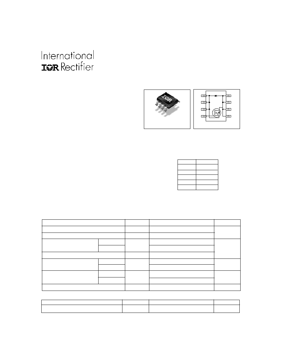
Top View
8
1
2
3
4
5
6
7
A/S
A/S
A/S
G
K/D
K/D
D
K/D
K/D
IRF7807D2
PD- 93762
www.irf.com
1
11/8/99
IRF7807D2
V
DS
30V
R
DS
(on)
25m
Q
g
14nC
Q
SW
5.2nC
Q
oss
21.6nC
Device Features (Max Values)
SO-8
Parameter
Symbol
Max.
Units
Drain-Source Voltage
V
DS
30
Gate-Source Voltage
V
GS
±12
Continuous Drain or Source
25∞C
I
D
8.3
Current (V
GS
4.5V)
70∞C
6.6
A
Pulsed Drain Current
I
DM
66
Power Dissipation
25∞C
P
D
2.5
70∞C
1.6
Schottky and Body Diode
25∞C
I
F
(AV)
3.7
A
Average ForwardCurrent
70∞C
2.3
Junction & Storage Temperature Range
T
J
,
T
STG
≠55 to 150
∞C
Absolute Maximum Ratings
V
W
IRF7807D2
2
www.irf.com
Schottky Diode & Body Diode Ratings and Characteristics
Parameter
Min
Typ
Max
Units
Conditions
Diode Forward Voltage
V
SD
0.54
V
T
j
= 25∞C, I
s
= 3A, V
GS
=0V
0.43
T
j
= 125∞C, I
s
= 3A, V
GS
=0V
Reverse Recovery Time
trr
36
ns
T
j
= 25∞C, I
s
= 7.0A, V
DS
= 16V
Reverse Recovery Charge
Qrr
41
nC
di/dt = 100A/µs
Forward Turn-On Time
t
on
Intrinsic turn-on time is negligible (turn-on is dominated by L
S
+L
D
)
Repetitive rating; pulse width limited by max. junction temperature.
Pulse width
300 µs; duty cycle
2%.
When mounted on 1 inch square copper board, t < 10 sec.
50% Duty Cycle, Rectangular
*
Devices are 100% tested to these parameters.
Electrical Characteristics
Parameter
Min
Typ
Max
Units
Conditions
Drain-to-Source
V
(BR)DSS
30
V
V
GS
= 0V, I
D
= 250µA
Breakdown Voltage*
Static Drain-Source
R
DS
(on)
17
25
m
V
GS
= 4.5V, I
D
= 7A
on Resistance*
Gate Threshold Voltage* V
GS
(th)
1.0
V
V
DS
= V
GS
,I
D
= 250µA
Drain-Source Leakage
I
DSS
90
µ
A
V
DS
= 24V, V
GS
= 0V
Current*
7.2
mA
V
DS
= 24V, V
GS
= 0V,
T
j
= 125∞C
Gate-Source Leakage
I
GSS
+/- 100
nA
V
GS
= +/-12V
Current*
Total Gate Charge
Q
gsync
10.5
14
V
DS
<100mV,
Synch FET*
V
GS
= 5V, I
D
= 7A
Total Gate Charge
Q
gcont
12
17
V
DS
= 16V,
Control FET*
V
GS
= 5V, I
D
= 7A
Pre-Vth
Q
gs1
2.1
V
DS
= 16V, I
D
= 7A
Gate-Source Charge
Post-Vth
Q
gs2
0.76
nC
Gate-Source Charge
Gate to Drain Charge
Q
gd
2.9
Switch Charge*
Q
SW
3.66
5.2
(Q
gs2
+ Q
gd
)
Output Charge*
Q
oss
17.6
21.6
V
DS
= 16V, V
GS
= 0
Gate Resistance
R
g
1.2
IRF7807D2
www.irf.com
3
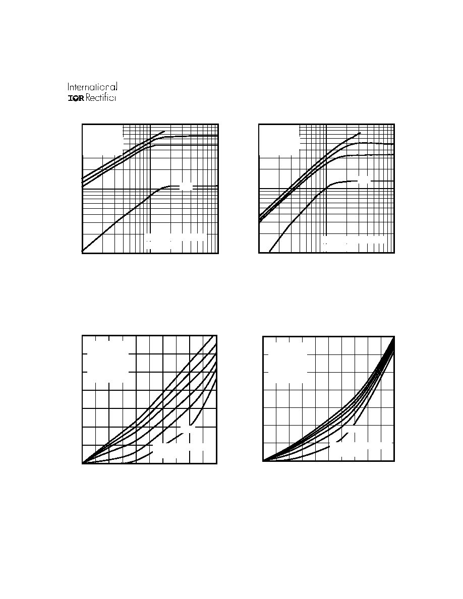
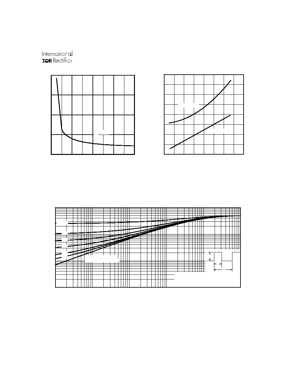
Fig 3. Typical Reverse Output Characteristics
Fig 4. Typical Reverse Output Characteristics
Fig 2. Typical Output Characteristics
Fig 1. Typical Output Characteristics
0.1
1
10
VDS, Drain-to-Source Voltage (V)
1
10
100
I D
, Drain-to-Source Current (A)
380µs PULSE WIDTH
Tj = 25∞C
2.5V
VGS
TOP 4.5V
3.5V
3.0V
BOTTOM 2.5V
0.1
1
10
VDS, Drain-to-Source Voltage (V)
1
10
100
I D
, Drain-to-Source Current (A)
380µs PULSE WIDTH
Tj = 150∞C
VGS
TOP 4.5V
3.5V
3.0V
BOTTOM 2.5V
2.5V
0
0.2
0.4
0.6
0.8
1
VSD, Source-to-Drain Voltage (V)
0
10
20
30
40
50
60
70
I S
, Source-to-Drain Current (A)
380µs PULSE WIDTH
Tj = 25∞C
VGS
TOP 4.5V
3.5V
3.0V
2.5V
2.0V
BOTTOM 0.0V
0.0 V
0
0.2
0.4
0.6
0.8
1
VSD, Source-to-Drain Voltage (V)
0
10
20
30
40
50
60
70
I S
, Source-to-Drain Current (A)
380µS PULSE WIDTH
Tj = 150∞C
VGS
TOP 4.5V
3.5V
3.0V
2.5V
2.0V
BOTTOM 0.0V
O.OV
IRF7807D2
4
www.irf.com
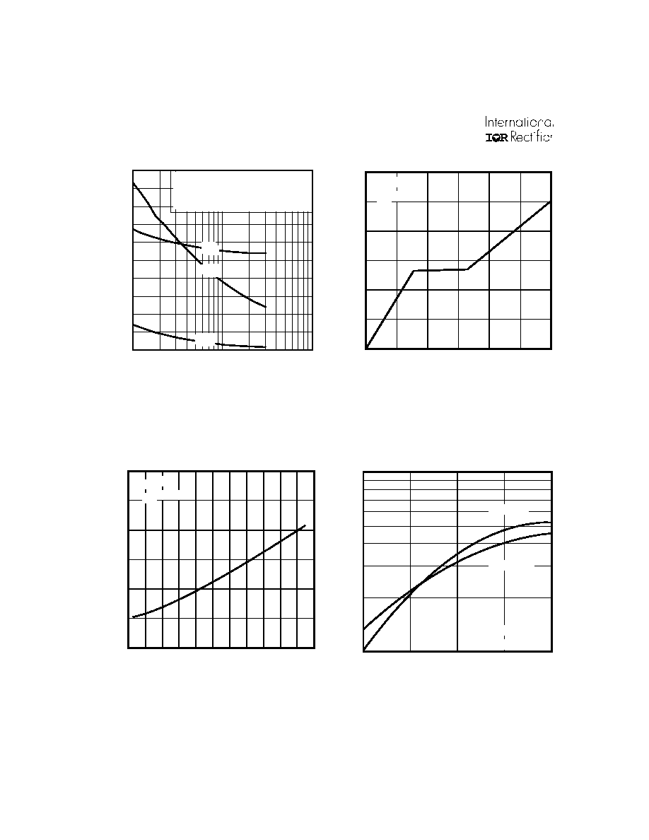
Fig 5. Typical Capacitance Vs.
Drain-to-Source Voltage
Fig 6. Typical Gate Charge Vs.
Gate-to-Source Voltage
Fig 8. Typical Transfer Characteristics
Fig 7. Normalized On-Resistance
Vs. Temperature
1
10
100
0
400
800
1200
1600
2000
V , Drain-to-Source Voltage (V)
C, Capacitance (pF)
DS
V
C
C
C
=
=
=
=
0V,
C
C
C
f = 1MHz
+ C
+ C
C SHORTED
GS
iss
gs
gd ,
ds
rss
gd
oss
ds
gd
C
rss
C
oss
C
iss
0
4
8
12
QG, Total Gate Charge (nC)
0
2
4
6
V
GS
, Gate-to-Source Voltage (V)
ID= 7.0A
VDS = 16V
-60 -40 -20
0
20
40
60
80 100 120 140 160
TJ, Junction Temperature (∞C )
0.5
1.0
1.5
2.0
R
DS(on)
, Drain-to-Source On Resistance
(Normalized)
ID = 7.0A
VGS = 4.5V
2.5
3.0
3.5
VGS, Gate-to-Source Voltage (V)
10
100
I D
, Drain-to-Source Current
(
)
TJ = 25∞C
TJ = 150∞C
VDS = 10V
380µs PULSE WIDTH
IRF7807D2
www.irf.com
5
Fig 11. Maximum Effective Transient Thermal Impedance, Junction-to-Ambient (MOSFET)
0.1
1
10
100
0.001
0.01
0.1
1
10
100
Notes:
1. Duty factor D = t / t
2. Peak T = P
x Z
+ T
1
2
J
DM
thJA
A
P
t
t
DM
1
2
t , Rectangular Pulse Duration (sec)
Thermal Response
(Z )
1
thJA
0.01
0.02
0.05
0.10
0.20
D = 0.50
SINGLE PULSE
(THERMAL RESPONSE)
Fig 9. On-Resistance Vs. Gate Voltage
0
20
40
60
80
0.016
0.018
0.020
0.022
0.024
R , Drain-to-Source On Resistance
I , Drain Current (A)
D
DS (on)
VGS = 10V
VGS = 4.5V
Fig 10. On-Resistance Vs. Drain Current
( )
2.0
4.0
6.0
8.0
10.0
VGS, Gate -to -Source Voltage (V)
0.01
0.02
0.03
0.04
0.05
R
DS(on)
, Drain-to -Source On Resistance (
)
ID = 7.0A
IRF7807D2
6
www.irf.com
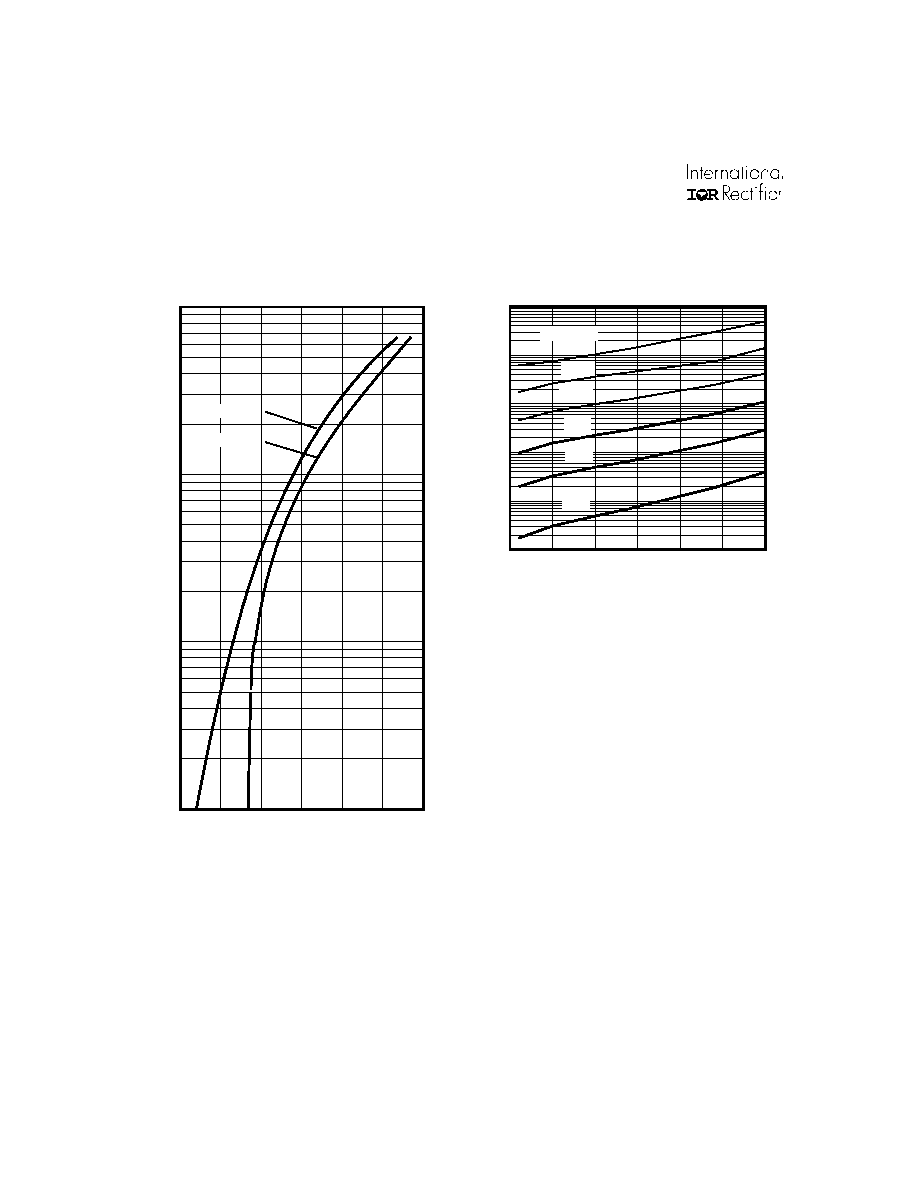
Mosfet, Body Diode & Schottky Diode Characteristics
Fig. 13 - Typical Values of
Reverse Current Vs. Reverse Voltage
Fig. 12 - Typical Forward Voltage Drop
Characteristics
0.0
0.2
0.4
0.6
0.8
1.0
1.2
Forward Voltage Drop - V SD ( V )
0.1
1
10
100
Instantaneous Forward Current - I
F
( A )
Tj = 125∞C
Tj = 25∞C
0
5
10
15
20
25
30
Reverse Voltage - VR (V)
0.001
0.01
0.1
1
10
100
Reverse Current - I
R
( mA )
125∞C
100∞C
Tj = 150∞C
75∞C
50∞C
25∞C
IRF7807D2
www.irf.com
7
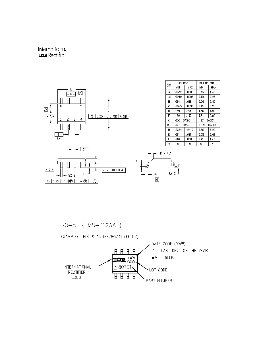
SO-8 Package Details
Part Marking
IRF7807D2
8
www.irf.com
33 0.00
(12 .9 92 )
M A X .
14 .4 0 ( .5 66 )
12 .4 0 ( .4 88 )
N O T E S :
1. C O N T R O LL IN G D IM E N S IO N : M IL L IM E T E R .
2. O U T L IN E C O N F O R M S T O E IA -48 1 & E IA -54 1.
F E E D D IR E C T IO N
T E R M IN A L N U M B E R 1
12 .3 ( .48 4 )
11 .7 ( .46 1 )
8 .1 ( .31 8 )
7 .9 ( .31 2 )
N O T E S :
1 . C O N T R O L L IN G D IM E N S IO N : M IL L IM E T E R .
2 . A L L D IM E N S IO N S A R E S H O W N IN M IL L IM E TE R S (IN C H E S ).
3 . O U T L IN E C O N F O R M S T O E IA -4 8 1 & E IA -5 4 1.
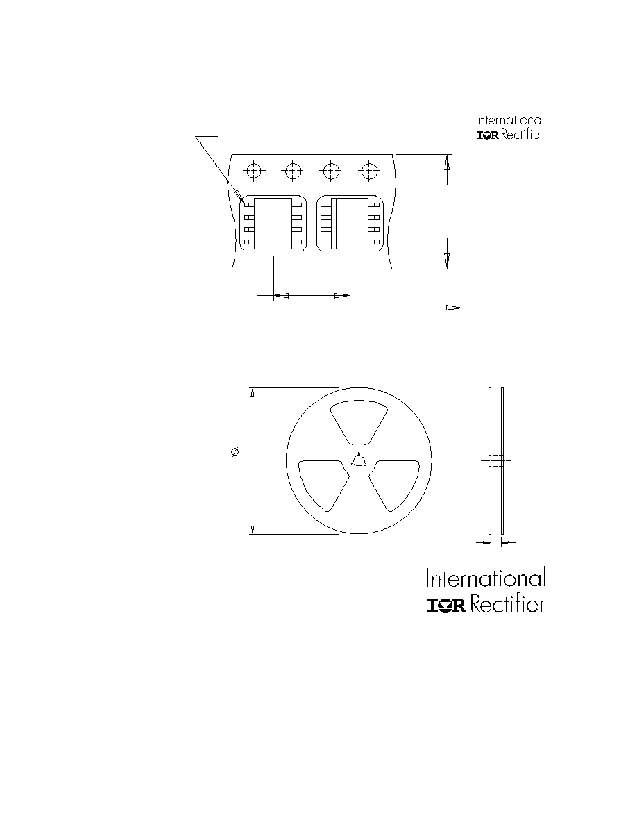
Tape and Reel
WORLD HEADQUARTERS: 233 Kansas St., El Segundo, California 90245, Tel: (310) 322 3331
IR GREAT BRITAIN: Hurst Green, Oxted, Surrey RH8 9BB, UK Tel: ++ 44 1883 732020
IR CANADA: 15 Lincoln Court, Brampton, Ontario L6T3Z2, Tel: (905) 453 2200
IR GERMANY: Saalburgstrasse 157, 61350 Bad Homburg Tel: ++ 49 6172 96590
IR ITALY: Via Liguria 49, 10071 Borgaro, Torino Tel: ++ 39 11 451 0111
IR JAPAN: K&H Bldg., 2F, 30-4 Nishi-Ikebukuro 3-Chome, Toshima-Ku, Tokyo Japan 171 Tel: 81 3 3983 0086
IR SOUTHEAST ASIA: 1 Kim Seng Promenade, Great World City West Tower, 13-11, Singapore 237994 Tel: ++ 65 838 4630
IR TAIWAN:16 Fl. Suite D. 207, Sec. 2, Tun Haw South Road, Taipei, 10673, Taiwan Tel: 886-2-2377-9936
Data and specifications subject to change without notice. 11/99