 | ÐлекÑÑоннÑй компоненÑ: IRF7809AV | СкаÑаÑÑ:  PDF PDF  ZIP ZIP |
Äîêóìåíòàöèÿ è îïèñàíèÿ www.docs.chipfind.ru
Parameter
Symbol
IRF7809A V
Units
Drain-Source Voltage
V
DS
30
V
Gate-Source Voltage
V
GS
±12
Continuous Drain or Source
T
A
= 25°C
I
D
13.3
Current (V
GS
4.5V)
T
L
= 90°C
14.6
A
Pulsed Drain Current
I
DM
100
Power Dissipation
T
A
= 25°C
P
D
2.5
W
T
L
= 90°C
3.0
Junction & Storage Temperature Range
T
J
,
T
STG
55 to 150
°C
Continuous Source Current (Body Diode)
I
S
2.5
A
Pulsed Source Current
I
SM
50
· N-Channel Application-Specific MOSFETs
· Ideal for CPU Core DC-DC Converters
· Low Conduction Losses
· Low Switching Losses
· Minimizes Parallel MOSFETs for high current
applications
Description
This new device employs advanced HEXFET Power
MOSFET technology to achieve an unprecedented
balance of on-resistance and gate charge. The reduced
conduction and switching losses make it ideal for high
efficiency DC-DC converters that power the latest
generation of microprocessors.
The IRF7809AV has been optimized for all parameters
that are critical in synchronous buck converters including
R
DS(on)
, gate charge and Cdv/dt-induced turn-on immunity.
The IRF7809AV offers particulary low R
DS(on)
and high
Cdv/dt immunity for synchronous FET applications.
The package is designed for vapor phase, infra-red,
convection, or wave soldering techniques. Power
dissipation of greater than 2W is possible in a typical
PCB mount application.
Absolute Maximum Ratings
Parameter
Max.
Units
Maximum Junction-to-Ambient
R
JA
50
°C/W
Maximum Junction-to-Lead
R
JL
20
°C/W
Thermal Resistance
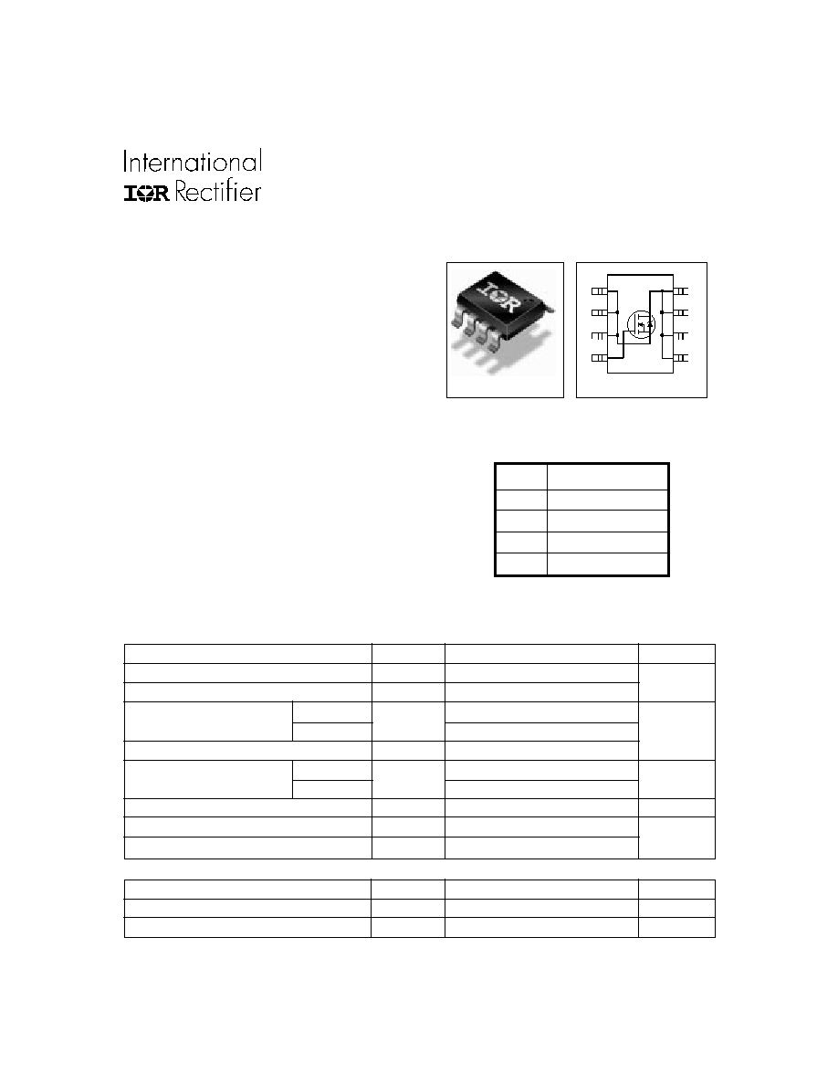
T o p V ie w
8
1
2
3
4
5
6
7
D
D
D
D
G
S
A
S
S
A
PD-90010
IRF7809AV
SO-8
10/26/00
IRF7809AV
R
DS
(on)
7.0m
Q
G
41nC
Q
sw
14nC
Q
oss
30nC
DEVICE CHARACTERISTICS
IRF7809AV
2
www.irf.com
Parameter
Min
Typ
Max
Units
Conditions
Diode Forward
V
SD
1.3
V
I
S
= 15A
, V
GS
= 0V
Voltage*
Reverse Recovery
Q
rr
120
nC
di/dt
~
700A/µs
V
DS
= 16V, V
GS
= 0V, I
S
= 15A
Reverse Recovery
Q
rr(s)
150
nC
di/dt = 700A/µs
Charge (with Parallel
(with 10BQ040)
Schottky)
V
DS
= 16V, V
GS
= 0V, I
S
= 15A
Parameter
Min
Typ
Max
Units
Conditions
Drain-to-Source
BV
DSS
30
V
V
GS
= 0V, I
D
= 250µA
Breakdown Voltage
Static Drain-Source
R
DS(on)
7.0
9.0
m
V
GS
= 4.5V, I
D
= 15A
on Resistance
Gate Threshold Voltage
V
GS(th)
1.0
V
V
DS
= V
GS
,I
D
= 250µA
Drain-Source Leakage
I
DSS
30
V
DS
= 24V, V
GS
= 0
Current*
150
µA
V
DS
= 24V, V
GS
= 0,
Tj = 100°C
Gate-Source Leakage
I
GSS
±100
nA
V
GS
= ±12V
Current*
Total Gate Chg Cont FET
Q
G
41
62
V
GS
=5V, I
D
=15A, V
DS
=20V
Total Gate Chg Sync FET
Q
G
36
54
V
GS
= 5V, V
DS
< 100mV
Pre-Vth
Q
GS1
7.0
V
DS
= 20V, I
D
= 15A
Gate-Source Charge
Post-Vth
Q
GS2
2.3
nC
Gate-Source Charge
Gate to Drain Charge
Q
GD
12
I
D
=15A, V
DS
=16V
Switch Chg(Q
gs2
+ Q
gd
)
Q
sw
14
21
Output Charge*
Q
oss
30
45
V
DS
= 16V, V
GS
= 0
Gate Resistance
R
G
1.5
Turn-on Delay Time
t
d (on)
14
V
DD
= 16V, I
D
= 15A
Rise Time
t
r
36
ns
V
GS
= 5V
Turn-off Delay Time
t
d
(off)
96
Clamped Inductive Load
Fall Time
t
f
10
Input Capacitance
C
iss
3780
Output Capacitance
C
oss
1060
pF
V
DS
= 16V, V
GS
= 0
Reverse Transfer Capacitance C
rss
130
Electrical Characteristics
Source-Drain Rating & Characteristics
Current
Charge
Notes:
Repetitive rating; pulse width limited by max. junction temperature.
Pulse width
400 µs; duty cycle
2%.
When mounted on 1 inch square copper board, t < 10 sec.
Typ = measured - Q
oss
Typical values measured at V
GS
= 4.5V, I
F
= 15A.
IRF7809AV
www.irf.com
3
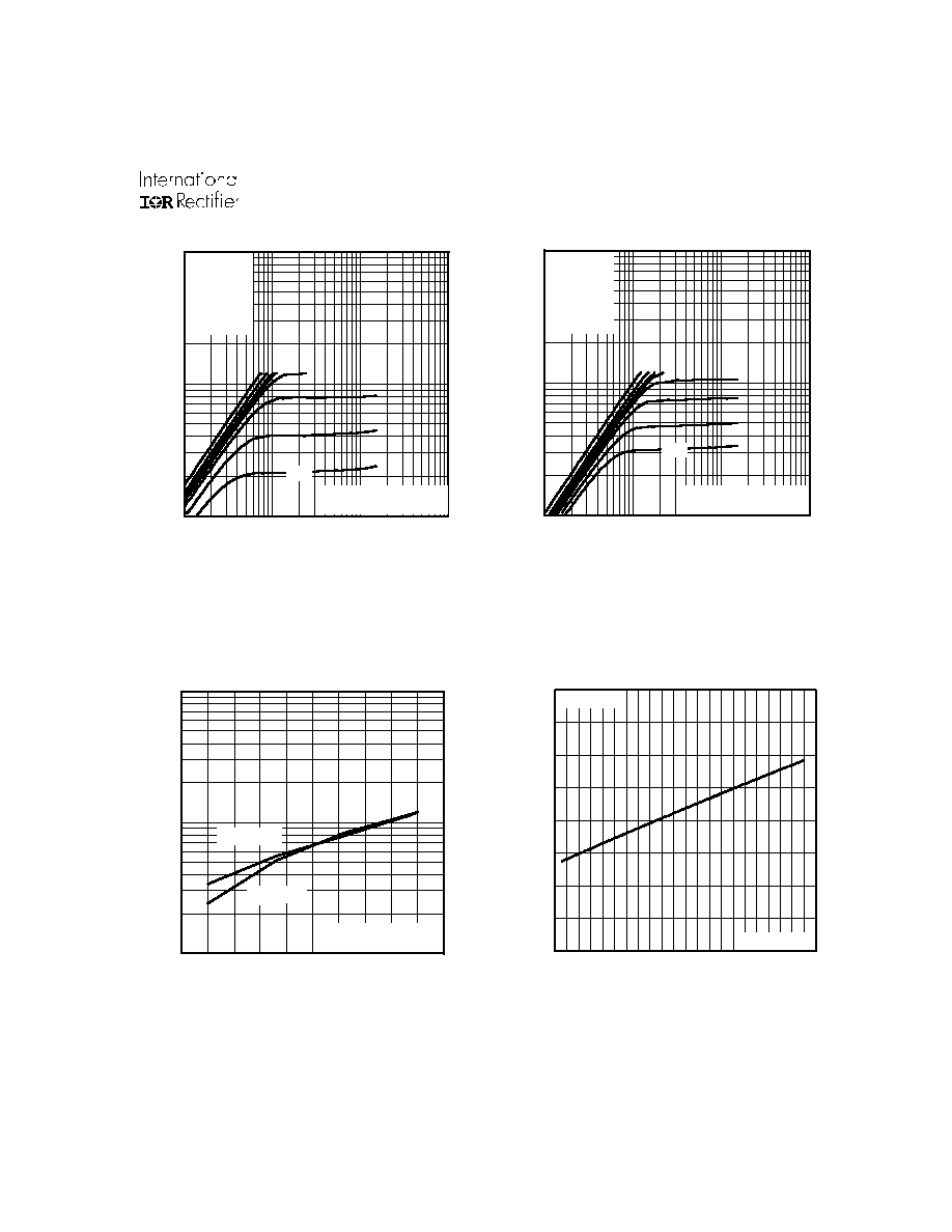
Fig 2. Typical Output Characteristics
Fig 1. Typical Output Characteristics
Fig 3. Typical Transfer Characteristics
Fig 4. Normalized On-Resistance
Vs. Temperature
10
100
1000
0.1
1
10
100
20µs PULSE WIDTH
T = 25 C
J
°
TOP
BOTTOM
VGS
10V
4.5V
3.7V
3.5V
3.3V
3.0V
2.7V
2.5V
V , Drain-to-Source Voltage (V)
I , Drain-to-Source Current (A)
DS
D
2.5V
10
100
1000
0.1
1
10
100
20µs PULSE WIDTH
T = 150 C
J
°
TOP
BOTTOM
VGS
10V
4.5V
3.7V
3.5V
3.3V
3.0V
2.7V
2.5V
V , Drain-to-Source Voltage (V)
I , Drain-to-Source Current (A)
DS
D
2.5V
10
100
1000
2.4
2.6
2.8
3.0
3.2
3.4
V = 15V
20µs PULSE WIDTH
DS
V , Gate-to-Source Voltage (V)
I , Drain-to-Source Current (A)
GS
D
T = 25 C
J
°
T = 150 C
J
°
-60 -40 -20
0
20
40
60
80 100 120 140 160
0.0
0.5
1.0
1.5
2.0
T , Junction Temperature ( C)
R , Drain-to-Source On Resistance
(Normalized)
J
DS(on)
°
V
=
I =
GS
D
10V
15A
IRF7809AV
4
www.irf.com
Fig 6. Typical Gate Charge Vs.
Gate-to-Source Voltage
Fig 5. Typical Capacitance Vs.
Drain-to-Source Voltage
Fig 7. Typical Source-Drain Diode
Forward Voltage
Fig 8. Maximum Safe Operating Area
1
10
100
0
1000
2000
3000
4000
5000
6000
V , Drain-to-Source Voltage (V)
C, Capacitance (pF)
DS
V
C
C
C
=
=
=
=
0V,
C
C
C
f = 1MHz
+ C
+ C
C SHORTED
GS
iss
gs
gd ,
ds
rss
gd
oss
ds
gd
C
iss
C
oss
C
rss
0.1
1
10
100
1000
0.2
0.6
1.0
1.4
1.8
2.2
V ,Source-to-Drain Voltage (V)
I , Reverse Drain Current (A)
SD
SD
V = 0 V
GS
T = 25 C
J
°
T = 150 C
J
°
1
10
100
1000
0.1
1
10
100
OPERATION IN THIS AREA LIMITED
BY R
DS(on)
Single Pulse
T
T
= 150 C
= 25 C
°
°
J
A
V , Drain-to-Source Voltage (V)
I , Drain Current (A)
I , Drain Current (A)
DS
D
10us
100us
1ms
10ms
0
10
20
30
40
50
60
70
0
2
4
6
8
10
Q , Total Gate Charge (nC)
V , Gate-to-Source Voltage (V)
G
GS
I =
D
15A
V
= 20V
DS
IRF7809AV
www.irf.com
5
Fig 11. Maximum Effective Transient Thermal Impedance, Junction-to-Ambient
Fig 9. Maximum Drain Current Vs.
Case Temperature
Fig 10a. Switching Time Test Circuit
V
DS
90%
10%
V
GS
t
d(on)
t
r
t
d(off)
t
f
Fig 10b. Switching Time Waveforms
V
DS
Pulse Width
1
µs
Duty Factor
0.1 %
R
D
V
GS
R
G
D.U.T.
10V
+
-
V
DD
25
50
75
100
125
150
0
4
8
12
16
T , Case Temperature
( C)
I , Drain Current (A)
°
C
D
0.01
0.1
1
10
100
0.00001
0.0001
0.001
0.01
0.1
1
10
100
Notes:
1. Duty factor D = t / t
2. Peak T = P
x Z
+ T
1
2
J
DM
thJA
A
P
t
t
DM
1
2
t , Rectangular Pulse Duration (sec)
Thermal Response
(Z )
1
thJA
0.01
0.02
0.05
0.10
0.20
D = 0.50
SINGLE PULSE
(THERMAL RESPONSE)