 | –≠–ª–µ–∫—Ç—Ä–æ–Ω–Ω—ã–π –∫–æ–º–ø–æ–Ω–µ–Ω—Ç: IRF8910 | –°–∫–∞—á–∞—Ç—å:  PDF PDF  ZIP ZIP |
www.irf.com
1
4/28/04
IRF8910
HEXFET
Æ
Power MOSFET
Notes
through
are on page 10
SO-8
PD - 95868
Benefits
l
Very Low R
DS(on)
at 4.5V V
GS
l
Ultra-Low Gate Impedance
l
Fully Characterized Avalanche Voltage
and Current
l
20V V
GS
Max. Gate Rating
Absolute Maximum Ratings
Parameter
Units
V
DS
Drain-to-Source Voltage
V
V
GS
Gate-to-Source Voltage
I
D
@ T
A
= 25∞C
Continuous Drain Current, V
GS
@ 10V
I
D
@ T
A
= 70∞C
Continuous Drain Current, V
GS
@ 10V
A
I
DM
Pulsed Drain Current
c
P
D
@T
A
= 25∞C
Power Dissipation
W
P
D
@T
A
= 70∞C
Power Dissipation
Linear Derating Factor
W/∞C
T
J
Operating Junction and
∞C
T
STG
Storage Temperature Range
Thermal Resistance
Parameter
Typ.
Max.
Units
R
JL
Junction-to-Drain Lead
≠≠≠
20
∞C/W
R
JA
Junction-to-Ambient
fg
≠≠≠
62.5
Max.
10
8.3
82
± 20
20
-55 to + 150
2.0
0.016
1.3
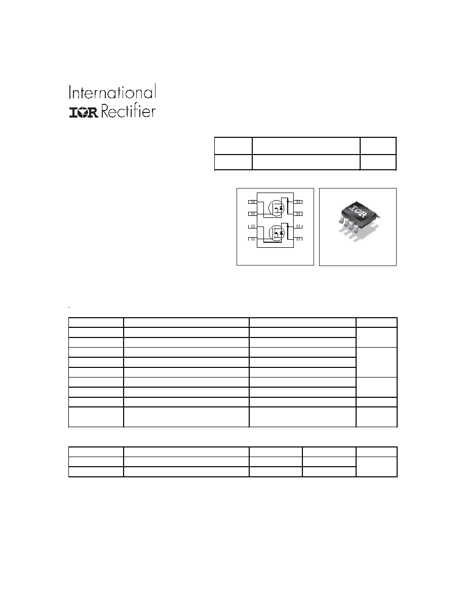
D1
D1
D2
D2
G1
S2
G2
S1
Top View
8
1
2
3
4
5
6
7
Applications
l
Dual SO-8 MOSFET for POL
converters in desktop, servers,
graphics cards, game consoles
and set-top box
V
DSS
R
DS(on)
max
I
D
20V
13.4m:@V
GS
= 10V
10A
IRF8910
2
www.irf.com
S
D
G
Static @ T
J
= 25∞C (unless otherwise specified)
Parameter
Min. Typ. Max. Units
BV
DSS
Drain-to-Source Breakdown Voltage
20
≠≠≠
≠≠≠
V
V
DSS
/
T
J
Breakdown Voltage Temp. Coefficient
≠≠≠
0.015
≠≠≠
V/∞C
R
DS(on)
Static Drain-to-Source On-Resistance
≠≠≠
10.7
13.4
m
≠≠≠
14.6
18.3
V
GS(th)
Gate Threshold Voltage
1.65
≠≠≠
2.55
V
V
GS(th)
/
T
J
Gate Threshold Voltage Coefficient
≠≠≠
-4.8
≠≠≠
mV/∞C
I
DSS
Drain-to-Source Leakage Current
≠≠≠
≠≠≠
1.0
µA
≠≠≠
≠≠≠
150
I
GSS
Gate-to-Source Forward Leakage
≠≠≠
≠≠≠
100
nA
Gate-to-Source Reverse Leakage
≠≠≠
≠≠≠
-100
gfs
Forward Transconductance
24
≠≠≠
≠≠≠
S
Q
g
Total Gate Charge
≠≠≠
7.4
11
Q
gs1
Pre-Vth Gate-to-Source Charge
≠≠≠
2.4
≠≠≠
Q
gs2
Post-Vth Gate-to-Source Charge
≠≠≠
0.80
≠≠≠
nC
Q
gd
Gate-to-Drain Charge
≠≠≠
2.5
≠≠≠
Q
godr
Gate Charge Overdrive
≠≠≠
1.7
≠≠≠
See Fig. 6
Q
sw
Switch Charge (Q
gs2
+ Q
gd
)
≠≠≠
3.3
≠≠≠
Q
oss
Output Charge
≠≠≠
4.4
≠≠≠
nC
t
d(on)
Turn-On Delay Time
≠≠≠
6.2
≠≠≠
t
r
Rise Time
≠≠≠
10
≠≠≠
ns
t
d(off)
Turn-Off Delay Time
≠≠≠
9.7
≠≠≠
t
f
Fall Time
≠≠≠
4.1
≠≠≠
C
iss
Input Capacitance
≠≠≠
960
≠≠≠
C
oss
Output Capacitance
≠≠≠
300
≠≠≠
pF
C
rss
Reverse Transfer Capacitance
≠≠≠
160
≠≠≠
Avalanche Characteristics
Parameter
Units
E
AS
Single Pulse Avalanche Energy
d
mJ
I
AR
Avalanche Current
A
Diode Characteristics
Parameter
Min. Typ. Max. Units
I
S
Continuous Source Current
≠≠≠
≠≠≠
2.5
(Body Diode)
A
I
SM
Pulsed Source Current
≠≠≠
≠≠≠
82
(Body Diode)
√
V
SD
Diode Forward Voltage
≠≠≠
≠≠≠
1.0
V
t
rr
Reverse Recovery Time
≠≠≠
17
26
ns
Q
rr
Reverse Recovery Charge
≠≠≠
6.5
9.7
nC
≠≠≠
I
D
= 8.2A
V
GS
= 0V
V
DS
= 10V
V
GS
= 4.5V, I
D
= 8.0A
e
V
GS
= 4.5V
Typ.
≠≠≠
V
DS
= V
GS
, I
D
= 250µA
Clamped Inductive Load
V
DS
= 10V, I
D
= 8.2A
V
DS
= 16V, V
GS
= 0V, T
J
= 125∞C
T
J
= 25∞C, I
F
= 8.2A, V
DD
= 10V
di/dt = 100A/µs
e
T
J
= 25∞C, I
S
= 8.2A, V
GS
= 0V
e
showing the
integral reverse
p-n junction diode.
MOSFET symbol
V
DS
= 10V, V
GS
= 0V
V
DD
= 10V, V
GS
= 4.5V
I
D
= 8.2A
V
DS
= 10V
V
GS
= 20V
V
GS
= -20V
V
DS
= 16V, V
GS
= 0V
Conditions
V
GS
= 0V, I
D
= 250µA
Reference to 25∞C, I
D
= 1mA
V
GS
= 10V, I
D
= 10A
e
Conditions
Max.
19
8.2
= 1.0MHz
IRF8910
www.irf.com
3
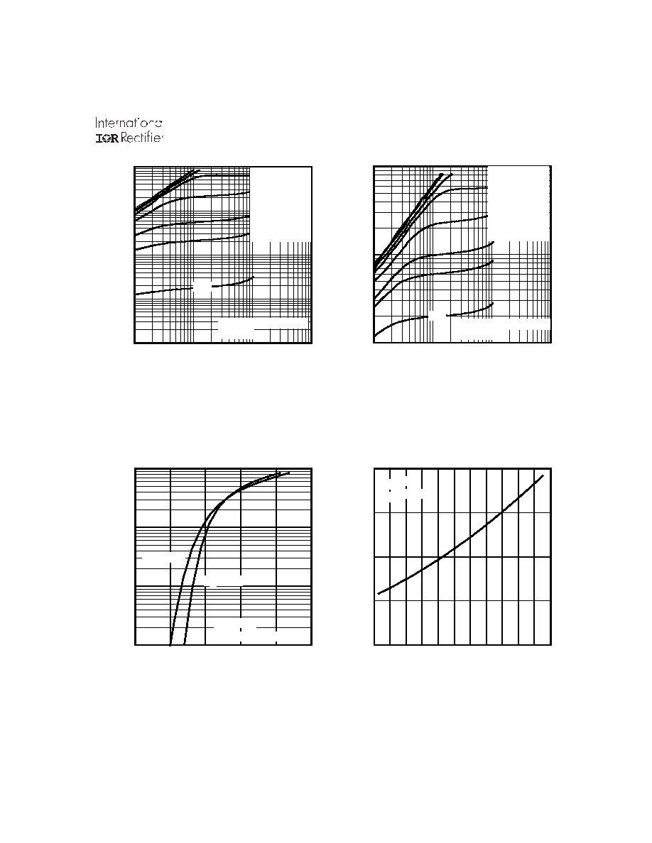
Fig 4. Normalized On-Resistance
vs. Temperature
Fig 2. Typical Output Characteristics
Fig 1. Typical Output Characteristics
Fig 3. Typical Transfer Characteristics
0.1
1
10
100
VDS, Drain-to-Source Voltage (V)
0.01
0.1
1
10
100
I D
,
D
r
a
i
n
-
t
o
-
S
o
u
r
c
e
C
u
r
r
e
n
t
(
A
)
VGS
TOP
10V
8.0V
5.5V
4.5V
3.5V
3.0V
2.8V
BOTTOM
2.5V
60µs PULSE WIDTH
Tj = 25∞C
2.5V
0.1
1
10
100
VDS, Drain-to-Source Voltage (V)
1
10
100
I D
,
D
r
a
i
n
-
t
o
-
S
o
u
r
c
e
C
u
r
r
e
n
t
(
A
)
2.5V
60µs PULSE WIDTH
Tj = 150∞C
VGS
TOP
10V
8.0V
5.5V
4.5V
3.5V
3.0V
2.8V
BOTTOM
2.5V
1
2
3
4
5
6
VGS, Gate-to-Source Voltage (V)
0.1
1
10
100
I D
,
D
r
a
i
n
-
t
o
-
S
o
u
r
c
e
C
u
r
r
e
n
t
(
)
TJ = 25∞C
TJ = 150∞C
VDS = 10V
60µs PULSE WIDTH
-60 -40 -20
0
20 40 60 80 100 120 140 160
TJ , Junction Temperature (∞C)
0.5
1.0
1.5
R
D
S
(
o
n
)
,
D
r
a
i
n
-
t
o
-
S
o
u
r
c
e
O
n
R
e
s
i
s
t
a
n
c
e
(
N
o
r
m
a
l
i
z
e
d
)
ID = 10A
VGS = 10V
IRF8910
4
www.irf.com
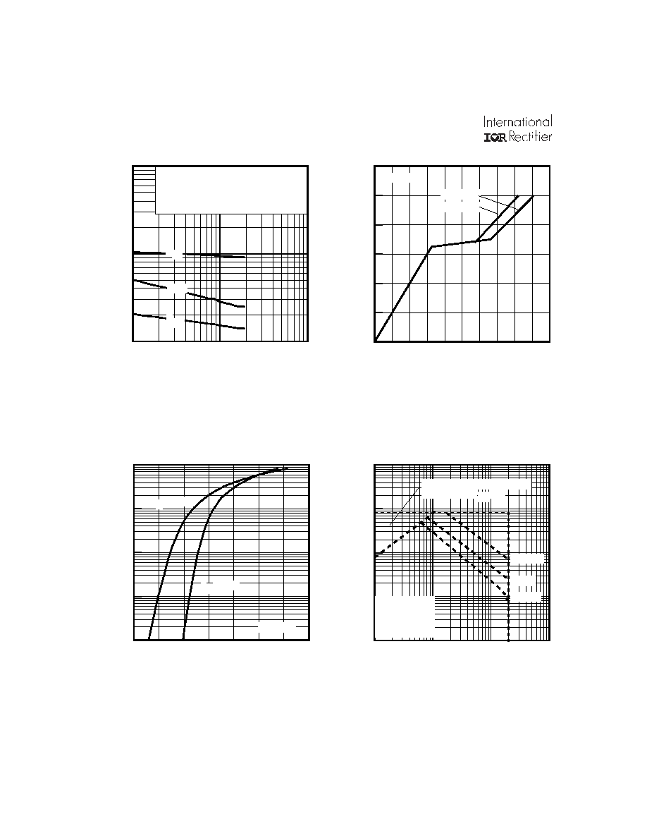
Fig 8. Maximum Safe Operating Area
Fig 6. Typical Gate Charge Vs.
Gate-to-Source Voltage
Fig 5. Typical Capacitance vs.
Drain-to-Source Voltage
Fig 7. Typical Source-Drain Diode
Forward Voltage
1
10
100
VDS, Drain-to-Source Voltage (V)
100
1000
10000
C
,
C
a
p
a
c
i
t
a
n
c
e
(
p
F
)
VGS = 0V, f = 1 MHZ
Ciss = Cgs + Cgd, C ds SHORTED
Crss = Cgd
Coss = Cds + Cgd
Coss
Crss
Ciss
0
1
2
3
4
5
6
7
8
9
10
QG Total Gate Charge (nC)
0.0
1.0
2.0
3.0
4.0
5.0
6.0
V
G
S
,
G
a
t
e
-
t
o
-
S
o
u
r
c
e
V
o
l
t
a
g
e
(
V
)
VDS= 16V
VDS= 10V
ID= 8.2A
0.2
0.4
0.6
0.8
1.0
1.2
1.4
1.6
VSD, Source-to-Drain Voltage (V)
0.01
0.10
1.00
10.00
100.00
I S
D
,
R
e
v
e
r
s
e
D
r
a
i
n
C
u
r
r
e
n
t
(
A
)
TJ = 25∞C
TJ = 150∞C
VGS = 0V
0
1
10
100
VDS, Drain-to-Source Voltage (V)
0.1
1
10
100
1000
I D
,
D
r
a
i
n
-
t
o
-
S
o
u
r
c
e
C
u
r
r
e
n
t
(
A
)
1msec
10msec
OPERATION IN THIS AREA
LIMITED BY RDS(on)
100µsec
TA = 25∞C
Tj = 150∞C
Single Pulse
IRF8910
www.irf.com
5
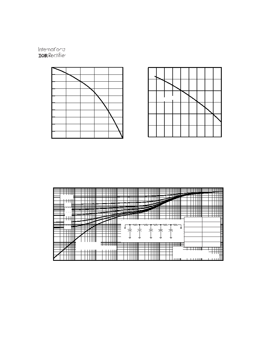
Fig 11. Maximum Effective Transient Thermal Impedance, Junction-to-Ambient
Fig 9. Maximum Drain Current vs.
Ambient Temperature
Fig 10. Threshold Voltage vs. Temperature
25
50
75
100
125
150
TA , Ambient Temperature (∞C)
0
1
2
3
4
5
6
7
8
9
10
I D
,
D
r
a
i
n
C
u
r
r
e
n
t
(
A
)
1E-006
1E-005
0.0001
0.001
0.01
0.1
1
10
100
t1 , Rectangular Pulse Duration (sec)
0.01
0.1
1
10
100
T
h
e
r
m
a
l
R
e
s
p
o
n
s
e
(
Z
t
h
J
A
)
0.20
0.10
D = 0.50
0.02
0.01
0.05
SINGLE PULSE
( THERMAL RESPONSE )
Notes:
1. Duty Factor D = t1/t2
2. Peak Tj = P dm x Zthja + Tc
J
J
1
1
2
2
3
3
R
1
R
1
R
2
R
2
R
3
R
3
Ci=
i/Ri
Ci=
i/Ri
4
4
R
4
R
4
C
C
5
5
R
5
R
5
Ri (∞C/W)
i (sec)
1.2647 0.000091
2.0415 0.000776
18.970 0.188739
23.415 0.757700
16.803 25.10000
-75
-50
-25
0
25
50
75
100 125 150
TJ , Temperature ( ∞C )
1.0
1.5
2.0
2.5
V
G
S
(
t
h
)
G
a
t
e
t
h
r
e
s
h
o
l
d
V
o
l
t
a
g
e
(
V
)
ID = 250µA