 | ÐлекÑÑоннÑй компоненÑ: IRFP064V | СкаÑаÑÑ:  PDF PDF  ZIP ZIP |
Äîêóìåíòàöèÿ è îïèñàíèÿ www.docs.chipfind.ru
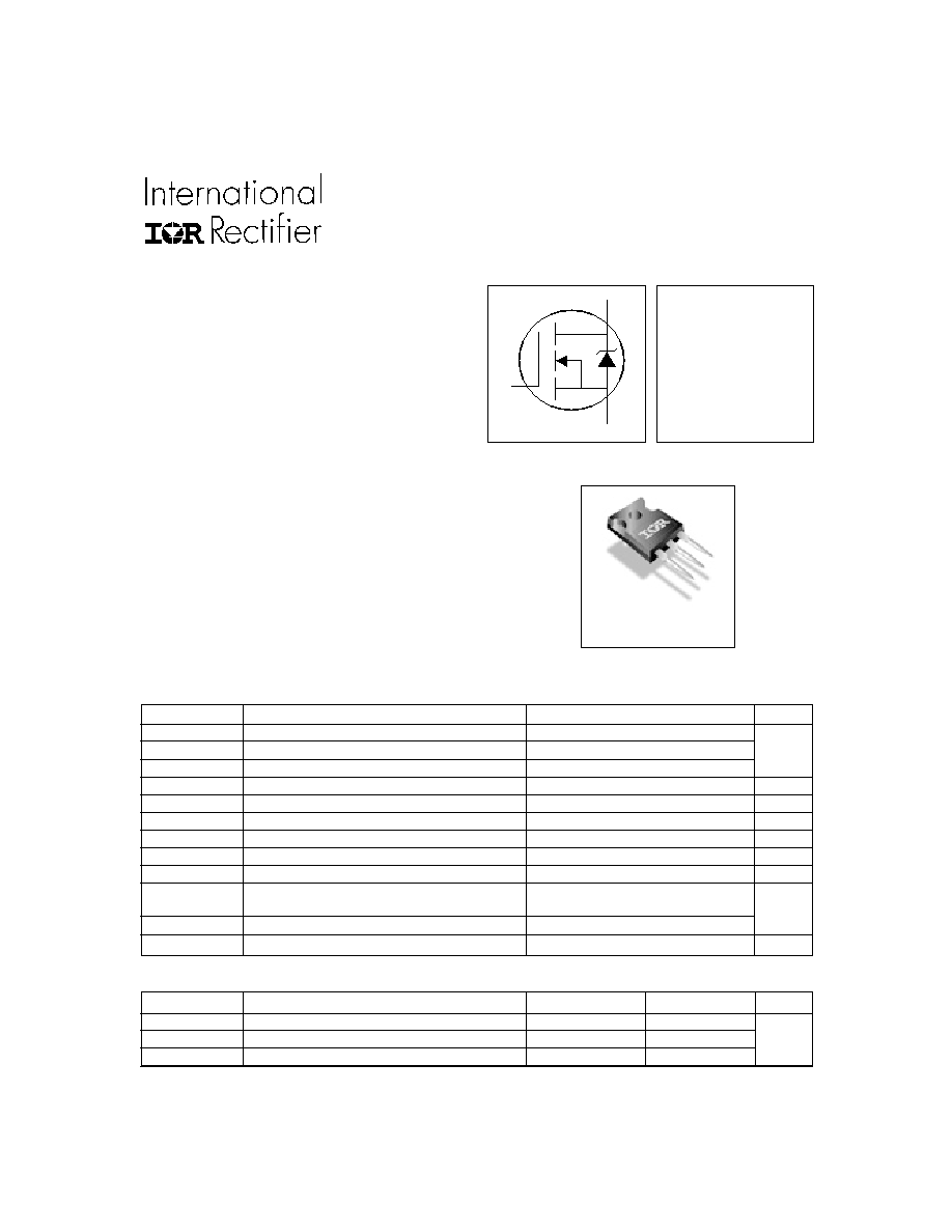
IRFP064V
HEXFET
®
Power MOSFET
3/30/01
Parameter
Typ.
Max.
Units
R
JC
Junction-to-Case
0.60
R
CS
Case-to-Sink, Flat, Greased Surface
0.24
°C/W
R
JA
Junction-to-Ambient
40
Thermal Resistance
www.irf.com
1
V
DSS
= 60V
R
DS(on)
= 5.5m
I
D
= 130A
S
D
G
Advanced HEXFET
®
Power MOSFETs from International
Rectifier utilize advanced processing techniques to achieve
extremely low on-resistance per silicon area. This benefit,
combined with the fast switching speed and ruggedized
device design that HEXFET power MOSFETs are well
known for, provides the designer with an extremely efficient
and reliable device for use in a wide variety of applications.
The TO-247 package is preferred for commercial-industrial
applications where higher power levels preclude the use
of TO-220 devices. The TO-247 is similar but superior to
the earlier TO-218 package because of its isolated
mounting hole.
l
Advanced Process Technology
l
Ultra Low On-Resistance
l
Dynamic dv/dt Rating
l
175°C Operating Temperature
l
Fast Switching
l
Fully Avalanche Rated
l
Optimized for SMPS Applications
Description
PD - 94112
Absolute Maximum Ratings
Parameter
Max.
Units
I
D
@ T
C
= 25°C
Continuous Drain Current, V
GS
@ 10V
130
I
D
@ T
C
= 100°C
Continuous Drain Current, V
GS
@ 10V
95
A
I
DM
Pulsed Drain Current
520
P
D
@T
C
= 25°C
Power Dissipation
250
W
Linear Derating Factor
1.7
W/°C
V
GS
Gate-to-Source Voltage
± 20
V
I
AR
Avalanche Current
130
A
E
AR
Repetitive Avalanche Energy
25
mJ
dv/dt
Peak Diode Recovery dv/dt
4.7
V/ns
T
J
Operating Junction and
-55 to + 175
T
STG
Storage Temperature Range
Soldering Temperature, for 10 seconds
300 (1.6mm from case )
°C
Mounting torque, 6-32 or M3 srew
10 lbf·in (1.1N·m)
TO-247AC
IRFP064V
2
www.irf.com
S
D
G
Parameter
Min. Typ. Max. Units
Conditions
I
S
Continuous Source Current
MOSFET symbol
(Body Diode)
showing the
I
SM
Pulsed Source Current
integral reverse
(Body Diode)
p-n junction diode.
V
SD
Diode Forward Voltage
1.2
V
T
J
= 25°C, I
S
= 130A, V
GS
= 0V
t
rr
Reverse Recovery Time
94
140
ns
T
J
= 25°C, I
F
= 130A
Q
rr
Reverse Recovery Charge
360
540
nC
di/dt = 100A/µs
t
on
Forward Turn-On Time
Intrinsic turn-on time is negligible (turn-on is dominated by L
S
+L
D
)
Source-Drain Ratings and Characteristics
130
520
A
Starting T
J
= 25°C, L = 260µH
R
G
= 25
, I
AS
= 50A. (See Figure 12)
Repetitive rating; pulse width limited by
max. junction temperature. (See fig. 11)
Notes:
I
SD
130A, di/dt
230A/µs, V
DD
V
(BR)DSS
,
T
J
175°C
Pulse width
400µs; duty cycle
2%.
This is a typical value at device destruction and represents
operation outside rated limits.
This is a calculated value limited to T
J
= 175°C .
Calculated continuous current based on maximum allowable
junction temperature. Package limitation current is 90A.
Parameter
Min. Typ. Max. Units
Conditions
V
(BR)DSS
Drain-to-Source Breakdown Voltage
60
V
V
GS
= 0V, I
D
= 250µA
V
(BR)DSS
/
T
J
Breakdown Voltage Temp. Coefficient
0.067
V/°C
Reference to 25°C, I
D
= 1mA
R
DS(on)
Static Drain-to-Source On-Resistance
5.5
m
V
GS
= 10V, I
D
= 78A
V
GS(th)
Gate Threshold Voltage
2.0
4.0
V
V
DS
= V
GS
, I
D
= 250µA
g
fs
Forward Transconductance
88
S
V
DS
= 25V, I
D
= 78A
25
µA
V
DS
= 60V, V
GS
= 0V
250
V
DS
= 48V, V
GS
= 0V, T
J
= 150°C
Gate-to-Source Forward Leakage
100
V
GS
= 20V
Gate-to-Source Reverse Leakage
-100
nA
V
GS
= -20V
Q
g
Total Gate Charge
260
I
D
= 130A
Q
gs
Gate-to-Source Charge
68
nC
V
DS
= 48V
Q
gd
Gate-to-Drain ("Miller") Charge
94
V
GS
= 10V, See Fig. 6 and 13
t
d(on)
Turn-On Delay Time
26
V
DD
= 30V
t
r
Rise Time
200
I
D
= 130A
t
d(off)
Turn-Off Delay Time
100
R
G
= 4.3
t
f
Fall Time
150
V
GS
= 10V, See Fig. 10
Between lead,
6mm (0.25in.)
from package
and center of die contact
C
iss
Input Capacitance
6760
V
GS
= 0V
C
oss
Output Capacitance
1330
V
DS
= 25V
C
rss
Reverse Transfer Capacitance
290
pF
= 1.0MHz, See Fig. 5
E
AS
Single Pulse Avalanche Energy
1880
310
mJ
I
AS
= 130A, L = 37µH
nH
Electrical Characteristics @ T
J
= 25°C (unless otherwise specified)
L
D
Internal Drain Inductance
L
S
Internal Source Inductance
S
D
G
I
GSS
ns
5.0
13
I
DSS
Drain-to-Source Leakage Current
IRFP064V
www.irf.com
3
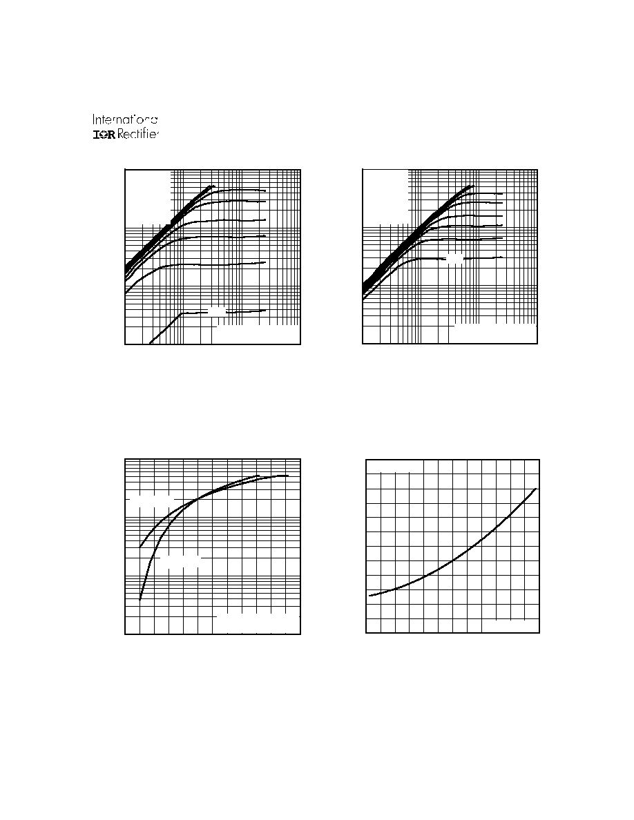
Fig 4. Normalized On-Resistance
Vs. Temperature
Fig 2. Typical Output Characteristics
Fig 1. Typical Output Characteristics
Fig 3. Typical Transfer Characteristics
1
10
100
1000
0.1
1
10
100
20µs PULSE WIDTH
T = 25 C
J
°
TOP
BOTTOM
VGS
15V
10V
8.0V
7.0V
6.0V
5.5V
5.0V
4.5V
V , Drain-to-Source Voltage (V)
I , Drain-to-Source Current (A)
DS
D
4.5V
1
10
100
1000
0.1
1
10
100
20µs PULSE WIDTH
T = 175 C
J
°
TOP
BOTTOM
VGS
15V
10V
8.0V
7.0V
6.0V
5.5V
5.0V
4.5V
V , Drain-to-Source Voltage (V)
I , Drain-to-Source Current (A)
DS
D
4.5V
1
10
100
1000
4.0
5.0
6.0
7.0
8.0
9.0
10.0
V = 50V
20µs PULSE WIDTH
DS
V , Gate-to-Source Voltage (V)
I , Drain-to-Source Current (A)
GS
D
T = 25 C
J
°
T = 175 C
J
°
-60 -40 -20
0
20 40 60 80 100 120 140 160 180
0.0
0.5
1.0
1.5
2.0
2.5
3.0
T , Junction Temperature ( C)
R , Drain-to-Source On Resistance
(Normalized)
J
DS(on)
°
V
=
I =
GS
D
10V
70A
IRFP064V
4
www.irf.com
Fig 8. Maximum Safe Operating Area
Fig 6. Typical Gate Charge Vs.
Gate-to-Source Voltage
Fig 5. Typical Capacitance Vs.
Drain-to-Source Voltage
Fig 7. Typical Source-Drain Diode
Forward Voltage
0
50
100
150
200
250
300
0
4
8
12
16
20
Q , Total Gate Charge (nC)
V , Gate-to-Source Voltage (V)
G
GS
FOR TEST CIRCUIT
SEE FIGURE
I =
D
13
130A
V
= 30V
DS
V
= 48V
DS
0.1
1
10
100
1000
0.0
0.4
0.8
1.2
1.6
2.0
2.4
V ,Source-to-Drain Voltage (V)
I , Reverse Drain Current (A)
SD
SD
V = 0 V
GS
T = 25 C
J
°
T = 175 C
J
°
1
10
100
VDS, Drain-to-Source Voltage (V)
0
2000
4000
6000
8000
10000
12000
C, Capacitance(pF)
Coss
Crss
Ciss
VGS = 0V, f = 1 MHZ
Ciss = Cgs + Cgd, Cds SHORTED
Crss = Cgd
Coss = Cds + Cgd
1
10
100
1000
VDS , Drain-toSource Voltage (V)
1
10
100
1000
10000
I D
, Drain-to-Source Current (A)
Tc = 25°C
Tj = 175°C
Single Pulse
1msec
10msec
OPERATION IN THIS AREA
LIMITED BY R DS(on)
100µsec
IRFP064V
www.irf.com
5
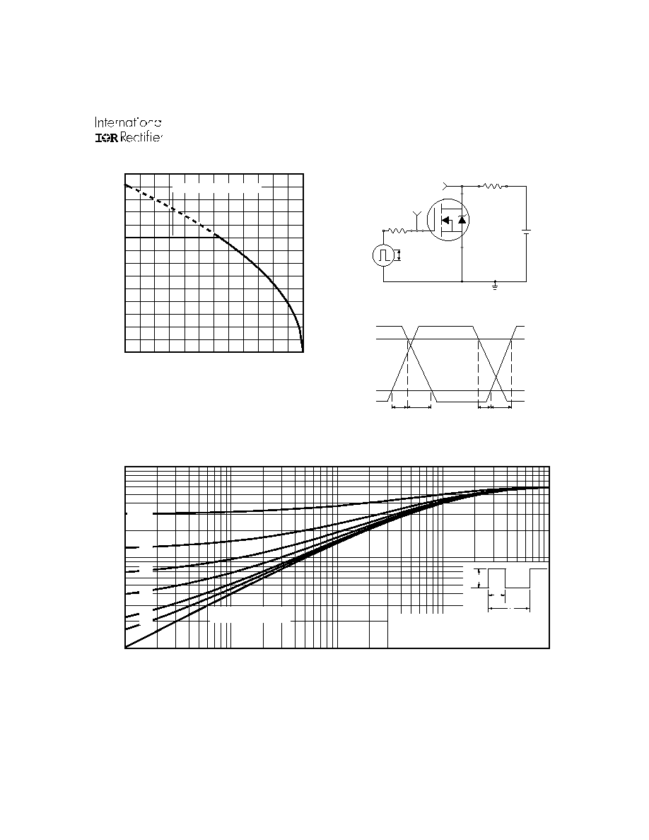
Fig 11. Maximum Effective Transient Thermal Impedance, Junction-to-Case
Fig 9. Maximum Drain Current Vs.
Case Temperature
0.01
0.1
1
0.00001
0.0001
0.001
0.01
0.1
Notes:
1. Duty factor D =
t / t
2. Peak T = P
x Z
+ T
1
2
J
DM
thJC
C
P
t
t
DM
1
2
t , Rectangular Pulse Duration (sec)
Thermal Response
(Z )
1
thJC
0.01
0.02
0.05
0.10
0.20
D = 0.50
SINGLE PULSE
(THERMAL RESPONSE)
25
50
75
100
125
150
175
0
20
40
60
80
100
120
140
T , Case Temperature
( C)
I , Drain Current (A)
°
C
D
LIMITED BY PACKAGE
V
DS
90%
10%
V
GS
t
d(on)
t
r
t
d(off)
t
f
V
DS
Pulse Width
1
µs
Duty Factor
0.1 %
R
D
V
GS
R
G
D.U.T.
V
GS
+
-
V
DD
Fig 10a. Switching Time Test Circuit
Fig 10b. Switching Time Waveforms