 | ÐлекÑÑоннÑй компоненÑ: IRFR2307Z | СкаÑаÑÑ:  PDF PDF  ZIP ZIP |
Äîêóìåíòàöèÿ è îïèñàíèÿ www.docs.chipfind.ru
10/20/04
www.irf.com
1
HEXFET
®
is a registered trademark of International Rectifier.
HEXFET
®
Power MOSFET
V
DSS
= 75V
R
DS(on)
= 16m
I
D
= 42A
Specifically designed for Automotive applications,
this HEXFET
®
Power MOSFET utilizes the latest
processing techniques to achieve extremely low
on-resistance per silicon area. Additional features
of this design are a 175°C junction operating
temperature, fast switching speed and improved
repetitive avalanche rating . These features com-
bine to make this design an extremely efficient and
reliable device for use in Automotive applications
and a wide variety of other applications.
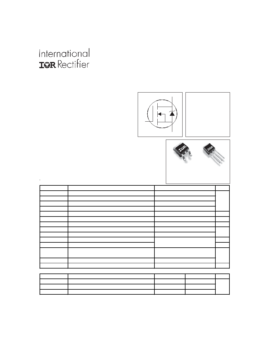
S
D
G
Description
l
Advanced Process Technology
l
Ultra Low On-Resistance
l
175°C Operating Temperature
l
Fast Switching
l
Repetitive Avalanche Allowed up to Tjmax
Features
D-Pak
IRFR2307Z
I-Pak
IRFU2307Z
AUTOMOTIVE MOSFET
PD - 96910
IRFR2307Z
IRFU2307Z
Absolute Maximum Ratings
Parameter
Units
I
D
@ T
C
= 25°C Continuous Drain Current, V
GS
@ 10V
(Silicon Limited)
I
D
@ T
C
= 100°C Continuous Drain Current, V
GS
@ 10V
A
I
D
@ T
C
= 25°C Continuous Drain Current, V
GS
@ 10V
(Package Limited)
I
DM
Pulsed Drain Current
P
D
@T
C
= 25°C Power Dissipation
W
Linear Derating Factor
W/°C
V
GS
Gate-to-Source Voltage
V
E
AS (Thermally limited)
Single Pulse Avalanche Energy
d
mJ
E
AS
(Tested )
Single Pulse Avalanche Energy Tested Value
h
I
AR
Avalanche Current
Ã
A
E
AR
Repetitive Avalanche Energy
g
mJ
T
J
Operating Junction and
T
STG
Storage Temperature Range
°C
Soldering Temperature, for 10 seconds
Mounting Torque, 6-32 or M3 screw
Thermal Resistance
Parameter
Typ.
Max.
Units
R
JC
Junction-to-Case
j
1.42
R
JA
Junction-to-Ambient (PCB mount)
ij
40
°C/W
R
JA
Junction-to-Ambient
j
110
-55 to + 175
300 (1.6mm from case )
10 lbf
yin (1.1Nym)
110
0.70
± 20
Max.
53
38
210
42
140
100
See Fig.12a, 12b, 15, 16
IRFR/U2307Z
2
www.irf.com
S
D
G
Electrical Characteristics @ T
J
= 25°C (unless otherwise specified)
Parameter
Min. Typ. Max. Units
V
(BR)DSS
Drain-to-Source Breakdown Voltage
75
V
V
(BR)DSS
/
T
J
Breakdown Voltage Temp. Coefficient
0.072
V/°C
R
DS(on)
Static Drain-to-Source On-Resistance
12.8
16
m
V
GS(th)
Gate Threshold Voltage
2.0
4.0
V
gfs
Forward Transconductance
30
S
I
DSS
Drain-to-Source Leakage Current
25
µA
250
I
GSS
Gate-to-Source Forward Leakage
200
nA
Gate-to-Source Reverse Leakage
-200
Q
g
Total Gate Charge
50
75
Q
gs
Gate-to-Source Charge
14
nC
Q
gd
Gate-to-Drain ("Miller") Charge
19
t
d(on)
Turn-On Delay Time
16
t
r
Rise Time
65
t
d(off)
Turn-Off Delay Time
44
ns
t
f
Fall Time
29
L
D
Internal Drain Inductance
4.5
Between lead,
nH
6mm (0.25in.)
L
S
Internal Source Inductance
7.5
from package
and center of die contact
C
iss
Input Capacitance
2190
C
oss
Output Capacitance
280
C
rss
Reverse Transfer Capacitance
150
pF
C
oss
Output Capacitance
1070
C
oss
Output Capacitance
190
C
oss
eff.
Effective Output Capacitance
400
Source-Drain Ratings and Characteristics
Parameter
Min. Typ. Max. Units
I
S
Continuous Source Current
42
(Body Diode)
A
I
SM
Pulsed Source Current
210
(Body Diode)
Ã
V
SD
Diode Forward Voltage
1.3
V
t
rr
Reverse Recovery Time
31
47
ns
Q
rr
Reverse Recovery Charge
31
47
nC
t
on
Forward Turn-On Time
Intrinsic turn-on time is negligible (turn-on is dominated by LS+LD)
V
GS
= 10V
e
V
DD
= 38V
I
D
= 32A
R
G
= 10
T
J
= 25°C, I
S
= 32A, V
GS
= 0V
e
T
J
= 25°C, I
F
= 32A, V
DD
= 38V
di/dt = 100A/µs
e
Conditions
V
GS
= 0V, I
D
= 250µA
Reference to 25°C, I
D
= 1mA
V
GS
= 10V, I
D
= 32A
e
V
DS
= V
GS
, I
D
= 100µA
V
DS
= 75V, V
GS
= 0V
V
DS
= 75V, V
GS
= 0V, T
J
= 125°C
MOSFET symbol
showing the
integral reverse
p-n junction diode.
Conditions
V
GS
= 10V
e
V
GS
= 0V
V
DS
= 25V
= 1.0MHz
V
GS
= 0V, V
DS
= 1.0V, = 1.0MHz
V
GS
= 0V, V
DS
= 60V, = 1.0MHz
V
GS
= 0V, V
DS
= 0V to 60V
f
V
GS
= 20V
V
GS
= -20V
V
DS
= 60V
V
DS
= 25V, I
D
= 32A
I
D
= 32A
IRFR/U2307Z
www.irf.com
3
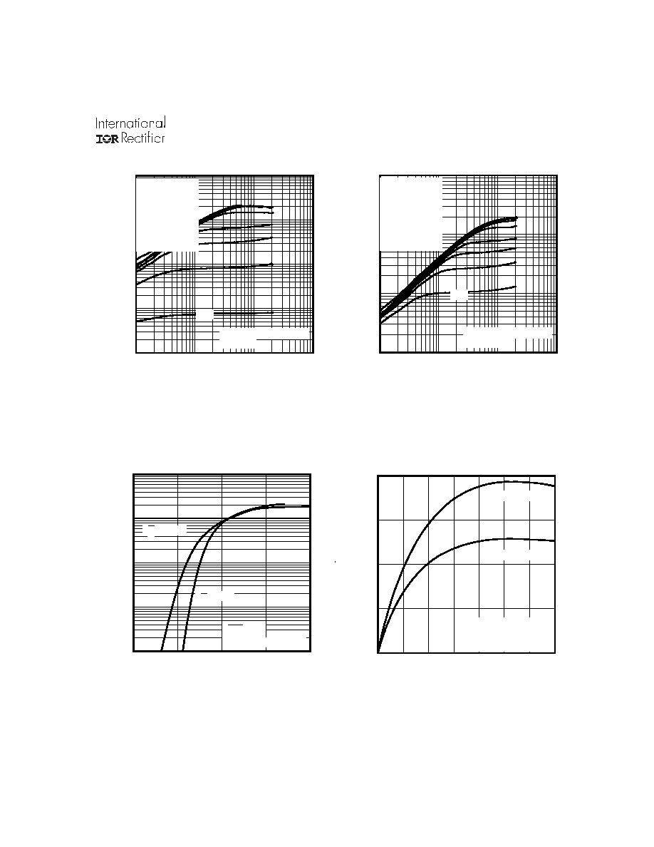
Fig 2. Typical Output Characteristics
Fig 1. Typical Output Characteristics
Fig 3. Typical Transfer Characteristics
Fig 4. Typical Forward Transconductance
vs. Drain Current
0.1
1
10
100
VDS, Drain-to-Source Voltage (V)
1
10
100
1000
I D
,
D
r
a
i
n
-
t
o
-
S
o
u
r
c
e
C
u
r
r
e
n
t
(
A
)
VGS
TOP 15V
10V
8.0V
7.0V
6.0V
5.5V
5.0V
BOTTOM
4.5V
60µs PULSE WIDTH
Tj = 175°C
4.5V
2
4
6
8
10
VGS, Gate-to-Source Voltage (V)
0.1
1
10
100
1000
I D
,
D
r
a
i
n
-
t
o
-
S
o
u
r
c
e
C
u
r
r
e
n
t
(
)
TJ = 25°C
TJ = 175°C
VDS = 20V
60µs PULSE WIDTH
0
10
20
30
40
50
60
70
ID,Drain-to-Source Current (A)
0
20
40
60
80
G
f
s,
F
o
r
w
a
r
d
T
r
a
n
s
c
o
n
d
u
c
t
a
n
c
e
(
S
)
TJ = 25°C
TJ = 175°C
VDS = 10V
380µs PULSE WIDTH
0.1
1
10
100
VDS, Drain-to-Source Voltage (V)
0.1
1
10
100
1000
I D
,
D
r
a
i
n
-
t
o
-
S
o
u
r
c
e
C
u
r
r
e
n
t
(
A
)
VGS
TOP 15V
10V
8.0V
7.0V
6.0V
5.5V
5.0V
BOTTOM
4.5V
60µs PULSE WIDTH
Tj = 25°C
4.5V
IRFR/U2307Z
4
www.irf.com
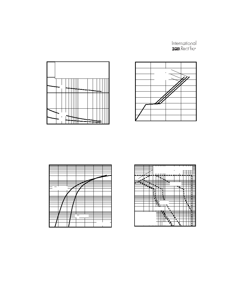
Fig 8. Maximum Safe Operating Area
Fig 6. Typical Gate Charge vs.
Gate-to-Source Voltage
Fig 5. Typical Capacitance vs.
Drain-to-Source Voltage
Fig 7. Typical Source-Drain Diode
Forward Voltage
0.2
0.4
0.6
0.8
1.0
1.2
1.4
1.6
VSD, Source-to-Drain Voltage (V)
0.10
1.00
10.00
100.00
1000.00
I S
D
,
R
e
v
e
r
s
e
D
r
a
i
n
C
u
r
r
e
n
t
(
A
)
TJ = 25°C
TJ = 175°C
VGS = 0V
1
10
100
VDS, Drain-to-Source Voltage (V)
0
1000
2000
3000
4000
C
,
C
a
p
a
c
i
t
a
n
c
e
(
p
F
)
VGS = 0V, f = 1 MHZ
Ciss = Cgs + Cgd, Cds SHORTED
Crss = Cgd
Coss = Cds + Cgd
Coss
Crss
Ciss
0
20
40
60
80
QG Total Gate Charge (nC)
0
4
8
12
16
20
V
G
S
,
G
a
t
e
-
t
o
-
S
o
u
r
c
e
V
o
l
t
a
g
e
(
V
)
VDS= 60V
VDS= 38V
VDS= 15V
ID= 32A
1
10
100
VDS , Drain-toSource Voltage (V)
0.1
1
10
100
1000
I D
,
D
r
a
i
n
-
t
o
-
S
o
u
r
c
e
C
u
r
r
e
n
t
(
A
)
Tc = 25°C
Tj = 175°C
Single Pulse
1msec
10msec
OPERATION IN THIS AREA
LIMITED BY RDS(on)
100µsec
DC
IRFR/U2307Z
www.irf.com
5
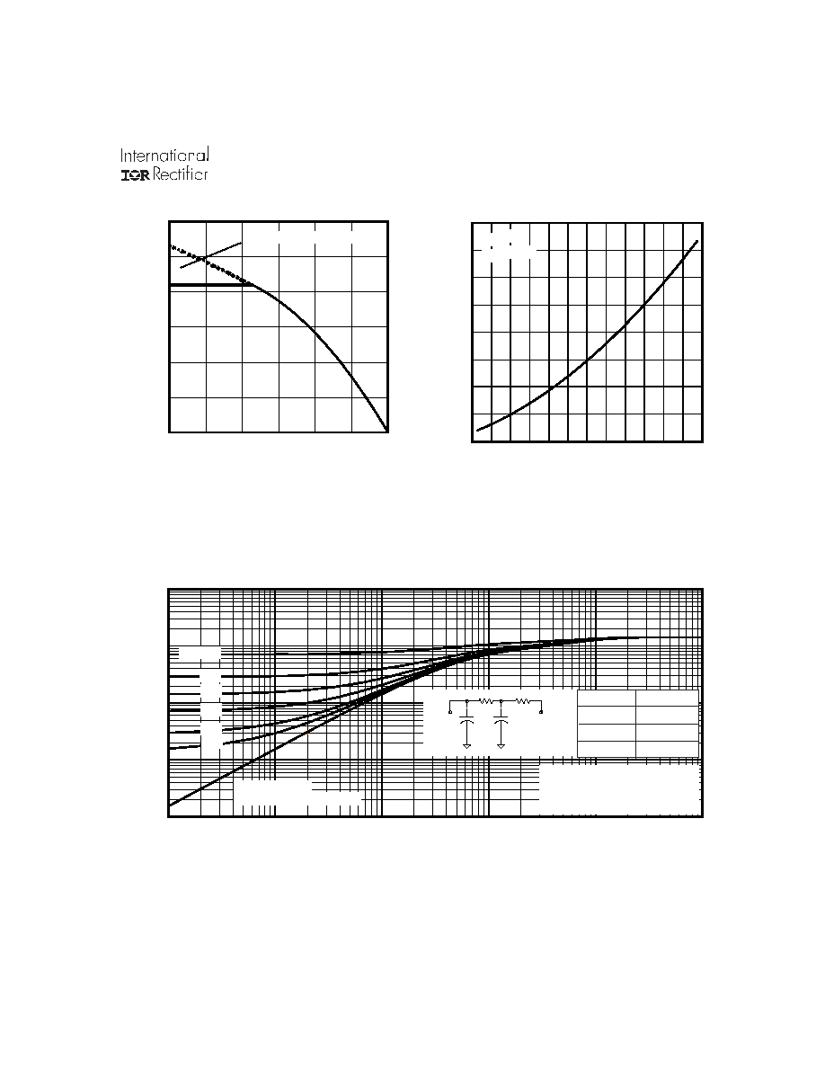
Fig 11. Maximum Effective Transient Thermal Impedance, Junction-to-Case
Fig 9. Maximum Drain Current vs.
Case Temperature
Fig 10. Normalized On-Resistance
vs. Temperature
-60 -40 -20 0
20 40 60 80 100 120 140 160 180
TJ , Junction Temperature (°C)
0.5
1.0
1.5
2.0
2.5
R
D
S
(
o
n
)
,
D
r
a
i
n
-
t
o
-
S
o
u
r
c
e
O
n
R
e
s
i
s
t
a
n
c
e
(
N
o
r
m
a
l
i
z
e
d
)
ID = 32A
VGS = 10V
1E-006
1E-005
0.0001
0.001
0.01
0.1
t1 , Rectangular Pulse Duration (sec)
0.001
0.01
0.1
1
10
T
h
e
r
m
a
l
R
e
s
p
o
n
s
e
(
Z
t
h
J
C
)
0.20
0.10
D = 0.50
0.02
0.01
0.05
SINGLE PULSE
( THERMAL RESPONSE )
Notes:
1. Duty Factor D = t1/t2
2. Peak Tj = P dm x Zthjc + Tc
Ri (°C/W)
i (sec)
0.7938 0.000499
0.6257 0.005682
J
J
1
1
2
2
R
1
R
1
R
2
R
2
C
Ci i
/Ri
Ci=
i/Ri
25
50
75
100
125
150
175
TC , Case Temperature (°C)
0
10
20
30
40
50
60
I D
,
D
r
a
i
n
C
u
r
r
e
n
t
(
A
)
LIMITED BY PACKAGE