 | ÐлекÑÑоннÑй компоненÑ: IRFR5305 | СкаÑаÑÑ:  PDF PDF  ZIP ZIP |
Äîêóìåíòàöèÿ è îïèñàíèÿ www.docs.chipfind.ru
IRFR/U5305
HEXFET
®
Power MOSFET
Fifth Generation HEXFETs from International Rectifier utilize
advanced processing techniques to achieve extremely low
on-resistance per silicon area. This benefit, combined with
the fast switching speed and ruggedized device design that
HEXFET
®
Power MOSFETs are well known for, provides
the designer with an extremely efficient and reliable device
for use in a wide variety of applications.
The D-Pak is designed for surface mounting using vapor
phase, infrared, or wave soldering techniques. The straight
lead version (IRFU series) is for through-hole mounting
applications. Power dissipation levels up to 1.5 watts are
possible in typical surface mount applications.
Parameter
Max.
Units
I
D
@ T
C
= 25°C
Continuous Drain Current, V
GS
@ -10V
-31
I
D
@ T
C
= 100°C
Continuous Drain Current, V
GS
@ -10V
-22
A
I
DM
Pulsed Drain Current
-110
P
D
@T
C
= 25°C
Power Dissipation
110
W
Linear Derating Factor
0.71
W/°C
V
GS
Gate-to-Source Voltage
± 20
V
E
AS
Single Pulse Avalanche Energy
280
mJ
I
AR
Avalanche Current
-16
A
E
AR
Repetitive Avalanche Energy
11
mJ
dv/dt
Peak Diode Recovery dv/dt
-5.0
V/ns
T
J
Operating Junction and
-55 to + 175
T
STG
Storage Temperature Range
Soldering Temperature, for 10 seconds
300 (1.6mm from case )
°C
Mounting torque, 6-32 or M3 srew
10 lbf·in (1.1N·m)
Absolute Maximum Ratings
Parameter
Typ.
Max.
Units
R
JC
Junction-to-Case
1.4
R
JA
Junction-to-Ambient (PCB mount)*
50
°C/W
R
JA
Junction-to-Ambient**
110
Thermal Resistance
V
DSS
= -55V
R
DS(on)
= 0.065
I
D
= -31A
l
Ultra Low On-Resistance
l
Surface Mount (IRFR5305)
l
Straight Lead (IRFU5305)
l
Advanced Process Technology
l
Fast Switching
l
Fully Avalanche Rated
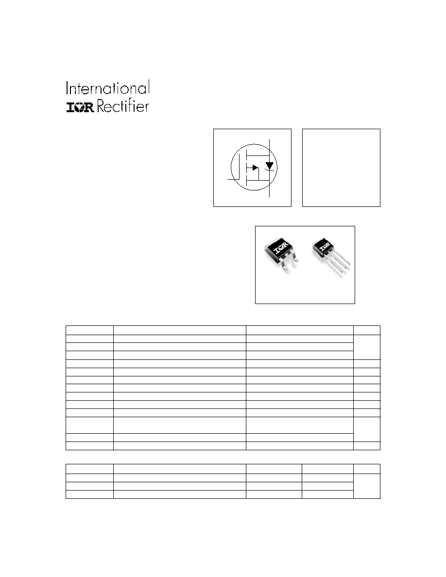
Description
10/23/00
S
D
G
D-Pak I-Pak
IRFR5305 IRFU5305
PD - 91402A
IRFR/U5305
2
www.irf.com
Parameter
Min. Typ. Max.
Units
Conditions
I
S
Continuous Source Current
MOSFET symbol
(Body Diode)
showing the
I
SM
Pulsed Source Current
integral reverse
(Body Diode)
p-n junction diode.
V
SD
Diode Forward Voltage
-1.3
V
T
J
= 25°C, I
S
= -16A, V
GS
= 0V
t
rr
Reverse Recovery Time
71
110
ns
T
J
= 25°C, I
F
= -16A
Q
rr
Reverse RecoveryCharge
170
250
nC
di/dt = -100A/µs
Source-Drain Ratings and Characteristics
Parameter
Min. Typ. Max. Units
Conditions
V
(BR)DSS
Drain-to-Source Breakdown Voltage
-55
V
V
GS
= 0V, I
D
= -250µA
V
(BR)DSS
/
T
J
Breakdown Voltage Temp. Coefficient
-0.034
V/°C
Reference to 25°C, I
D
= -1mA
R
DS(on)
Static Drain-to-Source On-Resistance
0.065
V
GS
= -10V, I
D
= -16A
V
GS(th)
Gate Threshold Voltage
-2.0
-4.0
V
V
DS
= V
GS
, I
D
= -250µA
g
fs
Forward Transconductance
8.0
S
V
DS
= -25V, I
D
= -16A
-25
µA
V
DS
= -55V, V
GS
= 0V
-250
V
DS
= -44V, V
GS
= 0V, T
J
= 150°C
Gate-to-Source Forward Leakage
100
V
GS
= 20V
Gate-to-Source Reverse Leakage
-100
nA
V
GS
= -20V
Q
g
Total Gate Charge
63
I
D
= -16A
Q
gs
Gate-to-Source Charge
13
nC
V
DS
= -44V
Q
gd
Gate-to-Drain ("Miller") Charge
29
V
GS
= -10V, See Fig. 6 and 13
t
d(on)
Turn-On Delay Time
14
V
DD
= -28V
t
r
Rise Time
66
I
D
= -16A
t
d(off)
Turn-Off Delay Time
39
R
G
= 6.8
t
f
Fall Time
63
R
D
= 1.6
,
See Fig. 10
Between lead,
6mm (0.25in.)
from package
and center of die contact
C
iss
Input Capacitance
1200
V
GS
= 0V
C
oss
Output Capacitance
520
pF
V
DS
= -25V
C
rss
Reverse Transfer Capacitance
250
= 1.0MHz, See Fig. 5
nH
Electrical Characteristics @ T
J
= 25°C (unless otherwise specified)
L
D
Internal Drain Inductance
L
S
Internal Source Inductance
I
GSS
ns
4.5
7.5
I
DSS
Drain-to-Source Leakage Current
Repetitive rating; pulse width limited by
max. junction temperature. (See Fig. 11)
I
SD
-16A, di/dt
-280A/µs, V
DD
V
(BR)DSS
,
T
J
175°C
Notes:
V
DD
= -25V, starting T
J
= 25°C, L = 2.1mH
R
G
= 25
, I
AS
= -16A. (See Figure 12)
Pulse width
300µs; duty cycle
2%.
-31
-110
A
S
D
G
S
D
G
This is applied for I-PAK, L
S
of D-PAK is measured between
lead and center of die contact.
Uses IRF5305 data and test conditions.
* When mounted on 1" square PCB (FR-4 or G-10 Material).
For recommended footprint and soldering techniques refer to application note #AN-994.
** Uses typical socket mount.
IRFR/U5305
www.irf.com
3
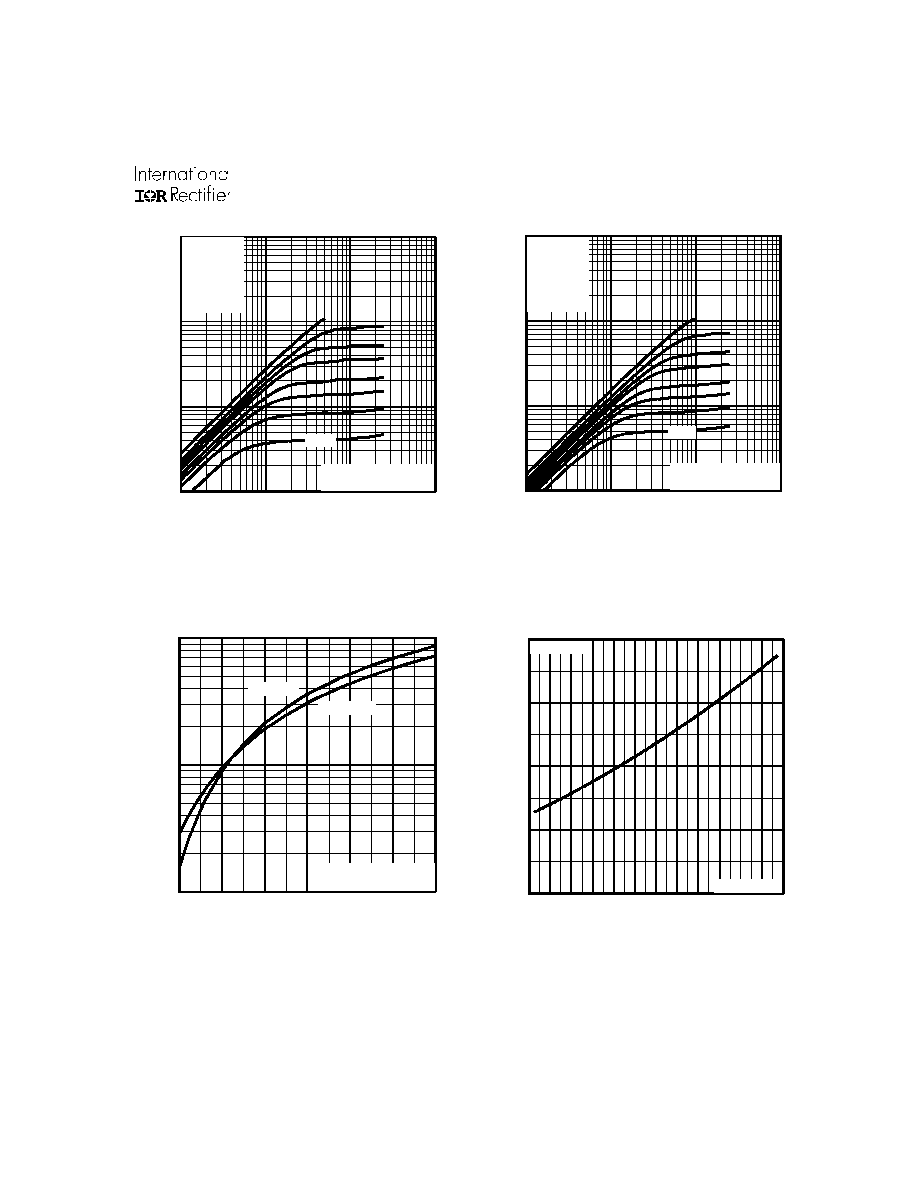
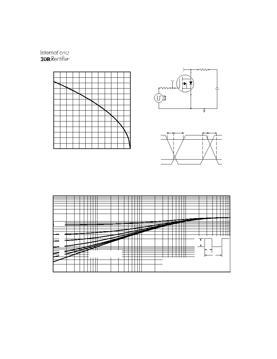
Fig 4. Normalized On-Resistance
Vs. Temperature
Fig 2. Typical Output Characteristics
Fig 1. Typical Output Characteristics
Fig 3. Typical Transfer Characteristics
1
1 0
1 0 0
1 0 0 0
0 . 1
1
1 0
1 0 0
D
D S
2 0µ s P U LS E W ID T H
T = 2 5°C
c
A
-I
,
D
r
a
i
n
-
t
o
-S
o
u
rc
e
C
u
rre
n
t
(A
)
-V , D rain-to-S ourc e V olta ge (V )
VGS
TO P - 15V
- 10V
- 8.0V
- 7.0V
- 6.0V
- 5.5V
- 5.0V
BOT TOM - 4.5V
-4.5 V
1
1 0
1 0 0
1 0 0 0
0.1
1
1 0
1 0 0
D
D S
A
-I
,
D
r
a
i
n
-
t
o
-S
o
u
r
c
e
C
u
rre
n
t
(A
)
-V , D rain-to-S ource V oltage (V )
VGS
TOP - 15V
- 10V
- 8.0V
- 7.0V
- 6.0V
- 5.5V
- 5.0V
BOTTOM - 4.5V
-4 .5 V
20 µ s P U L S E W ID T H
T = 17 5°C
C
1
1 0
1 0 0
4
5
6
7
8
9
1 0
T = 2 5°C
J
T = 17 5 °C
J
A
V = -2 5 V
2 0µ s P U L S E W ID TH
DS
G S
-V , G ate -to-S ource V olta ge (V )
D
-I
,
D
r
a
i
n
-
t
o
-S
o
u
rc
e
C
u
rre
n
t
(A
)
0 . 0
0 . 5
1 . 0
1 . 5
2 . 0
- 6 0
- 4 0
- 2 0
0
2 0
4 0
6 0
8 0
1 0 0 1 2 0 1 4 0 1 6 0 1 8 0
J
T , Junction T em perature (°C )
R
, D
r
a
i
n
-
to
-
S
o
u
r
c
e
O
n
R
e
s
i
s
ta
n
c
e
D
S
(
on)
(N
o
r
m
a
l
i
z
e
d
)
A
I = -27 A
V = -10 V
D
G S
J
J
IRFR/U5305
4
www.irf.com
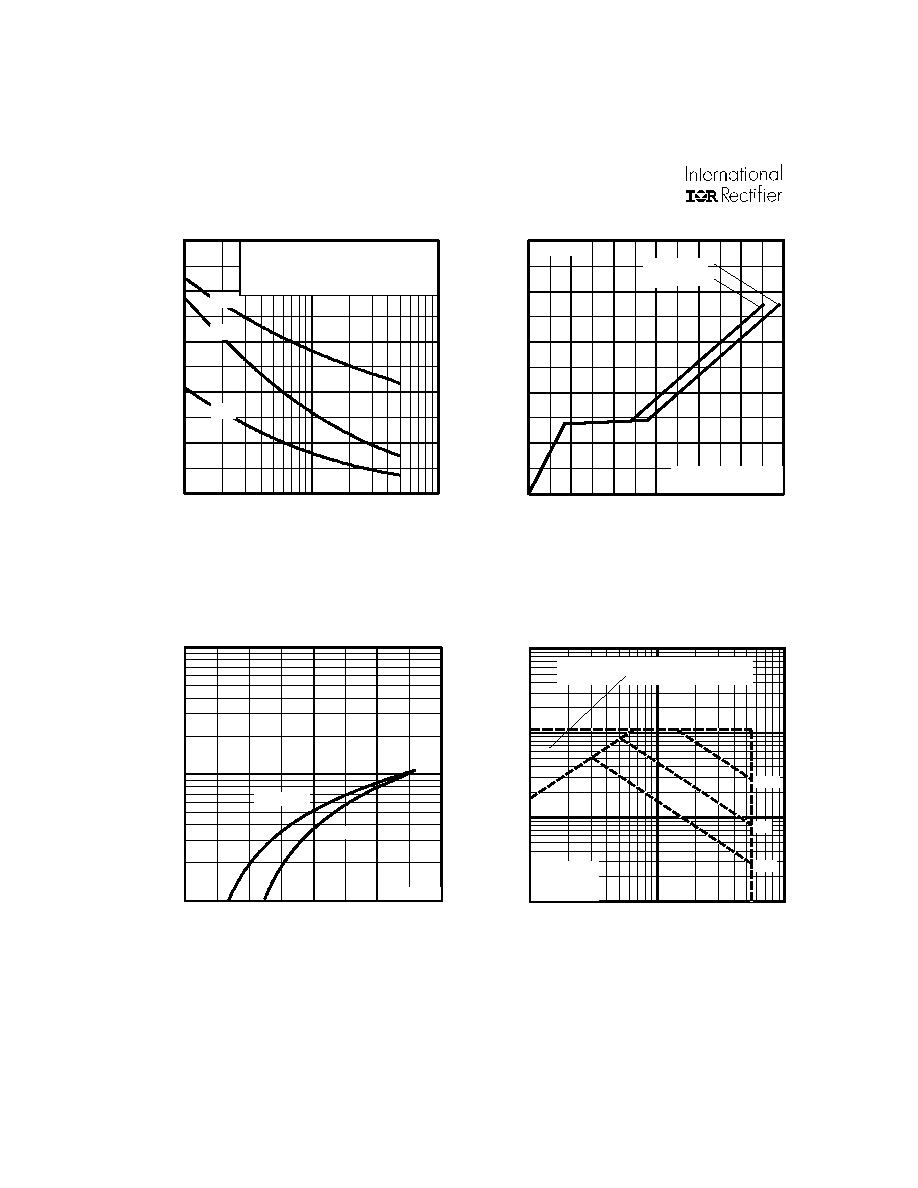
Fig 8. Maximum Safe Operating Area
Fig 6. Typical Gate Charge Vs.
Gate-to-Source Voltage
Fig 5. Typical Capacitance Vs.
Drain-to-Source Voltage
Fig 7. Typical Source-Drain Diode
Forward Voltage
0
5 0 0
1 0 0 0
1 5 0 0
2 0 0 0
2 5 0 0
1
1 0
1 0 0
C
,
C
a
p
a
c
i
t
anc
e (
p
F
)
A
V = 0V , f = 1 M H z
C = C + C , C S H O R TE D
C = C
C = C + C
G S
iss g s g d d s
rs s g d
o ss ds g d
C
is s
C
os s
C
rs s
D S
-V , D rain-to -S o urc e V oltag e (V )
0
4
8
1 2
1 6
2 0
0
1 0
2 0
3 0
4 0
5 0
6 0
Q , Total G ate C harge (nC )
G
A
F O R TE S T C IR C U IT
S E E F IG U R E 1 3
V = -4 4V
V = -2 8V
I = -1 6A
GS
-
V
, G
a
te
-
t
o
-
S
o
u
r
c
e
V
o
l
t
a
g
e
(
V
)
D
D S
D S
1 0
1 0 0
1 0 0 0
0 . 4
0 . 8
1 . 2
1 . 6
2 . 0
T = 25 °C
J
V = 0V
G S
S D
SD
A
-I
,
R
e
v
e
rs
e
D
r
a
i
n
C
u
rre
n
t
(A
)
-V , S o urc e-to -D ra in V o lta ge (V )
T = 17 5 °C
J
1
1 0
1 0 0
1 0 0 0
1
1 0
1 0 0
O P E R A T IO N IN T H IS A R E A L IM ITE D
B Y R
D S (o n)
1 0 0 µ s
1 m s
1 0 m s
A
T = 25 °C
T = 17 5°C
S ing le P u ls e
C
J
D S
-V , D rain-to-S ourc e V oltage (V )
D
-I
,
D
r
a
i
n
C
u
rre
n
t
(A
)
IRFR/U5305
www.irf.com
5
Fig 10a. Switching Time Test Circuit
Fig 10b. Switching Time Waveforms
Fig 11. Maximum Effective Transient Thermal Impedance, Junction-to-Case
Fig 9. Maximum Drain Current Vs.
Case Temperature
V
DS
-10V
Pulse Width
1
µs
Duty Factor
0.1 %
R
D
V
GS
V
DD
R
G
D.U.T.
V
DS
90%
10%
V
GS
t
d(on)
t
r
t
d(off)
t
f
+
-
25
50
75
100
125
150
175
0
5
10
15
20
25
30
35
T , Case Temperature ( C)
-I , Drain Current (A)
°
C
D
0.01
0.1
1
10
0.00001
0.0001
0.001
0.01
0.1
Notes:
1. Duty factor D = t / t
2. Peak T = P
x Z
+ T
1
2
J
DM
thJC
C
P
t
t
DM
1
2
t , Rectangular Pulse Duration (sec)
Thermal Response
(Z )
1
thJC
0.01
0.02
0.05
0.10
0.20
D = 0.50
SINGLE PULSE
(THERMAL RESPONSE)
IRFR/U5305
6
www.irf.com
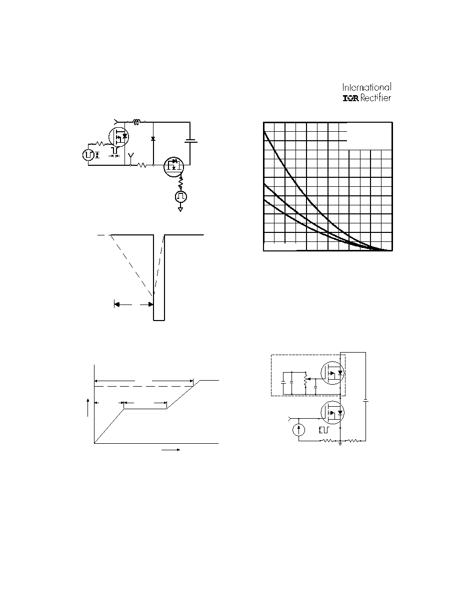
Fig 13b. Gate Charge Test Circuit
Fig 13a. Basic Gate Charge Waveform
Fig 12c. Maximum Avalanche Energy
Vs. Drain Current
Q
G
Q
GS
Q
GD
V
G
Charge
-10V
D.U.T.
V
DS
I
D
I
G
-3mA
V
GS
.3
µ
F
50K
.2
µ
F
12V
Current Regulator
Same Type as D.U.T.
Current Sampling Resistors
+
-
0
1 0 0
2 0 0
3 0 0
4 0 0
5 0 0
6 0 0
7 0 0
2 5
5 0
7 5
1 0 0
1 2 5
1 5 0
1 7 5
J
E
,
S
i
n
g
l
e
P
u
l
s
e
A
v
a
lanc
he E
n
er
gy
(
m
J
)
AS
A
S ta rtin g T , J u nc tio n T e m pe ra tu re (°C )
V = -2 5V
I
TO P -6.6 A
-11 A
B O T T O M -1 6A
D D
D
Fig 12b. Unclamped Inductive Waveforms
Fig 12a. Unclamped Inductive Test
Circuit
tp
V
(BR)DSS
I
A S
R
G
IA S
0 .0 1
tp
D .U .T
L
V D S
+
-
VD D
D R IV E R
A
- 2 0 V
1 5 V
IRFR/U5305
www.irf.com
7
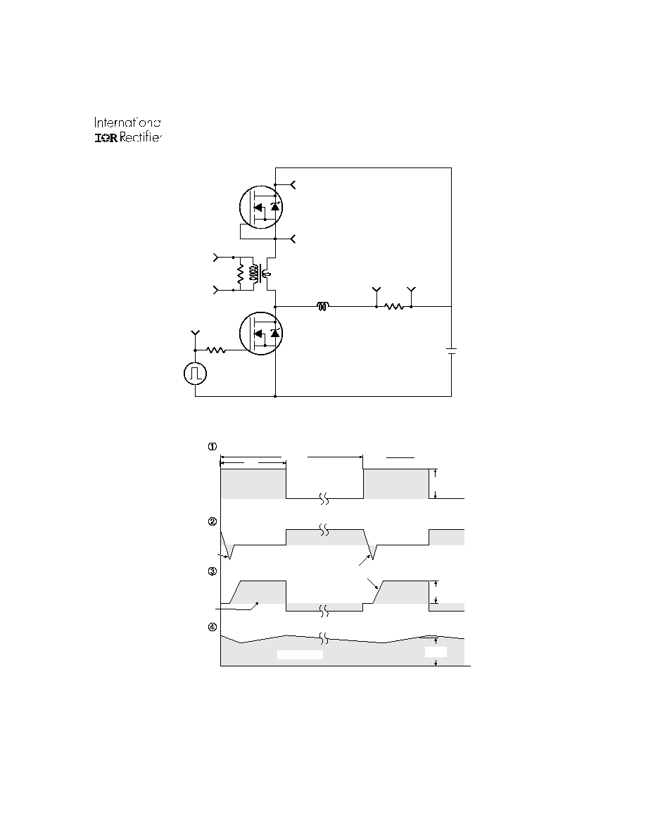
Peak Diode Recovery dv/dt Test Circuit
P.W.
Period
di/dt
Diode Recovery
dv/dt
Ripple
5%
Body Diode
Forward Drop
Re-Applied
Voltage
Reverse
Recovery
Current
Body Diode Forward
Current
V
GS
=10V
V
DD
I
SD
Driver Gate Drive
D.U.T. I
SD
Waveform
D.U.T. V
DS
Waveform
Inductor Curent
D =
P.W.
Period
+
-
+
+
+
-
-
-
R
G
V
DD
·
dv/dt controlled by R
G
·
I
SD
controlled by Duty Factor "D"
·
D.U.T. - Device Under Test
D.U.T
Circuit Layout Considerations
·
Low Stray Inductance
·
Ground Plane
·
Low Leakage Inductance
Current Transformer
*
Reverse Polarity for P-Channel
** Use P-Channel Driver for P-Channel Measurements
*
V
GS
*
**
[ ]
[ ]
***
V
GS
= 5.0V for Logic Level and 3V Drive Devices
[ ] ***
Fig 14. For P-Channel HEXFETS
IRFR/U5305
8
www.irf.com
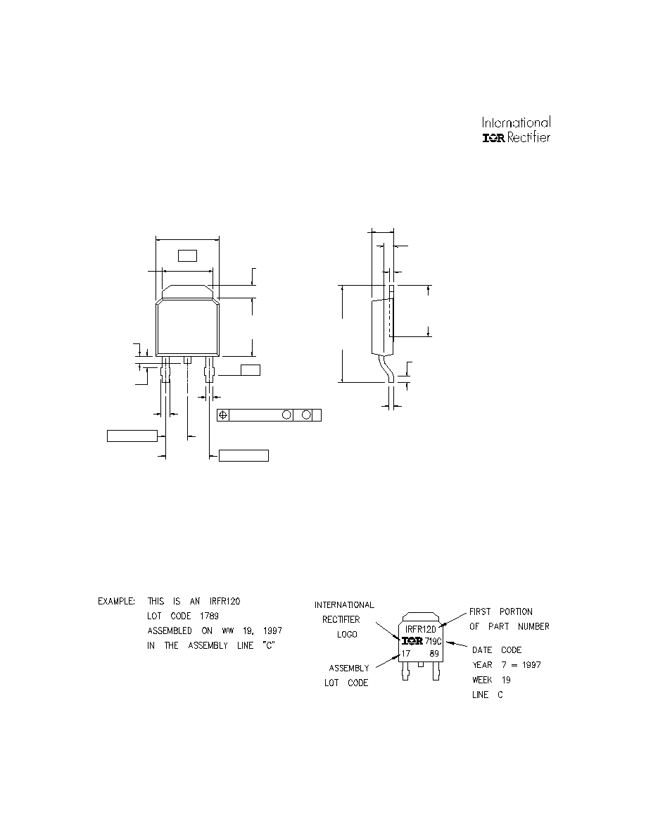
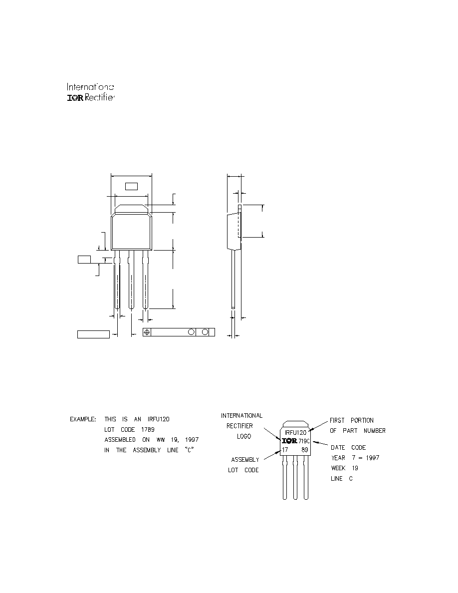
D-Pak (TO-252AA) Package Outline
Dimensions are shown in millimeters (inches)
D-Pak (TO-252AA) Part Marking Information
6 .7 3 (.2 6 5 )
6 .3 5 (.2 5 0 )
- A -
4
1 2 3
6 .2 2 (.2 4 5 )
5 .9 7 (.2 3 5 )
- B -
3 X
0 .8 9 (.0 3 5 )
0 .6 4 (.0 2 5 )
0 .2 5 ( .0 1 0 ) M A M B
4 .5 7 ( .1 8 0 )
2 .2 8 ( .0 9 0 )
2 X
1 .1 4 (.0 4 5 )
0 .7 6 (.0 3 0 )
1 .5 2 ( .0 6 0 )
1 .1 5 ( .0 4 5 )
1.0 2 (.0 4 0 )
1.6 4 (.0 2 5 )
5 .4 6 (.2 1 5 )
5 .2 1 (.2 0 5 )
1 .2 7 (.0 5 0 )
0 .8 8 (.0 3 5 )
2 .3 8 (.0 9 4 )
2 .1 9 (.0 8 6 )
1 .1 4 (.0 4 5 )
0 .8 9 (.0 3 5 )
0 .5 8 (.0 2 3 )
0 .4 6 (.0 1 8 )
6 .4 5 (.2 4 5 )
5 .6 8 (.2 2 4 )
0 .5 1 (.0 2 0 )
M IN .
0 .5 8 ( .0 2 3 )
0 .4 6 ( .0 1 8 )
L E A D A S S IG N M E N T S
1 - G A T E
2 - D R A IN
3 - S O U R C E
4 - D R A IN
1 0 .4 2 (.4 1 0 )
9 .4 0 (.3 7 0 )
N O T E S :
1 D IM E N S IO N IN G & T O L E R A N C IN G P E R A N S I Y 1 4 .5 M , 1 9 8 2 .
2 C O N T R O L L IN G D IM E N S IO N : IN C H .
3 C O N F O R M S T O J E D E C O U T L IN E T O - 2 5 2 A A .
4 D IM E N S IO N S S H O W N A R E B E F O R E S O L D E R D IP ,
S O L D E R D IP M A X. + 0 .1 6 (.0 0 6 ) .
IRFR/U5305
www.irf.com
9
I-Pak (TO-251AA) Package Outline
Dimensions are shown in millimeters (inches)
I-Pak (TO-251AA) Part Marking Information
6 .7 3 (.26 5 )
6 .3 5 (.25 0 )
- A -
6 .2 2 ( .2 4 5 )
5 .9 7 ( .2 3 5 )
- B -
3 X
0 .8 9 (.0 35 )
0 .6 4 (.0 25 )
0 .2 5 (.0 1 0 ) M A M B
2 .28 (.0 9 0 )
1 .1 4 (.0 45 )
0 .7 6 (.0 30 )
5 .4 6 (.2 1 5 )
5 .2 1 (.2 0 5 )
1 .2 7 ( .0 5 0 )
0 .8 8 ( .0 3 5 )
2 .3 8 (.0 9 4 )
2 .1 9 (.0 8 6 )
1 .1 4 ( .0 4 5 )
0 .8 9 ( .0 3 5 )
0 .5 8 (.0 2 3 )
0 .4 6 (.0 1 8 )
L E A D A S S IG N M E N T S
1 - G A T E
2 - D R A IN
3 - S O U R C E
4 - D R A IN
N O T E S :
1 D IM E N S IO N IN G & T O L E R A N C IN G P E R A N S I Y 1 4 .5M , 19 8 2 .
2 C O N T R O L L IN G D IM E N S IO N : IN C H .
3 C O N F O R M S T O J E D E C O U T L IN E T O -2 5 2 A A .
4 D IM E N S IO N S S H O W N A R E B E F O R E S O L D E R D IP ,
S O L D E R D IP M A X. + 0.1 6 (.0 0 6 ).
9 .6 5 ( .3 8 0 )
8 .8 9 ( .3 5 0 )
2 X
3 X
2.2 8 (.0 9 0)
1.9 1 (.0 7 5)
1 .5 2 (.0 6 0 )
1 .1 5 (.0 4 5 )
4
1 2 3
6 .4 5 (.2 4 5 )
5 .6 8 (.2 2 4 )
0 .5 8 (.0 2 3 )
0 .4 6 (.0 1 8 )
IRFR/U5305
10
www.irf.com
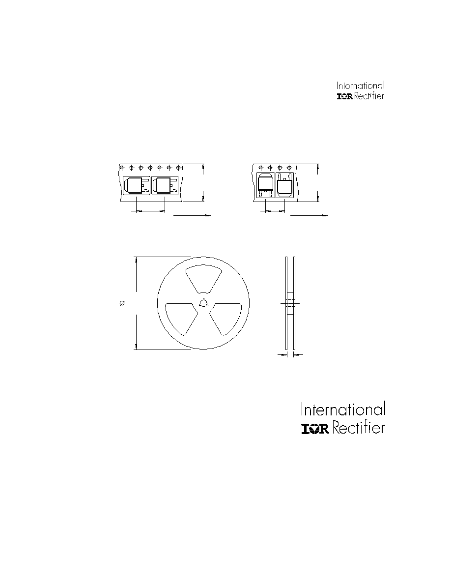
T R
1 6 .3 ( .6 4 1 )
1 5 .7 ( .6 1 9 )
8 .1 ( .3 18 )
7 .9 ( .3 12 )
1 2 .1 ( .4 7 6 )
1 1 .9 ( .4 6 9 )
F E E D D IR E C T IO N
F E E D D IR E C T IO N
1 6 .3 ( .64 1 )
1 5 .7 ( .61 9 )
T R R
T R L
N O T ES :
1 . C O N T R O L L IN G D IM EN S IO N : M IL L IM ET E R .
2 . AL L D IM EN SIO N S AR E SH O W N IN M IL L IM ET E R S ( IN C H E S ).
3 . O U T L IN E C O N F O R M S T O E IA -4 81 & E IA -54 1 .
N O T ES :
1 . O U T L IN E C O N F O R M S T O E IA-4 8 1 .
16 m m
1 3 IN C H
D-Pak (TO-252AA) Tape & Reel Information
Dimensions are shown in millimeters (inches)
IR WORLD HEADQUARTERS: 233 Kansas St., El Segundo, California 90245, USA Tel: (310) 252-7105
IR EUROPEAN REGIONAL CENTRE: 439/445 Godstone Rd, Whyteleafe, Surrey CR3 OBL, UK Tel: ++ 44 (0)20 8645 8000
IR CANADA: 15 Lincoln Court, Brampton, Ontario L6T3Z2, Tel: (905) 453 2200
IR GERMANY: Saalburgstrasse 157, 61350 Bad Homburg Tel: ++ 49 (0) 6172 96590
IR ITALY: Via Liguria 49, 10071 Borgaro, Torino Tel: ++ 39 011 451 0111
IR JAPAN: K&H Bldg., 2F, 30-4 Nishi-Ikebukuro 3-Chome, Toshima-Ku, Tokyo 171 Tel: 81 (0)3 3983 0086
IR SOUTHEAST ASIA: 1 Kim Seng Promenade, Great World City West Tower, 13-11, Singapore 237994 Tel: ++ 65 (0)838 4630
IR TAIWAN:16 Fl. Suite D. 207, Sec. 2, Tun Haw South Road, Taipei, 10673 Tel: 886-(0)2 2377 9936
Data and specifications subject to change without notice. 10/00