
V
CES
= 1200V
V
CE(on) typ.
= 3.17V
@V
GE
= 15V, I
C
= 5.0A
IRG4BH20K-S
Short Circuit Rated
UltraFast IGBT
INSULATED GATE BIPOLAR TRANSISTOR
PD -93960
E
C
G
n-channel
Features
Benefits
∑ High short circuit rating optimized for motor control,
t
sc
=10µs @ V
CC
= 720V , T
J
= 125∞C,
V
GE
= 15V
∑ Combines low conduction losses with high
switching speed
∑ Latest generation design provides tighter parameter
distribution and higher efficiency than previous
generations
∑ Industry standard D
2
Pak package
∑ As a Freewheeling Diode we recommend our
HEXFRED
TM
ultrafast, ultrasoft recovery diodes for
minimum EMI / Noise and switching losses in the
Diode and IGBT
∑ Latest generation 4 IGBT's offer highest power
density motor controls possible
www.irf.com
1
8/17/00
Parameter
Typ.
Max.
Units
R
JC
Junction-to-Case
≠≠≠
2.1
R
CS
Case-to-Sink, Flat, Greased Surface
0.24
≠≠≠
∞C/W
R
JA
Junction-to-Ambient, typical socket mount
≠≠≠
40
Wt
Weight
6 (0.21)
≠≠≠
g (oz)
Thermal Resistance
Parameter
Max.
Units
V
CES
Collector-to-Emitter Voltage
1200
V
I
C
@ T
C
= 25∞C
Continuous Collector Current
11
I
C
@ T
C
= 100∞C
Continuous Collector Current
5.0
I
CM
Pulsed Collector Current
22
A
I
LM
Clamped Inductive Load Current
22
t
sc
Short Circuit Withstand Time
10
µs
V
GE
Gate-to-Emitter Voltage
±20
V
E
ARV
Reverse Voltage Avalanche Energy
130
mJ
P
D
@ T
C
= 25∞C
Maximum Power Dissipation
60
P
D
@ T
C
= 100∞C
Maximum Power Dissipation
24
T
J
Operating Junction and
-55 to +150
T
STG
Storage Temperature Range
∞C
Absolute Maximum Ratings
W
D
2
Pak
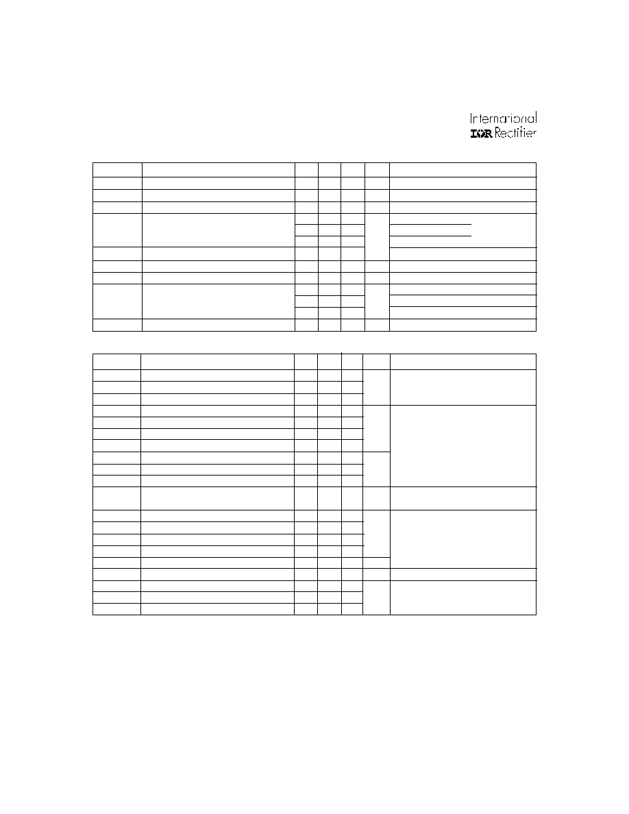
IRG4BH20K-S
2
www.irf.com
Parameter
Min. Typ. Max. Units
Conditions
Q
g
Total Gate Charge (turn-on)
--
28
43
I
C
= 5.0A
Q
ge
Gate - Emitter Charge (turn-on)
--
4.4
6.6
nC
V
CC
= 400V
See Fig.8
Q
gc
Gate - Collector Charge (turn-on)
--
12
18
V
GE
= 15V
t
d(on)
Turn-On Delay Time
--
23
--
t
r
Rise Time
--
26
--
T
J
= 25∞C
t
d(off)
Turn-Off Delay Time
--
93
140
I
C
=5.0A, V
CC
= 960V
t
f
Fall Time
--
270
400
V
GE
= 15V, R
G
= 50
E
on
Turn-On Switching Loss
--
0.45
--
Energy losses include "tail"
E
off
Turn-Off Switching Loss
--
0.44
--
mJ
See Fig. 9,10,14
E
ts
Total Switching Loss
--
0.89
1.2
t
sc
Short Circuit Withstand Time
10
--
--
µs
V
CC
=
720V, T
J
= 125∞C
V
GE
= 15V, R
G
= 50
t
d(on)
Turn-On Delay Time
--
23
--
T
J
= 150∞C,
t
r
Rise Time
--
28
--
I
C
= 5.0A, V
CC
= 960V
t
d(off)
Turn-Off Delay Time
--
100
--
V
GE
= 15V, R
G
= 50
t
f
Fall Time
--
620
--
Energy losses include "tail"
E
ts
Total Switching Loss
--
1.7
--
mJ
See Fig. 10,11,14
L
E
Internal Emitter Inductance
--
7.5
--
nH
Between lead and center of die contact
C
ies
Input Capacitance
--
435
--
V
GE
= 0V
C
oes
Output Capacitance
--
44
--
pF
V
CC
= 30V
See Fig. 7
C
res
Reverse Transfer Capacitance
--
8.3
--
= 1.0MHz
Parameter
Min. Typ. Max. Units
Conditions
V
(BR)CES
Collector-to-Emitter Breakdown Voltage
1200
--
--
V
V
GE
= 0V, I
C
= 250µA
V
(BR)ECS
Emitter-to-Collector Breakdown Voltage
18
--
--
V
V
GE
= 0V, I
C
= 1.0A
V
(BR)CES
/
T
J
Temperature Coeff. of Breakdown Voltage
--
1.13
--
V/∞C
V
GE
= 0V, I
C
= 2.5mA
--
3.17
4.3
I
C
= 5.0A V
GE
= 15V
V
CE(ON)
Collector-to-Emitter Saturation Voltage
--
4.04
--
I
C
= 11A
See Fig.2, 5
--
2.84
--
I
C
= 5.0A , T
J
= 150∞C
V
GE(th)
Gate Threshold Voltage
3.5
--
6.5
V
CE
= V
GE
, I
C
= 250µA
V
GE(th)
/
T
J
Temperature Coeff. of Threshold Voltage
--
-10
--
mV/∞C V
CE
= V
GE
, I
C
= 1mA
g
fe
Forward Transconductance
2.3
3.5
--
S
V
CE
= 100 V, I
C
= 5.0A
--
--
250
V
GE
= 0V, V
CE
= 1200V
--
--
2.0
V
GE
= 0V, V
CE
= 10V, T
J
= 25∞C
--
--
1000
V
GE
= 0V, V
CE
= 1200V, T
J
= 150∞C
I
GES
Gate-to-Emitter Leakage Current
--
--
±100
nA
V
GE
= ±20V
Electrical Characteristics @ T
J
= 25∞C (unless otherwise specified)
I
CES
Zero Gate Voltage Collector Current
V
µA
Switching Characteristics @ T
J
= 25∞C (unless otherwise specified)
ns
ns
Repetitive rating; pulse width limited by maximum
junction temperature.
Pulse width
80µs; duty factor
0.1%.
Pulse width 5.0µs, single shot.
Notes:
Repetitive rating; V
GE
= 20V, pulse width limited by
max. junction temperature. ( See fig. 13b )
V
CC
= 80%(V
CES
), V
GE
= 20V, L = 10µH, R
G
=50
,
(See fig. 13a)
* When mounted on 1" square PCB (FR-4 or G-10 Material ). For recommended footprint and soldering techniques
refer to application note #AN-994.

IRG4BH20K-S
www.irf.com
3
Fig. 1 - Typical Load Current vs. Frequency
(Load Current = I
RMS
of fundamental)
Fig. 2 - Typical Output Characteristics
Fig. 3 - Typical Transfer Characteristics
Load Current ( A )
0.1
1
10
100
1
10
V , Collector-to-Emitter Voltage (V)
I , Collector-to-Emitter Current (A)
CE
C
V = 15V
20µs PULSE WIDTH
GE
T = 150 C
J
∞
T = 25 C
J
∞
0
4
8
12
16
0.1
1
10
100
f, Frequency (kHz)
)
60% of rated
voltage
Ideal diodes
Sq u a re w a v e :
F or bot h:
Duty cycle: 50%
T = 125∞ C
T = 90∞ C
Gate drive as specified
sink
J
Tria ngu lar wave:
C la mp vol tage :
80% of rated
Po wer Di ssipation = 15W
1
10
100
6
8
10
12
14
V , Gate-to-Emitter Voltage (V)
I , Collector-to-Emitter Current (A)
GE
C
V = 50V
5µs PULSE WIDTH
CC
T = 25 C
J
∞
T = 150 C
J
∞
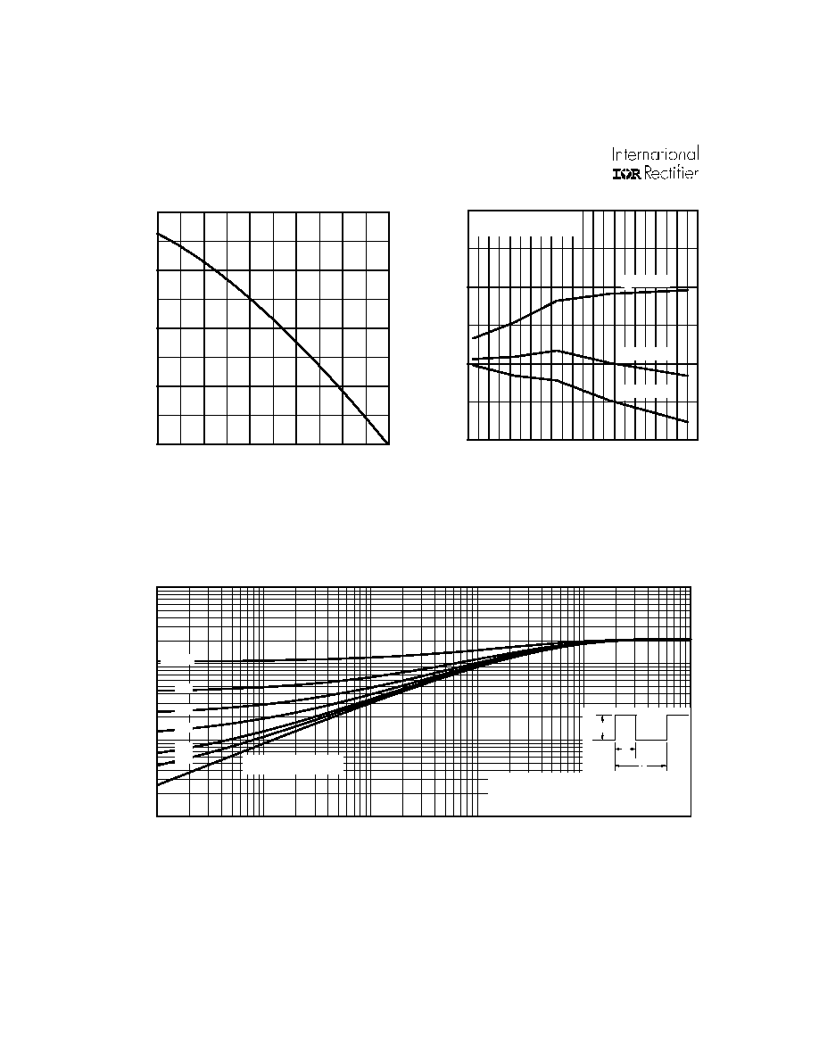
IRG4BH20K-S
4
www.irf.com
Fig. 6 - Maximum Effective Transient Thermal Impedance, Junction-to-Case
Fig. 4 - Maximum Collector Current vs. Case
Temperature
0.01
0.1
1
10
0.00001
0.0001
0.001
0.01
0.1
1
Notes:
1. Duty factor D = t / t
2. Peak T = P
x Z
+ T
1
2
J
DM
thJC
C
P
t
t
DM
1
2
t , Rectangular Pulse Duration (sec)
Thermal Response (Z )
1
thJC
0.01
0.02
0.05
0.10
0.20
D = 0.50
SINGLE PULSE
(THERMAL RESPONSE)
25
50
75
100
125
150
0
3
6
9
12
T , Case Temperature ( C)
Maximum DC Collector Current(A)
C
∞
Fig. 5 - Typical Collector-to-Emitter Voltage
vs. Junction Temperature
-60 -40 -20
0
20
40
60
80 100 120 140 160
2.0
3.0
4.0
5.0
T , Junction Temperature ( C)
V , Collector-to-Emitter Voltage(V)
J
∞
CE
V = 15V
80 us PULSE WIDTH
GE
I = A
10
C
I = A
5
C
I = A
2.5
C
T
J
, Junction Temperature ( ∞C )

IRG4BH20K-S
www.irf.com
5
Fig. 7 - Typical Capacitance vs.
Collector-to-Emitter Voltage
Fig. 8 - Typical Gate Charge vs.
Gate-to-Emitter Voltage
Fig. 9 - Typical Switching Losses vs. Gate
Resistance
1
10
100
0
200
400
600
800
V , Collector-to-Emitter Voltage (V)
C, Capacitance (pF)
CE
V
C
C
C
=
=
=
=
0V,
C
C
C
f = 1MHz
+ C
+ C
C SHORTED
GE
ies
ge
gc ,
ce
res
gc
oes
ce
gc
Cies
Coes
Cres
0
10
20
30
40
50
0.70
0.75
0.80
0.85
0.90
0.95
R , Gate Resistance (Ohm)
Total Switching Losses (mJ)
G
V = 960V
V = 15V
T = 25 C
I = 11A
CC
GE
J
C
∞
0
5
10
15
20
25
30
0
4
8
12
16
20
Q , Total Gate Charge (nC)
V , Gate-to-Emitter Voltage (V)
G
GE
V
= 400V
I
= 11A
CC
C
R
G
, Gate Resistance (
)
Fig. 10 - Typical Switching Losses vs.
Junction Temperature
-60 -40 -20
0
20
40
60
80 100 120 140 160
0.1
1
10
T , Junction Temperature ( C )
Total Switching Losses (mJ)
J
∞
R = 50Ohm
V = 15V
V = 960V
G
GE
CC
I = A
10
C
I = A
5
C
I = A
2.5
C
T
J
, Junction Temperature ( ∞C )