IRG4IBC30UD
INSULATED GATE BIPOLAR TRANSISTOR WITH
ULTRAFAST SOFT RECOVERY DIODE
Features
Features
Features
Features
Features
E
G
n-c ha nn el
C
V
CES
= 600V
V
CE(on) typ.
= 1.95V
@V
GE
= 15V, I
C
= 12A
UltraFast CoPack IGBT
7/17/2000
PD91753A
Parameter
Typ.
Max.
Units
R
JC
Junction-to-Case - IGBT
≠≠≠
2.8
R
JC
Junction-to-Case - Diode
≠≠≠
4.1
∞C/W
R
JA
Junction-to-Ambient, typical socket mount
≠≠≠
65
Wt
Weight
2.0 (0.07)
≠≠≠
g (oz)
Thermal Resistance
TO-220 FULLPAK
www.irf.com
1
Parameter
Max.
Units
V
CES
Collector-to-Emitter Voltage
600
V
I
C
@ T
C
= 25∞C
Continuous Collector Current
17
I
C
@ T
C
= 100∞C
Continuous Collector Current
8.9
I
CM
Pulsed Collector Current
Q
92
A
I
LM
Clamped Inductive Load Current
R
92
I
F
@ T
C
= 100∞C
Diode Continuous Forward Current
8.5
I
FM
Diode Maximum Forward Current
92
Visol
RMS Isolation Voltage, Terminal to Case
U
2500
V
V
GE
Gate-to-Emitter Voltage
± 20
P
D
@ T
C
= 25∞C
Maximum Power Dissipation
45
P
D
@ T
C
= 100∞C
Maximum Power Dissipation
18
T
J
Operating Junction and
-55 to +150
T
STG
Storage Temperature Range
∞C
Soldering Temperature, for 10 sec.
300 (0.063 in. (1.6mm) from case)
Mounting Torque, 6-32 or M3 Screw.
10 lbf∑in (1.1 N∑m)
Absolute Maximum Ratings
W
∑ 2.5kV, 60s insulation voltage
U
∑ 4.8 mm creapage distance to heatsink
∑ UltraFast: Optimized for high operating
frequencies 8-40 kHz in hard switching, >200
kHz in resonant mode
∑ IGBT co-packaged with HEXFRED
TM
ultrafast,
ultrasoft recovery antiparallel diodes
∑ Tighter parameter distribution
∑ Industry standard Isolated TO-220 Fullpak
TM
outline
Benefits
∑ Simplified assembly
∑ Highest efficiency and power density
∑ HEXFRED
TM
antiparallel Diode minimizes
switching losses and EMI

IRG4IBC30UD
2
www.irf.com
Parameter
Min. Typ. Max. Units
Conditions
Q
g
Total Gate Charge (turn-on)
≠≠≠
50
75
I
C
= 12A
Qge
Gate - Emitter Charge (turn-on)
≠≠≠
8.1
12
nC
V
CC
= 400V
See Fig. 8
Q
gc
Gate - Collector Charge (turn-on)
≠≠≠
18
27
V
GE
= 15V
t
d(on)
Turn-On Delay Time
≠≠≠
40
≠≠≠
T
J
= 25∞C
t
r
Rise Time
≠≠≠
21
≠≠≠
ns
I
C
= 12A, V
CC
= 480V
t
d(off)
Turn-Off Delay Time
≠≠≠
91
140
V
GE
= 15V, R
G
= 23
t
f
Fall Time
≠≠≠
80
130
Energy losses include "tail" and
E
on
Turn-On Switching Loss
≠≠≠
0.38
≠≠≠
diode reverse recovery.
E
off
Turn-Off Switching Loss
≠≠≠
0.16
≠≠≠
mJ
See Fig. 9, 10, 11, 18
E
ts
Total Switching Loss
≠≠≠
0.54
0.9
t
d(on)
Turn-On Delay Time
≠≠≠
40
≠≠≠
T
J
= 150∞C, See Fig. 9, 10, 11, 18
t
r
Rise Time
≠≠≠
22
≠≠≠
ns
I
C
= 12A, V
CC
= 480V
t
d(off)
Turn-Off Delay Time
≠≠≠
120
≠≠≠
V
GE
= 15V, R
G
= 23
t
f
Fall Time
≠≠≠
180
≠≠≠
Energy losses include "tail" and
E
ts
Total Switching Loss
≠≠≠
0.89
≠≠≠
mJ
diode reverse recovery.
L
E
Internal Emitter Inductance
≠≠≠
7.5
≠≠≠
nH
Measured 5mm from package
C
ies
Input Capacitance
≠≠≠ 1100 ≠≠≠
V
GE
= 0V
C
oes
Output Capacitance
≠≠≠
73
≠≠≠
pF
V
CC
= 30V
See Fig. 7
C
res
Reverse Transfer Capacitance
≠≠≠
14
≠≠≠
= 1.0MHz
t
rr
Diode Reverse Recovery Time
≠≠≠
42
60
ns
T
J
= 25∞C See Fig.
≠≠≠
80
120
T
J
= 125∞C 14 I
F
= 12A
I
rr
Diode Peak Reverse Recovery Current
≠≠≠
3.5
6.0
A
T
J
= 25∞C See Fig.
≠≠≠
5.6
10
T
J
= 125∞C 15 V
R
= 200V
Q
rr
Diode Reverse Recovery Charge
≠≠≠
80
180
nC
T
J
= 25∞C See Fig.
≠≠≠
220
600
T
J
= 125∞C 16 di/dt 200A/µs
di
(rec)M
/dt
Diode Peak Rate of Fall of Recovery
≠≠≠
180
≠≠≠
A/µs
T
J
= 25∞C See Fig.
During t
b
≠≠≠
120
≠≠≠
T
J
= 125∞C 17
Parameter
Min. Typ. Max. Units
Conditions
V
(BR)CES
Collector-to-Emitter Breakdown Voltage 600
≠≠≠
≠≠≠
V
V
GE
= 0V, I
C
= 250µA
V
(BR)CES
/
T
J
Temperature Coeff. of Breakdown Voltage
≠≠≠
0.63
≠≠≠
V/∞C
V
GE
= 0V, I
C
= 1.0mA
V
CE(on)
Collector-to-Emitter Saturation Voltage
≠≠≠
1.95
2.1
I
C
= 12A
V
GE
= 15V
≠≠≠
2.52
≠≠≠
V
I
C
= 23A
See Fig. 2, 5
≠≠≠
2.09
≠≠≠
I
C
= 12A, T
J
= 150∞C
V
GE(th)
Gate Threshold Voltage
3.0
≠≠≠
6.0
V
CE
= V
GE
, I
C
= 250µA
V
GE(th)
/
T
J
Temperature Coeff. of Threshold Voltage ≠≠≠
-11
≠≠≠ mV/∞C V
CE
= V
GE
, I
C
= 250µA
g
fe
Forward Transconductance
T
3.1
8.6
≠≠≠
S
V
CE
= 100V, I
C
= 12A
I
CES
Zero Gate Voltage Collector Current
≠≠≠
≠≠≠
250
µA
V
GE
= 0V, V
CE
= 600V
≠≠≠
≠≠≠ 2500
V
GE
= 0V, V
CE
= 600V, T
J
= 150∞C
V
FM
Diode Forward Voltage Drop
≠≠≠
1.4
1.7
V
I
C
= 12A
See Fig. 13
≠≠≠
1.3
1.6
I
C
= 12A, T
J
= 150∞C
I
GES
Gate-to-Emitter Leakage Current
≠≠≠
≠≠≠ ±100
nA
V
GE
= ±20V
Switching Characteristics @ T
J
= 25∞C (unless otherwise specified)
Electrical Characteristics @ T
J
= 25∞C (unless otherwise specified)
IRG4IBC30UD
www.irf.com
3
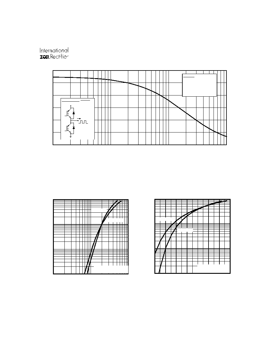
Fig. 1 - Typical Load Current vs. Frequency
(Load Current = I
RMS
of fundamental)
Fig. 2 - Typical Output Characteristics
Fig. 3 - Typical Transfer Characteristics
0 . 1
1
1 0
1 0 0
0 . 1
1
1 0
C E
C
I
,
C
o
l
l
e
c
t
or
-
t
o-
E
m
i
t
t
e
r
C
u
r
r
ent
(
A
)
V , C o lle cto r-to -E m itte r V o lta g e (V )
T = 1 5 0 ∞C
T = 2 5 ∞ C
J
J
V = 1 5 V
2 0 µ s P U L S E W ID T H
G E
A
0 . 1
1
1 0
1 0 0
5
6
7
8
9
1 0
1 1
1 2
C
I
,
C
o
l
l
e
c
to
r
-
to
-
E
m
i
tt
e
r
C
u
r
r
e
n
t
(
A
)
G E
T = 2 5 ∞C
T = 1 5 0 ∞C
J
J
V , G a te -to -E m itte r V o lta g e (V )
A
V = 1 0 V
5 µ s P U L S E W ID T H
C C
0.1
1
10
100
0
2
4
6
8
10
12
f, Frequency (KHz)
LOAD CURRENT (A)
F o r b o th :
D u ty c y c le : 5 0 %
T = 1 2 5 ∞ C
T = 9 0 ∞ C
G a te d riv e a s s p e c ifi e d
sink
J
P o w e r D is s ip a tio n = W
6 0% of rate d
volta ge
I
Id e a l d io d e s
S q u a re w a v e :
13

IRG4IBC30UD
4
www.irf.com
Fig. 5 - Typical Collector-to-Emitter Voltage
vs. Junction Temperature
Fig. 4 - Maximum Collector Current vs.
Case Temperature
Fig. 6 - Maximum IGBT Effective Transient Thermal Impedance, Junction-to-Case
1 . 5
2 . 0
2 . 5
3 . 0
- 6 0
- 4 0
- 2 0
0
2 0
4 0
6 0
8 0
1 0 0
1 2 0
1 4 0
1 6 0
CE
V
,
C
o
lle
c
t
o
r
-
t
o
-
E
m
it
t
e
r
V
o
lt
a
g
e
(
V
)
V = 1 5 V
8 0 µ s P U L S E W ID T H
G E
A
T , Ju n c tio n T e m p e ra tu re (∞C )
J
I = 2 4 A
I = 1 2 A
I = 6 .0 A
C
C
C
0.01
0.1
1
10
0.00001
0.0001
0.001
0.01
0.1
1
10
Notes:
1. Duty factor D = t / t
2. Peak T = P
x Z
+ T
1
2
J
DM
thJC
C
P
t
t
DM
1
2
t , Rectangular Pulse Duration (sec)
Thermal Response (Z )
1
thJC
0.01
0.02
0.05
0.10
0.20
D = 0.50
SINGLE PULSE
(THERMAL RESPONSE)
25
50
75
100
125
150
0
4
8
12
16
20
T , Case Temperature ( C)
Maximum DC Collector Current(A)
C
∞

IRG4IBC30UD
www.irf.com
5
Fig. 7 - Typical Capacitance vs.
Collector-to-Emitter Voltage
Fig. 8 - Typical Gate Charge vs.
Gate-to-Emitter Voltage
Fig. 9 - Typical Switching Losses vs. Gate
Resistance
Fig. 10 - Typical Switching Losses vs.
Junction Temperature
0
4 0 0
8 0 0
1 2 0 0
1 6 0 0
2 0 0 0
1
1 0
1 0 0
C E
C
,
C
apa
ci
t
a
nc
e
(
p
F
)
V , C o lle c to r-to -E m itte r V o lta g e (V )
A
V = 0V , f = 1 M H z
C = C + C , C S H O R TE D
C = C
C = C + C
G E
ie s g e g c ce
re s gc
o e s ce g c
C
ie s
C
re s
C
o e s
0
4
8
1 2
1 6
2 0
0
1 0
2 0
3 0
4 0
5 0
GE
V
, G
a
te
-
t
o
-
E
m
i
t
te
r
V
o
l
t
a
g
e
(
V
)
g
Q , T o ta l G a te C h a rg e (n C )
A
V = 4 0 0 V
I = 1 2 A
C E
C
Total Switchig Losses (mJ)
0 . 1
1
1 0
- 6 0
- 4 0
- 2 0
0
2 0
4 0
6 0
8 0
1 0 0
1 2 0
1 4 0
1 6 0
A
T , Junction Tem perature (∞C)
J
R = 23
V = 15V
V = 480V
I = 24A
I = 12A
I = 6.0A
G
G E
C C
C
C
C
Total Switchig Losses (mJ)
0 . 5 0
0 . 5 2
0 . 5 4
0 . 5 6
0 . 5 8
0 . 6 0
0
1 0
2 0
3 0
4 0
5 0
6 0
G
A
R , G ate Resistance (
)
V = 480V
V = 15V
T = 25∞C
I = 12A
C C
G E
J
C