C-101
Revision 1
IRGBC30FD2
INSULATED GATE BIPOLAR TRANSISTOR
WITH ULTRAFAST SOFT RECOVERY
DIODE
Features
∑ Switching-loss rating includes all "tail" losses
∑ HEXFRED
TM
soft ultrafast diodes
∑ Optimized for medium operating frequency (1 to
10kHz) See Fig. 1 for Current vs. Frequency curve
E
G
n-channel
C
V
CES
= 600V
V
CE(sat)
2.1V
@V
GE
= 15V, I
C
= 31A
Parameter
Min.
Typ.
Max.
Units
R
JC
Junction-to-Case - IGBT
--
--
1.2
R
JC
Junction-to-Case - Diode
--
--
2.5
∞C/W
R
CS
Case-to-Sink, flat, greased surface
--
0.50
--
R
JA
Junction-to-Ambient, typical socket mount
--
--
80
Wt
Weight
--
2 (0.07)
--
g (oz)
Thermal Resistance
Absolute Maximum Ratings
Description
Co-packaged IGBTs are a natural extension of International Rectifier's well
known IGBT line. They provide the convenience of an IGBT and an ultrafast
recovery diode in one package, resulting in substantial benefits to a host of
high-voltage, high-current, motor control, UPS and power supply applications.
Fast CoPack IGBT
PD - 9.794
TO-220AB
Parameter
Max.
Units
V
CES
Collector-to-Emitter Voltage
600
V
I
C
@ T
C
= 25∞C
Continuous Collector Current
31
I
C
@ T
C
= 100∞C
Continuous Collector Current
17
I
CM
Pulsed Collector Current
120
A
I
LM
Clamped Inductive Load Current
120
I
F
@ T
C
= 100∞C
Diode Continuous Forward Current
12
I
FM
Diode Maximum Forward Current
120
V
GE
Gate-to-Emitter Voltage
± 20
V
P
D
@ T
C
= 25∞C
Maximum Power Dissipation
100
W
P
D
@ T
C
= 100∞C
Maximum Power Dissipation
42
T
J
Operating Junction and
-55 to +150
T
STG
Storage Temperature Range
∞C
Soldering Temperature, for 10 sec.
300 (0.063 in. (1.6mm) from case)
Mounting Torque, 6-32 or M3 Screw.
10 lbf∑in (1.1 N∑m)
Next Data Sheet
Index
Previous Datasheet
To Order
C-102
Parameter
Min. Typ. Max. Units
Conditions
Q
g
Total Gate Charge (turn-on)
--
27
30
I
C
= 17A
Q
ge
Gate - Emitter Charge (turn-on)
--
4.1
5.9
nC
V
CC
= 400V
Q
gc
Gate - Collector Charge (turn-on)
--
12
15
See Fig. 8
t
d(on)
Turn-On Delay Time
--
72
--
T
J
= 25∞C
t
r
Rise Time
--
75
--
ns
I
C
= 17A, V
CC
= 480V
t
d(off)
Turn-Off Delay Time
--
300
450
V
GE
= 15V, R
G
= 23
t
f
Fall Time
--
220
350
Energy losses include "tail" and
E
on
Turn-On Switching Loss
--
0.9
--
diode reverse recovery.
E
off
Turn-Off Switching Loss
--
2.1
--
mJ
See Fig. 9, 10, 11, 18
E
ts
Total Switching Loss
--
3.0
4.6
t
d(on)
Turn-On Delay Time
--
70
--
T
J
= 150∞C, See Fig. 9, 10, 11, 18
t
r
Rise Time
--
75
--
ns
I
C
= 17A, V
CC
= 480V
t
d(off)
Turn-Off Delay Time
--
420
--
V
GE
= 15V, R
G
= 23
t
f
Fall Time
--
480
--
Energy losses include "tail" and
E
ts
Total Switching Loss
--
4.7
--
mJ
diode reverse recovery.
L
E
Internal Emitter Inductance
--
7.5
--
nH
Measured 5mm from package
C
ies
Input Capacitance
--
660
--
V
GE
= 0V
C
oes
Output Capacitance
--
100
--
pF
V
CC
= 30V
See Fig. 7
C
res
Reverse Transfer Capacitance
--
10
--
= 1.0MHz
t
rr
Diode Reverse Recovery Time
--
42
60
ns
T
J
= 25∞C See Fig.
--
80
120
T
J
= 125∞C 14 I
F
= 12A
I
rr
Diode Peak Reverse Recovery Current
--
3.5
6.0
A
T
J
= 25∞C See Fig.
--
5.6
10
T
J
= 125∞C 15 V
R
= 200V
Q
rr
Diode Reverse Recovery Charge
--
80
180
nC
T
J
= 25∞C See Fig.
--
220
600
T
J
= 125∞C 16 di/dt = 200A/µs
di
(rec)M
/dt
Diode Peak Rate of Fall of Recovery
--
180
--
A/µs
T
J
= 25∞C See Fig.
During t
b
--
120
--
T
J
= 125∞C 17
Parameter
Min. Typ. Max. Units
Conditions
V
(BR)CES
Collector-to-Emitter Breakdown Voltage
600
--
--
V
V
GE
= 0V, I
C
= 250µA
V
(BR)CES
/
T
J
Temp. Coeff. of Breakdown Voltage
--
0.69
--
V/∞C
V
GE
= 0V, I
C
= 1.0mA
V
CE(on)
Collector-to-Emitter Saturation Voltage
--
1.8
2.1
I
C
= 17A
V
GE
= 15V
--
2.4
--
V
I
C
= 31A
See Fig. 2, 5
--
2.2
--
I
C
= 17A, T
J
= 150∞C
V
GE(th)
Gate Threshold Voltage
3.0
--
5.5
V
CE
= V
GE
, I
C
= 250µA
V
GE(th)
/
T
J
Temp. Coeff. of Threshold Voltage
--
-11
-- mV/∞C V
CE
= V
GE
, I
C
= 250µA
g
fe
Forward Transconductance
6.1
10
--
S
V
CE
= 100V, I
C
= 17A
I
CES
Zero Gate Voltage Collector Current
--
--
250
µA
V
GE
= 0V, V
CE
= 600V
--
--
2500
V
GE
= 0V, V
CE
= 600V, T
J
= 150∞C
V
FM
Diode Forward Voltage Drop
--
1.4
1.7
V
I
C
= 12A
See Fig. 13
--
1.3
1.6
I
C
= 12A, T
J
= 150∞C
I
GES
Gate-to-Emitter Leakage Current
--
--
±100
nA
V
GE
= ±20V
IRGBC30FD2
Pulse width
80µs; duty factor
0.1%.
V
CC
=80%(V
CES
), V
GE
=20V, L=10µH,
R
G
= 23
, ( See fig. 19 )
Pulse width 5.0µs,
single shot.
Switching Characteristics @ T
J
= 25∞C (unless otherwise specified)
Electrical Characteristics @ T
J
= 25∞C (unless otherwise specified)
Repetitive rating; V
GE
=20V, pulse width
limited by max. junction temperature.
( See fig. 20 )
Notes:
Next Data Sheet
Index
Previous Datasheet
To Order
C-103
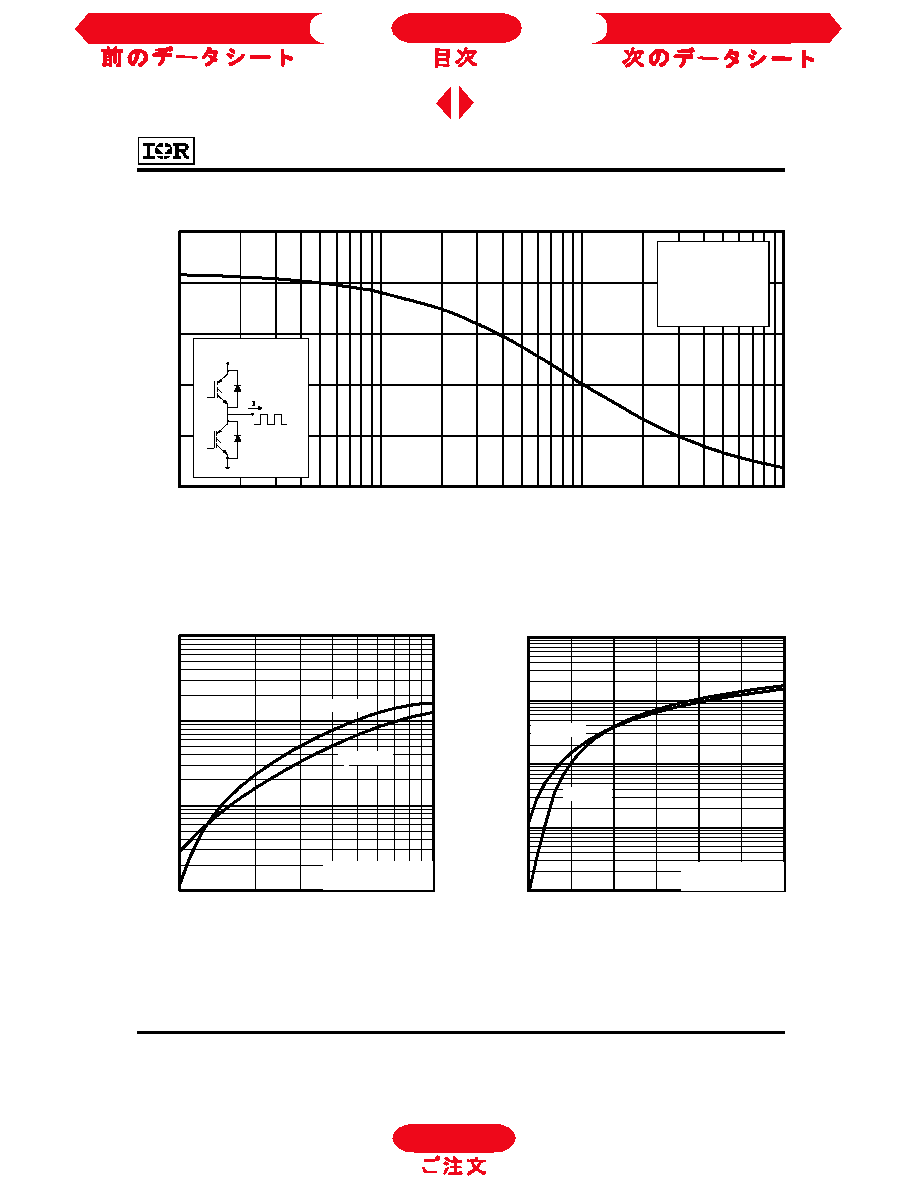
Fig. 1 - Typical Load Current vs. Frequency
(Load Current = I
RMS
of fundamental)
Fig. 2 - Typical Output Characteristics
Fig. 3 - Typical Transfer Characteristics
IRGBC30FD2
0
4
8
12
16
20
0.1
1
10
100
f, Frequency (kHz)
L
o
a
d
C
u
r
r
e
n
t
(
A
)
A
6 0 % o f ra te d
v o lta g e
Du ty c ycl e: 5 0 %
T = 1 2 5 ∞C
T = 9 0 ∞C
Ga te d rive as sp e cified
Tu rn -on lo sses in clud e
effe cts o f re verse rec ove ry
s in k
J
P o we r D issipatio n = 2 1W
1
1 0
1 0 0
1 0 0 0
1
1 0
C E
C
I
,
C
o
l
l
e
c
t
o
r
-
t
o
-
E
m
i
t
t
e
r
C
u
r
r
e
n
t
(
A
)
V , C ollector-to-E m itter V oltage (V )
T = 15 0∞C
T = 25 ∞C
J
J
V = 1 5V
2 0µ s P U LS E W ID T H
G E
0 .1
1
1 0
1 0 0
1 0 0 0
5
1 0
1 5
2 0
C
I
,
C
o
l
l
e
c
t
o
r
-
t
o
-
E
m
i
t
t
e
r
C
u
r
r
e
n
t
(
A
)
V , G a te -to -E m itte r V o lta g e (V )
G E
T = 25 ∞C
T = 15 0∞C
J
J
V = 1 00 V
5 µs P U L S E W ID T H
C C
To Order
Next Data Sheet
Index
Previous Datasheet

C-104
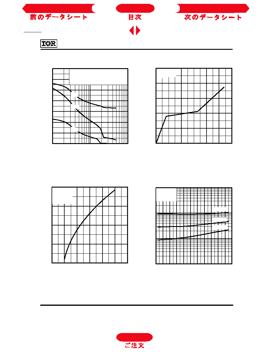
Fig. 5 - Collector-to-Emitter Voltage vs.
Case Temperature
Fig. 4 - Maximum Collector Current vs.
Case Temperature
IRGBC30FD2
Fig. 6 - Maximum IGBT Effective Transient Thermal Impedance, Junction-to-Case
1 .0
1 .5
2 .0
2 .5
3 .0
3 .5
-6 0
-4 0
-2 0
0
2 0
4 0
6 0
8 0
1 0 0 1 2 0 1 4 0 1 6 0
T , C ase T em perature (∞C )
C
C
E
V
,
C
o
l
l
e
c
t
o
r
-
t
o
-
E
m
i
t
t
e
r
V
o
l
t
a
g
e
(
V
)
V = 1 5 V
80 µs P U L S E W ID T H
G E
I = 34 A
I = 17 A
I = 8.5A
C
C
C
0
1 0
2 0
3 0
4 0
2 5
5 0
7 5
1 0 0
1 2 5
1 5 0
M
a
x
i
m
u
m
D
C
C
o
l
l
e
c
t
o
r
C
u
r
r
e
n
t
(
A
)
T , C a s e T e m p e ra tu re (∞C )
C
V = 15 V
G E
0 .0 1
0 .1
1
1 0
0 .0 0 0 0 1
0 .0 0 0 1
0 .0 0 1
0 .0 1
0 .1
1
1 0
t , R e c ta n gu la r P u ls e D ura tio n (s e c )
1
t
h
J
C
D = 0 .5 0
0 .0 1
0 .0 2
0 .0 5
0 .1 0
0 .2 0
S IN G L E P U L S E
(T H E R M A L R E S P O N S E )
T
h
e
r
m
a
l
R
e
s
p
o
n
s
e
(
Z
)
P
t
2
1
t
D M
N o te s :
1 . D u ty fa c to r D = t / t
2 . P e a k T = P x Z + T
1
2
J
D M
th J C
C
To Order
Next Data Sheet
Index
Previous Datasheet
C-105
IRGBC30FD2
Fig. 7 - Typical Capacitance vs.
Collector-to-Emitter Voltage
Fig. 8 - Typical Gate Charge vs.
Gate-to-Emitter Voltage
Fig. 9 - Typical Switching Losses vs. Gate
Resistance
Fig. 10 - Typical Switching Losses vs.
Case Temperature
2.94
2.98
3.02
3.06
3.10
0
10
20
30
40
50
60
G
T
o
t
a
l
S
w
i
t
c
h
i
n
g
L
o
s
s
e
s
(
m
J
)
R , Gate Resistance (
)
A
V = 480V
V = 15V
T = 25∞C
I = 17A
CC
GE
C
C
0.1
1
10
100
-60 -40 -20
0
20
40
60
80
100 120 140 160
C
T , Case Temperature (∞C)
T
o
t
a
l
S
w
i
t
c
h
i
n
g
L
o
s
s
e
s
(
m
J
)
A
R = 23
V = 15V
V = 480V
G
GE
CC
I = 17A
I = 34A
I = 8.5A
C
C
C
0
2 00
4 00
6 00
8 00
1 0 00
1 2 00
1 4 00
1
1 0
10 0
C E
C
,
C
a
p
a
c
i
t
a
n
c
e
(
p
F
)
V , C o lle c to r-to -E m itte r V o lta g e (V )
V = 0V, f = 1MHz
C = C + C , C SHORTED
C = C
C = C + C
GE
ies ge gc ce
res gc
oes ce gc
C
ies
C
res
C
oes
0
4
8
12
16
20
0
5
1 0
1 5
20
2 5
3 0
G
E
V
,
G
a
t
e
-
t
o
-
E
m
i
t
t
e
r
V
o
l
t
a
g
e
(
V
)
Q , T otal G ate C harge (nC )
g
V = 40 0 V
I = 1 7A
C E
C
To Order
Next Data Sheet
Index
Previous Datasheet