IRGMC40F.p65
IRGMC40F
INSULATED GATE BIPOLAR TRANSISTOR
E
C
G
n-channel
Features
V
CES
= 600V
V
CE(on) max
= 2.0V
@V
GE
= 15V, I
C
= 20A
Parameter
Max.
Units
V
CES
Collector-to-Emitter Breakdown Voltage
600
V
I
C
@ T
C
= 25�C
Continuous Collector Current
35*
I
C
@ T
C
= 100�C
Continuous Collector Current
20
A
I
CM
Pulsed Collector Current
152
I
LM
Clamped Inductive Load Current
152
V
GE
Gate-to-Emitter Voltage
� 20
V
P
D
@ T
C
= 25�C
Maximum Power Dissipation
125
W
P
D
@ T
C
= 100�C
Maximum Power Dissipation
50
T
J
Operating Junction and
-55 to + 150
T
STG
Storage Temperature Range
�C
Lead Temperature
300 (0.063in./1.6mm from case for 10s)
Weight
9.3 (typical)
g
Absolute Maximum Ratings
02/20/02
www.irf.com
1
Fast Speed IGBT
� Electrically Isolated and Hermetically Sealed
� Simple Drive Requirements
� Latch-proof
� Fast Speed operation 3 kHz - 8 kHz
� Switching-loss rating includes all "tail" losses
Insulated Gate Bipolar Transistors (IGBTs) from International Rectifier have
higher usable current densities than comparable bipolar transistors, while at the
same time having simpler gate-drive requirements of the familiar power MOSFET.
They provide substantial benefits to a host of high-voltage, high-current
applications.
TO-254AA
Thermal Resistance
Parameter
Min Typ Max
Units
Test Conditions
RthJC
Junction-to-Case
--
--
1.0
RthCS
Case-to-Sink
--
0.21
--
RthJA
Junction-to-Ambient
--
--
48
�C/W
PD -90716B
The performance of various IGBTs varies greatly with frequency. Note that IR now
provides the designer with a speed benchmark (f
Ic/2
, or the "half-current frequency "),
as well as an indication of the current handling capability of the device.
Description
*
Current is limited by pin diameter
For footnotes refer to the last page
2
www.irf.com
IRGMC40F
Parameter
Min. Typ. Max. Units
Conditions
Q
g
Total Gate Charge (turn-on)
���
58
116
I
C
= 20A
Q
ge
Gate - Emitter Charge (turn-on)
���
8.0
16
nC
V
CC
= 300V
See Fig. 8
Q
gc
Gate - Collector Charge (turn-on)
���
30
60
V
GE
= 15V
t
d(on)
Turn-On Delay Time
���
���
52
I
C
= 20A, V
CC
= 480V
t
r
Rise Time
���
���
74
V
GE
= 15V, R
G
= 9.1
t
d(off)
Turn-Off Delay Time
���
���
410
Energy losses include "tail"
t
f
Fall Time
���
���
420
See Fig. 9, 10 & 13
E
on
Turn-On Switching Loss
���
0.6
���
E
off
Turn-off Switching Loss
���
3.8
���
E
ts
Total Switching Loss
���
4.4
9.0
t
d(on)
Turn-On Delay Time
���
28
���
T
J
= 125�C
t
r
Rise Time
���
37
���
I
C
= 20A, V
CC
= 480V
t
d(off)
Turn-Off Delay Time
���
380
���
V
GE
= 15V, R
G
= 9.1
t
f
Fall Time
���
460
���
Energy losses include "tail"
E
ts
Total Switching Loss
���
7.0
���
See Fig. 11, 13
L
C
+L
E
Total Inductance
���
6.8
���
nH
Measured from Collector lead (6mm/
0.25in. from package) to Emitter
lead (6mm / 0.25in. from package)
C
ies
Input Capacitance
��� 1500 ���
V
GE
= 0V
C
oes
Output Capacitance
���
190
���
pF
V
CC
= 30V
See Fig. 7
C
res
Reverse Transfer Capacitance
���
20
���
= 1.0MHz
C
res
Reverse Transfer Capacitance
���
12
���
Parameter
Min. Typ. Max. Units
Conditions
V
(BR)CES
Collector-to-Emitter Breakdown Voltage
600
���
���
V
V
GE
= 0V, I
C
= 1.0 mA
V
(BR)ECS
Emitter-to-Collector Breakdown Voltage
24
���
���
V
V
GE
= 0V, I
C
= 1.0 A
V
(BR)CES
/
T
J
Temperature Coeff. of Breakdown Voltage
���
0.7
���
V/�C
V
GE
= 0V, I
C
= 1.0 mA
���
���
2.0
I
C
= 20A V
GE
= 15V
V
CE(ON)
Collector-to-Emitter Saturation Voltage
���
2.2
���
I
C
= 35A See Fig.5
���
1.9
���
I
C
= 20A , T
J
= 125�C
V
GE(th)
Gate Threshold Voltage
3.0
���
5.5
V
CE
= V
GE
, I
C
= 250 �A
V
GE(th)
/
T
J
Temperature Coeff. of Threshold Voltage
���
-12
���
mV/�C V
CE
= V
GE
, I
C
= 250 �A
g
fe
Forward Transconductance
T
9.2
���
���
S
V
CE
15V, I
C
= 20A
���
���
50
V
GE
= 0V, V
CE
= 480V
���
���
1000
V
GE
= 0V, V
CE
= 480V, T
J
= 125�C
I
GES
Gate-to-Emitter Leakage Current
���
���
�100
nA
V
GE
= �20V
Electrical Characteristics @ T
J
= 25�C (unless otherwise specified)
I
CES
Zero Gate Voltage Collector Current
� A
Switching Characteristics @ T
J
= 25�C (unless otherwise specified)
V
ns
mJ
ns
mJ
For footnotes refer to the last page
Note: Corresponding Spice and Saber models are available on the Website.
www.irf.com
3
IRGMC40F
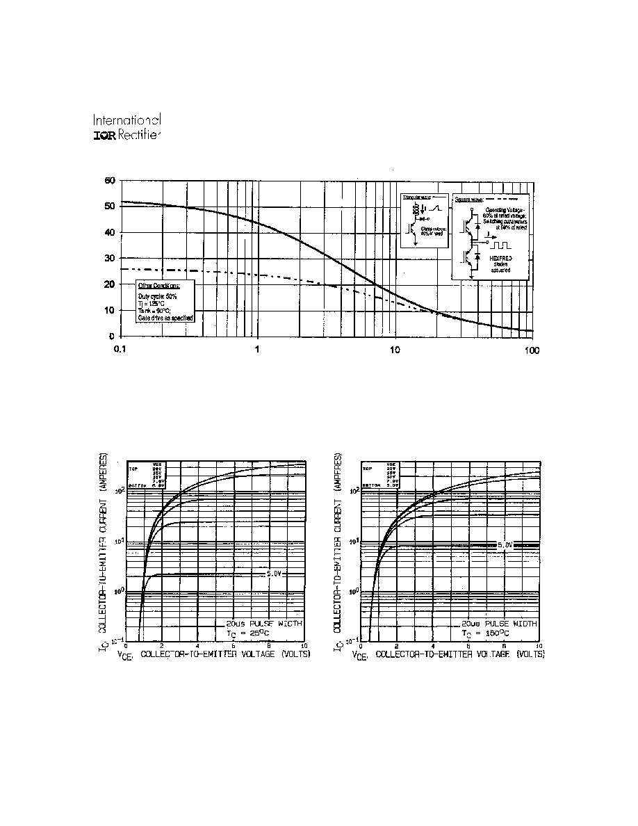
Fig. 1 - Typical Load Current vs. Frequency
(For square wave, I=I
RMS
of fundamental; for triangular wave, I=I
PK
)
Fig. 2 - Typical Output Characteristics
Fig. 3 - Typical Transfer Characteristics
4
www.irf.com
IRGMC40F
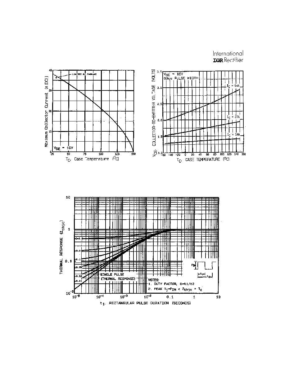
Fig. 6 - Maximum Effective Transient Thermal Impedance, Junction-to-Case
Fig. 5 - Collector-to-Emitter Voltage vs.
Junction Temperature
Fig. 4 - Maximum Collector Current vs. Case
Temperature
www.irf.com
5
IRGMC40F
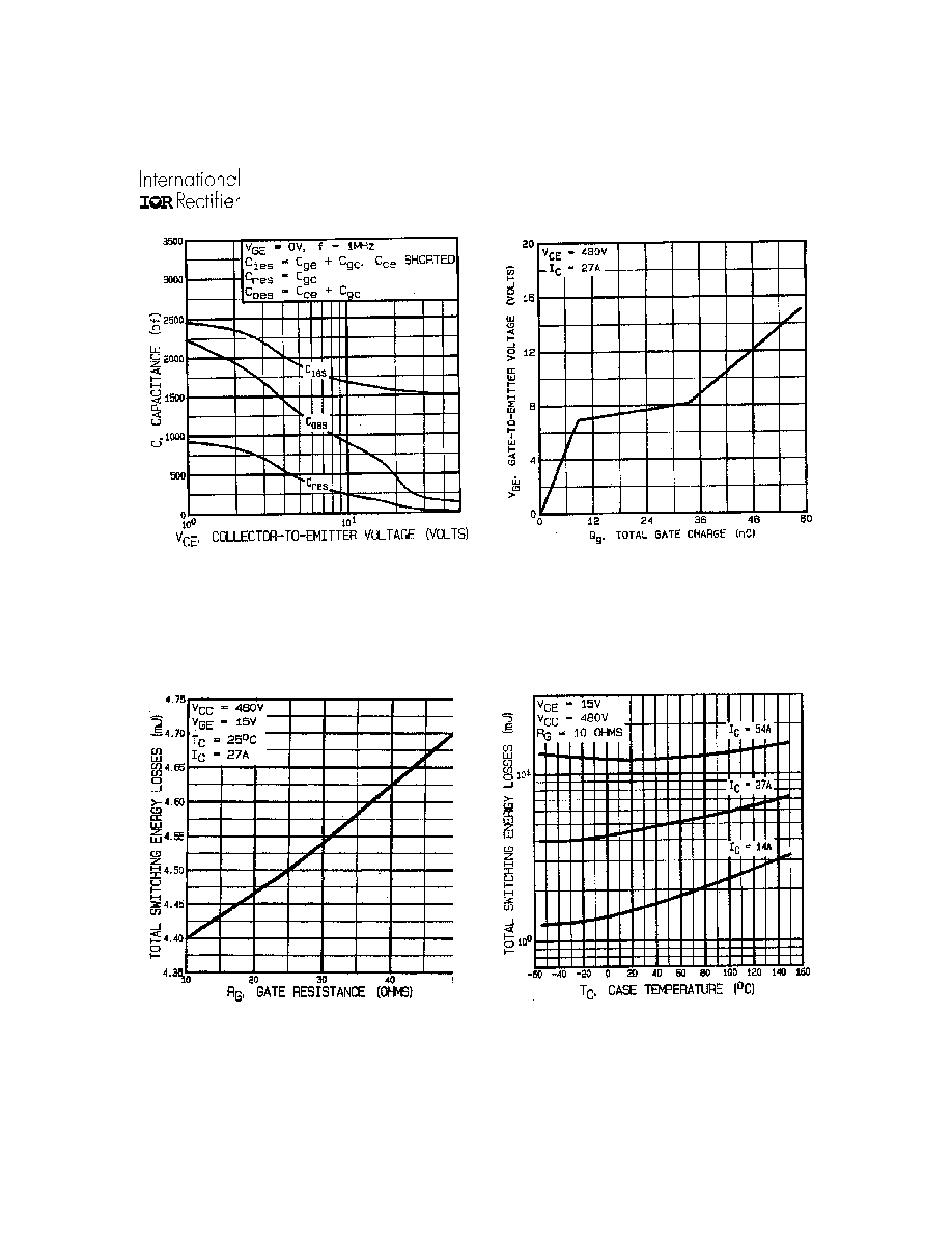
Fig. 10 - Typical Switching Losses vs.
Junction Temperature
Fig. 9 - Typical Switching Losses vs. Gate
Resistance
Fig. 8 - Typical Gate Charge vs.
Gate-to-Emitter Voltage
Fig. 7 - Typical Capacitance vs.
Collector-to-Emitter Voltage