 | –≠–ª–µ–∫—Ç—Ä–æ–Ω–Ω—ã–π –∫–æ–º–ø–æ–Ω–µ–Ω—Ç: IRGPC20K | –°–∫–∞—á–∞—Ç—å:  PDF PDF  ZIP ZIP |

IRGPC20K
Short Circuit Rated
UltraFast IGBT
INSULATED GATE BIPOLAR TRANSISTOR
Parameter
Min.
Typ.
Max.
Units
R
JC
Junction-to-Case
--
--
2.1
R
CS
Case-to-Sink, flat, greased surface
--
0.24
--
∞C/W
R
JA
Junction-to-Ambient, typical socket mount
--
--
40
Wt
Weight
--
6 (0.21)
--
g (oz)
Features
∑ Short circuit rated - 10µs @ 125∞C, V
GE
= 15V
∑ Switching-loss rating includes all "tail" losses
∑ Optimized for high operating frequency (over
5kHz)
See Fig. 1 for Current vs. Frequency
curve
V
CES
= 600V
V
CE(sat)
3.5V
@V
GE
= 15V, I
C
= 6.0A
E
C
G
n-channel
Absolute Maximum Ratings
Parameter
Max.
Units
V
CES
Collector-to-Emitter Voltage
600
V
I
C
@ T
C
= 25∞C
Continuous Collector Current
10
I
C
@ T
C
= 100∞C
Continuous Collector Current
6.0
A
I
CM
Pulsed Collector Current
20
I
LM
Clamped Inductive Load Current
20
t
sc
Short Circuit Withstand Time
10
µs
V
GE
Gate-to-Emitter Voltage
±20
V
E
ARV
Reverse Voltage Avalanche Energy
5.0
mJ
P
D
@ T
C
= 25∞C
Maximum Power Dissipation
60
W
P
D
@ T
C
= 100∞C
Maximum Power Dissipation
24
T
J
Operating Junction and
-55 to +150
T
STG
Storage Temperature Range
∞C
Soldering Temperature, for 10 sec.
300 (0.063 in. (1.6mm) from case)
Mounting torque, 6-32 or M3 screw.
10 lbf∑in (1.1N∑m)
TO -2 4 7 AC
PD - 9.1129
Thermal Resistance
Insulated Gate Bipolar Transistors (IGBTs) from International Rectifier
have higher usable current densities than comparable bipolar transistors,
while at the same time having simpler gate-drive requirements of the
familiar power MOSFET. They provide substantial benefits to a host of
high-voltage, high-current applications.
These new short circuit rated devices are especially suited for motor
control and other applications requiring short circuit withstand capability.
Description
IRGPC20K
N o t e s :
V
CC
=80%(V
CES
), V
GE
=20V, L=10µH,
R
G
= 50
, ( See fig. 13a )
Repetitive rating; V
GE
=20V, pulse width
limited by max. junction temperature.
( See fig. 13b )
Repetitive rating; pulse width limited
by maximum juntion temperature.
Pulse width
80µs; duty factor
0.1%.
Pulse width 5.0µs,
single shot.
Switching Characteristics @ T
J
= 25∞C (unless otherwise specified)
Parameter
Min. Typ. Max. Units
Conditions
Q
g
Total Gate Charge (turn-on)
--
17
26
I
C
= 6.0A
Q
ge
Gate - Emitter Charge (turn-on)
--
4.3
6.8
nC
V
CC
= 400V
See Fig. 8
Q
gc
Gate - Collector Charge (turn-on)
--
6.4
11
V
GE
= 15V
t
d(on)
Turn-On Delay Time
--
29
--
T
J
= 25∞C
t
r
Rise Time
--
18
--
ns
I
C
= 6.0A, V
CC
= 480V
t
d(off)
Turn-Off Delay Time
--
58
90
V
GE
= 15V, R
G
= 50
t
f
Fall Time
--
120
200
Energy losses include "tail"
E
on
Turn-On Switching Loss
--
0.11
--
E
off
Turn-Off Switching Loss
--
0.13
--
mJ
See Fig. 9, 10, 11, 14
E
ts
Total Switching Loss
--
0.24 0.31
t
sc
Short Circuit Withstand Time
10
--
--
µs
V
CC
= 400V, T
J
= 125∞C
V
GE
= 15V, R
G
= 50
, V
CPK
< 500V
t
d(on)
Turn-On Delay Time
--
28
--
T
J
= 150∞C,
t
r
Rise Time
--
22
--
ns
I
C
= 6.0A, V
CC
= 480V
t
d(off)
Turn-Off Delay Time
--
200
--
V
GE
= 15V, R
G
= 50
t
f
Fall Time
--
145
--
Energy losses include "tail"
E
ts
Total Switching Loss
--
0.50
--
mJ
See Fig. 10, 14
L
E
Internal Emitter Inductance
--
13
--
nH
Measured 5mm from package
C
ies
Input Capacitance
--
360
--
V
GE
= 0V
C
oes
Output Capacitance
--
45
--
pF
V
CC
= 30V
See Fig. 7
C
res
Reverse Transfer Capacitance
--
4.7
--
= 1.0MHz
Parameter
Min. Typ. Max. Units
Conditions
V
(BR)CES
Collector-to-Emitter Breakdown Voltage
600
--
--
V
V
GE
= 0V, I
C
= 250µA
V
(BR)ECS
Emitter-to-Collector Breakdown Voltage
20
--
--
V
V
GE
= 0V, I
C
= 1.0A
V
(BR)CES
/
T
J
Temperature Coeff. of Breakdown Voltage--
0.37
--
V/∞C
V
GE
= 0V, I
C
= 1.0mA
V
CE(on)
Collector-to-Emitter Saturation Voltage
--
2.4
3.5
I
C
= 6.0A
V
GE
= 15V
--
3.6
--
V
I
C
= 10A
See Fig. 2, 5
--
2.9
--
I
C
= 6.0A, T
J
= 150∞C
V
GE(th)
Gate Threshold Voltage
3.0
--
5.5
V
CE
= V
GE
, I
C
= 250µA
V
GE(th)
/
T
J
Temperature Coeff. of Threshold Voltage --
-11
--
mV/∞C V
CE
= V
GE
, I
C
= 250µA
g
fe
Forward Transconductance
1.9
3.3
--
S
V
CE
= 100V, I
C
= 6.0A
I
CES
Zero Gate Voltage Collector Current
--
--
250
µA
V
GE
= 0V, V
CE
= 600V
--
--
1000
V
GE
= 0V, V
CE
= 600V, T
J
= 150∞C
I
GES
Gate-to-Emitter Leakage Current
--
--
±100
nA
V
GE
= ±20V
Electrical Characteristics @ T
J
= 25∞C (unless otherwise specified)
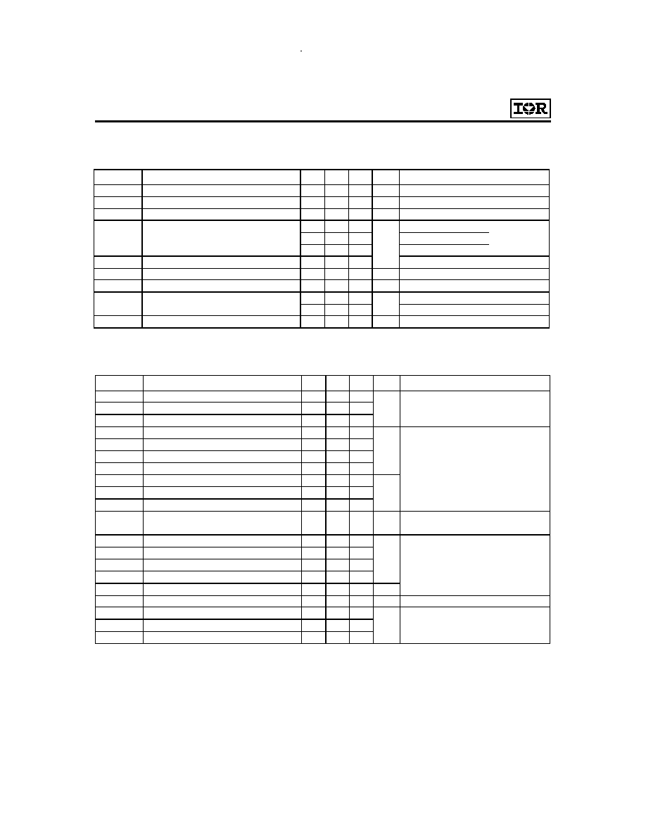
Fig. 1 - Typical Load Current vs. Frequency
(For square wave, I=I
RMS
of fundamental; for triangular wave, I=I
PK
)
Fig. 2 - Typical Output Characteristics
Fig. 3 - Typical Transfer Characteristics
IRGPC20K
0
4
8
12
16
0.1
1
10
100
f, Frequency (kHz)
Loa
d Cu
rren
t (A
)
60% of rated
voltage
Ideal diodes
Square wave:
Triangular wave:
Clamp voltage:
80% of rated
For both:
Duty cycle: 50%
T = 125∞C
T = 90∞C
Gate drive as specified
sink
J
Power Dissipation = 15W
A
0.1
1
10
100
0.1
1
10
CE
C
I
, Colle
ctor-to-Emitte
r Current
(A)
V , Collector-to-Emitter Voltage (V)
T = 150∞C
T = 25∞C
J
J
V = 15V
20µs PULSE WIDTH
GE
1
10
100
5
10
15
20
C
I
,
Co
lle
c
t
o
r
-
t
o
-
E
m
it
t
e
r
Cu
r
r
e
n
t
(
A
)
V , Gate-to-Emitter Voltage (V)
GE
T = 25∞C
T = 150∞C
J
J
V = 100V
5µs PULSE WIDTH
CC
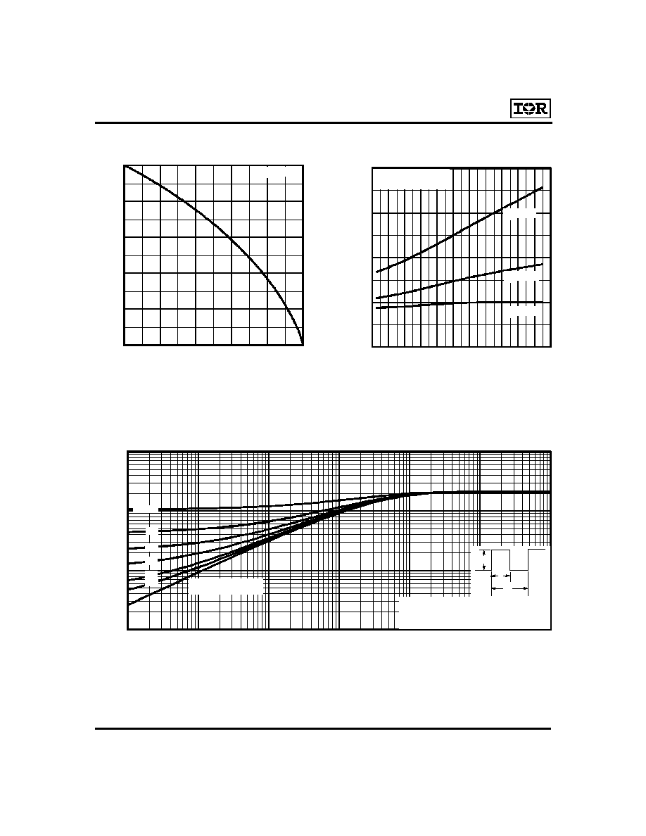
Fig. 5 - Collector-to-Emitter Voltage vs.
Case Temperature
Fig. 4 - Maximum Collector Current vs.
Case Temperature
IRGPC20K
Fig. 6 - Maximum Effective Transient Thermal Impedance, Junction-to-Case
0
2
4
6
8
10
25
50
75
100
125
150
Maximum DC Colle
ctor Curre
nt (A)
T , Case Temperature (∞C)
C
V = 15V
GE
1.0
2.0
3.0
4.0
5.0
-60
-40 -20
0
20
40
60
80
100 120 140 160
T , Case Temperature (∞C)
C
CE
V
, Col
lector-to
-Em
i
tter Vo
ltage
(V)
V = 15V
80µs PULSE WIDTH
GE
I = 12A
I = 6.0A
I = 3.0A
C
C
C
0.01
0.1
1
10
0.00001
0.0001
0.001
0.01
0.1
1
10
t , Rectangular Pulse Duration (sec)
1
th
J
C
D = 0.50
0.01
0.02
0.05
0.10
0.20
SINGLE PULSE
(THERMAL RESPONSE)
T
her
m
a
l
R
e
s
p
ons
e
(
Z
)
P
t2
1
t
DM
Notes:
1. Duty factor D = t / t
2. Peak T = P x Z + T
1
2
J
DM
thJC
C

IRGPC20K
Fig. 7 - Typical Capacitance vs.
Collector-to-Emitter Voltage
Fig. 8 - Typical Gate Charge vs.
Gate-to-Emitter Voltage
Fig. 9 - Typical Switching Losses vs. Gate
Resistance
Fig. 10 - Typical Switching Losses vs.
Case Temperature
0.20
0.21
0.22
0.23
0.24
0.25
0.26
0
1 0
2 0
3 0
4 0
5 0
6 0
G
Tot
al Sw
itch
ing L
osse
s (m
J)
W
R , Gate Resistance (
)
V = 480V
V = 15V
T = 25∞C
I = 6.0A
CC
GE
C
C
0.01
0.1
1
1 0
-60
-40
-20
0
2 0
4 0
6 0
8 0
1 0 0 1 2 0 1 4 0 1 6 0
C
T , Case Temperature (∞C)
Tot
al Sw
itch
ing
Losse
s (m
J)
R = 50
V = 15V
V = 480V
G
GE
CC
I = 12A
I = 6.0A
I = 3.0A
C
C
C
A
0
100
200
300
400
500
600
700
1
10
100
CE
C,
Ca
p
a
c
it
a
n
c
e
(
p
F
)
V , Collector-to-Emitter Voltage (V)
V = 0V, f = 1MHz
C = C + C , C SHORTED
C = C
C = C + C
GE
ies ge gc ce
res gc
oes ce gc
C
ies
C
res
C
oes
0
4
8
12
16
20
0
4
8
12
16
20
GE
V , Gate
-to-Emitter
Voltag
e (V)
Q , Total Gate Charge (nC)
g
V = 480V
I = 6.0A
CE
C