 | –≠–ª–µ–∫—Ç—Ä–æ–Ω–Ω—ã–π –∫–æ–º–ø–æ–Ω–µ–Ω—Ç: IRGPC40S | –°–∫–∞—á–∞—Ç—å:  PDF PDF  ZIP ZIP |
C-27
Parameter
Min.
Typ.
Max.
Units
R
JC
Junction-to-Case
--
--
0.77
R
CS
Case-to-Sink, flat, greased surface
--
0.24
--
∞C/W
R
JA
Junction-to-Ambient, typical socket mount
--
--
40
Wt
Weight
--
6 (0.21)
--
g (oz)
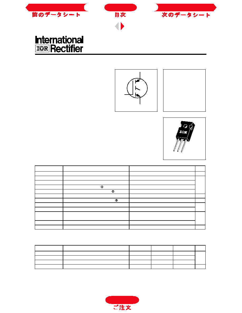
IRGPC40S
Standard Speed IGBT
INSULATED GATE BIPOLAR TRANSISTOR
Features
∑ Switching-loss rating includes all "tail" losses
∑ Optimized for line frequency operation (to 400Hz)
See Fig. 1 for Current vs. Frequency curve
V
CES
= 600V
V
CE(sat)
1.8V
@V
GE
= 15V, I
C
= 31A
E
C
G
n-channel
Description
Insulated Gate Bipolar Transistors (IGBTs) from International Rectifier have
higher usable current densities than comparable bipolar transistors, while at
the same time having simpler gate-drive requirements of the familiar power
MOSFET. They provide substantial benefits to a host of high-voltage, high-
current applications.
Absolute Maximum Ratings
Parameter
Max.
Units
V
CES
Collector-to-Emitter Voltage
600
V
I
C
@ T
C
= 25∞C
Continuous Collector Current
50
I
C
@ T
C
= 100∞C
Continuous Collector Current
31
A
I
CM
Pulsed Collector Current
240
I
LM
Clamped Inductive Load Current
120
V
GE
Gate-to-Emitter Voltage
±20
V
E
ARV
Reverse Voltage Avalanche Energy
15
mJ
P
D
@ T
C
= 25∞C
Maximum Power Dissipation
160
W
P
D
@ T
C
= 100∞C
Maximum Power Dissipation
65
T
J
Operating Junction and
-55 to +150
T
STG
Storage Temperature Range
∞C
Soldering Temperature, for 10 sec.
300 (0.063 in. (1.6mm) from case)
Mounting torque, 6-32 or M3 screw.
10 lbf∑in (1.1N∑m)
Thermal Resistance
TO-247AC
PD - 9.692A
Next Data Sheet
Index
Previous Datasheet
To Order
C-28
IRGPC40S
Parameter
Min. Typ. Max. Units
Conditions
Q
g
Total Gate Charge (turn-on)
--
62
90
I
C
= 31A
Q
ge
Gate - Emitter Charge (turn-on)
--
10
15
nC
V
CC
= 400V
See Fig. 8
Q
gc
Gate - Collector Charge (turn-on)
--
27
40
V
GE
= 15V
t
d(on)
Turn-On Delay Time
--
28
--
T
J
= 25∞C
t
r
Rise Time
--
50
--
ns
I
C
= 31A, V
CC
= 480V
t
d(off)
Turn-Off Delay Time
--
1100 1500
V
GE
= 15V, R
G
= 10
t
f
Fall Time
--
620 1100
Energy losses include "tail"
E
on
Turn-On Switching Loss
--
1.0
--
E
off
Turn-Off Switching Loss
--
12
--
mJ
See Fig. 9, 10, 11, 14
E
ts
Total Switching Loss
--
13
20
t
d(on)
Turn-On Delay Time
--
29
--
T
J
= 150∞C,
t
r
Rise Time
--
53
--
ns
I
C
= 31A, V
CC
= 480V
t
d(off)
Turn-Off Delay Time
--
1600
--
V
GE
= 15V, R
G
= 10
t
f
Fall Time
--
1200
--
Energy losses include "tail"
E
ts
Total Switching Loss
--
22
--
mJ
See Fig. 10, 14
L
E
Internal Emitter Inductance
--
7.5
--
nH
Measured 5mm from package
C
ies
Input Capacitance
--
1600
--
V
GE
= 0V
C
oes
Output Capacitance
--
140
--
pF
V
CC
= 30V
See Fig. 7
C
res
Reverse Transfer Capacitance
--
20
--
= 1.0MHz
Notes:
V
CC
=80%(V
CES
), V
GE
=20V, L=10µH,
R
G
= 10
, ( See fig. 13a )
Repetitive rating; V
GE
=20V, pulse width
limited by max. junction temperature.
( See fig. 13b )
Repetitive rating; pulse width limited
by maximum junction temperature.
Pulse width
80µs; duty factor
0.1%.
Pulse width 5.0µs,
single shot.
Switching Characteristics @ T
J
= 25∞C (unless otherwise specified)
Parameter
Min. Typ. Max. Units
Conditions
V
(BR)CES
Collector-to-Emitter Breakdown Voltage
600
--
--
V
V
GE
= 0V, I
C
= 250µA
V
(BR)ECS
Emitter-to-Collector Breakdown Voltage
20
--
--
V
V
GE
= 0V, I
C
= 1.0A
V
(BR)CES
/
T
J
Temp. Coeff. of Breakdown Voltage
--
0.75
--
V/∞C
V
GE
= 0V, I
C
= 1.0mA
V
CE(on)
Collector-to-Emitter Saturation Voltage
--
1.6
1.8
I
C
= 31A
V
GE
= 15V
--
2.2
--
V
I
C
= 60A
See Fig. 2, 5
--
1.7
--
I
C
= 31A, T
J
= 150∞C
V
GE(th)
Gate Threshold Voltage
3.0
--
5.5
V
CE
= V
GE
, I
C
= 250µA
V
GE(th)
/
T
J
Temp. Coeff. of Threshold Voltage
--
-9.3
-- mV/∞C V
CE
= V
GE
, I
C
= 250µA
g
fe
Forward Transconductance
12
21
--
S
V
CE
= 100V, I
C
= 31A
I
CES
Zero Gate Voltage Collector Current
--
--
250
µA
V
GE
= 0V, V
CE
= 600V
--
--
1000
V
GE
= 0V, V
CE
= 600V, T
J
= 150∞C
I
GES
Gate-to-Emitter Leakage Current
--
--
±100
nA
V
GE
= ±20V
Electrical Characteristics @ T
J
= 25∞C (unless otherwise specified)
Next Data Sheet
Index
Previous Datasheet
To Order
C-29
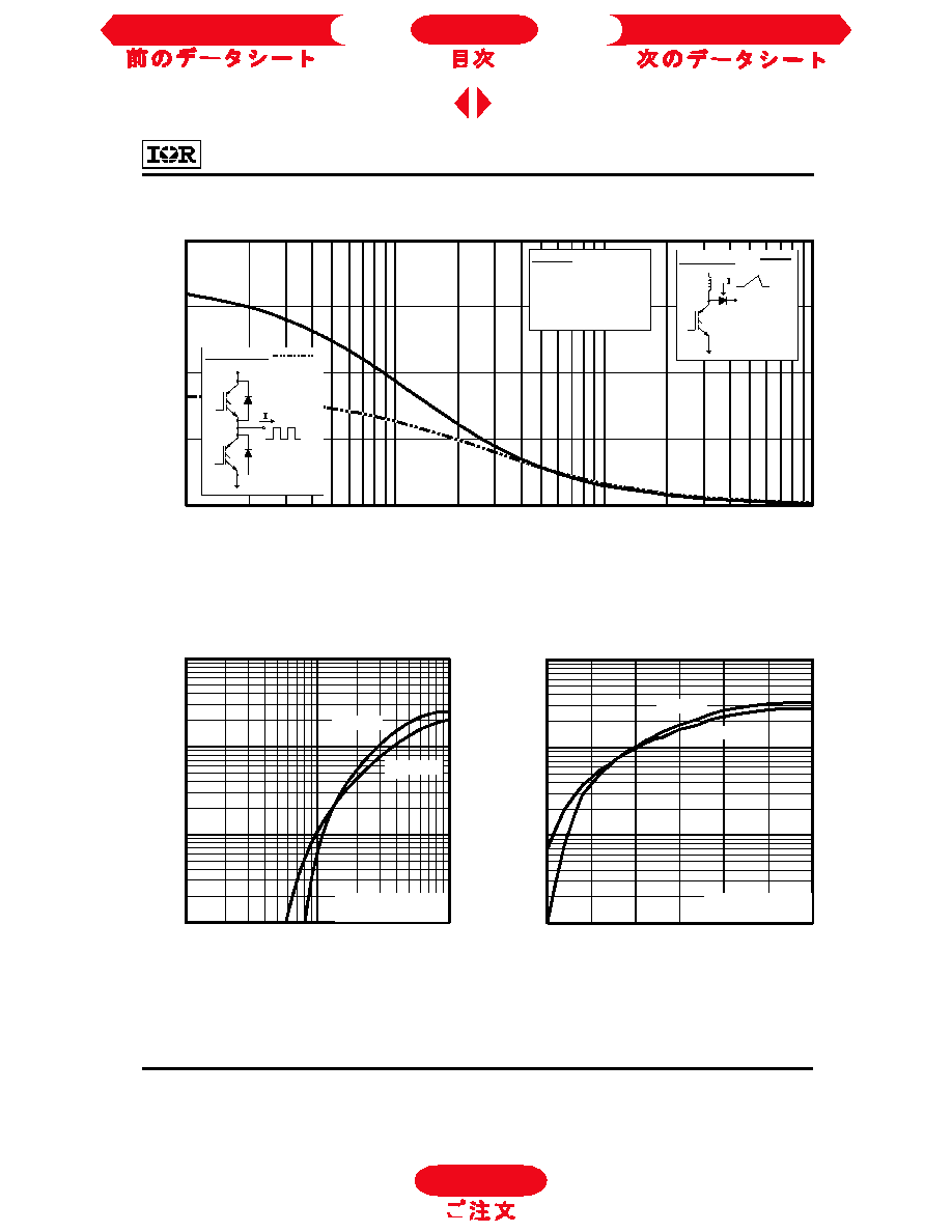
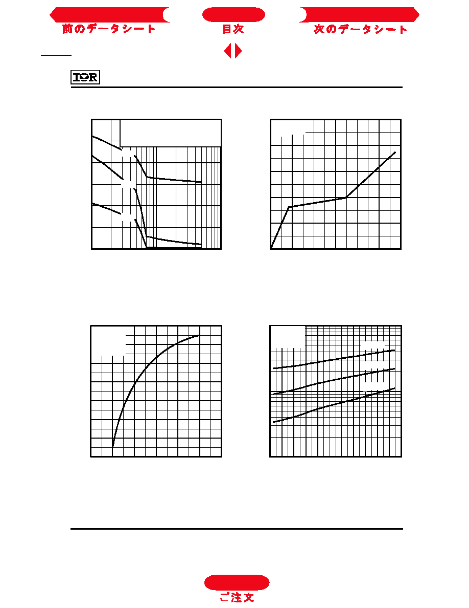
Fig. 1 - Typical Load Current vs. Frequency
(For square wave, I=I
RMS
of fundamental; for triangular wave, I=I
PK
)
Fig. 2 - Typical Output Characteristics
Fig. 3 - Typical Transfer Characteristics
IRGPC40S
0
2 0
4 0
6 0
8 0
0 .1
1
1 0
1 0 0
L
O
A
D
C
U
R
R
E
N
T
(
A
)
f, F re quency (kH z)
6 0% o f ra te d
vo lta ge
Id ea l diodes
S qu a re w a ve :
Tria ng u la r w a v e:
C lam p vo lta g e :
8 0% o f ra te d
F o r bo th:
D u ty c yc le : 5 0 %
T = 1 25 ∞ C
T = 9 0 ∞C
G a te d riv e a s s p e c ifie d
s in k
J
P o w e r D issip a tion = 3 5 W
1
1 0
1 0 0
1 0 0 0
0 .1
1
1 0
C E
C
I
,
C
o
l
l
e
c
t
o
r
-
t
o
-
E
m
i
t
t
e
r
C
u
r
r
e
n
t
(
A
)
V , C o llector-to-E m itter V oltage (V )
T = 15 0∞C
T = 25 ∞C
J
J
V = 15 V
20 µs P U L S E W ID T H
G E
1
1 0
1 0 0
1 0 0 0
5
1 0
1 5
2 0
C
I
,
C
o
l
l
e
c
t
o
r
-
t
o
-
E
m
i
t
t
e
r
C
u
r
r
e
n
t
(
A
)
V , G a te -to -E m itte r V o lta g e (V )
G E
T = 25 ∞C
J
V = 1 00 V
5 µ s P U L S E W ID T H
C C
T = 1 50 ∞C
J
To Order
Next Data Sheet
Index
Previous Datasheet
C-30
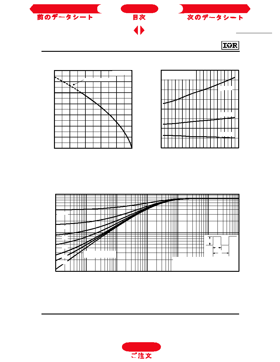
Fig. 5 - Collector-to-Emitter Voltage vs.
Case Temperature
Fig. 4 - Maximum Collector Current vs.
Case Temperature
IRGPC40S
Fig. 6 - Maximum Effective Transient Thermal Impedance, Junction-to-Case
0
1 0
2 0
3 0
4 0
5 0
6 0
7 0
2 5
5 0
7 5
1 0 0
1 2 5
1 5 0
M
a
x
i
m
u
m
D
C
C
o
l
l
e
c
t
o
r
C
u
r
r
e
n
t
(
A
)
T , C ase T em perature (∞C )
C
V = 1 5V
G E
LIMITED BY PACKAGE
1 .0
1 .5
2 .0
2 .5
3 .0
-6 0
-4 0
-2 0
0
2 0
4 0
6 0
8 0
1 0 0 1 2 0 1 4 0 1 6 0
T , C ase T em perature (∞C )
C
C
E
V
,
C
o
l
l
e
c
t
o
r
-
t
o
-
E
m
i
t
t
e
r
V
o
l
t
a
g
e
(
V
)
V = 1 5 V
80 µs P U L S E W ID T H
G E
I = 62 A
I = 31 A
I = 1 6A
C
C
C
0 .0 1
0 .1
1
0 .0 0 0 0 1
0 .0 0 0 1
0 .0 0 1
0 .0 1
0 .1
1
1 0
t , R ectangular P ulse D uration (sec)
1
t
h
J
C
D = 0 .5 0
0.0 1
0.0 2
0 .05
0.1 0
0.2 0
SIN G LE P UL SE
(T H ER M A L R E SP O NS E )
T
h
e
r
m
a
l
R
e
s
p
o
n
s
e
(
Z
)
P
t
2
1
t
D M
N o te s:
1 . D u ty fa c to r D = t / t
2 . P e a k T = P x Z + T
1
2
J
D M
th J C
C
To Order
Next Data Sheet
Index
Previous Datasheet
C-31
IRGPC40S
Fig. 7 - Typical Capacitance vs.
Collector-to-Emitter Voltage
Fig. 8 - Typical Gate Charge vs.
Gate-to-Emitter Voltage
Fig. 9 - Typical Switching Losses vs. Gate
Resistance
Fig. 10 - Typical Switching Losses vs.
Case Temperature
1 3 .2
1 3 .4
1 3 .6
1 3 .8
1 4 .0
1 4 .2
1 4 .4
1 4 .6
0
10
2 0
3 0
40
5 0
6 0
G
T
o
t
a
l
S
w
i
t
c
h
i
n
g
L
o
s
s
e
s
(
m
J
)
R , G ate R es istance ( )
W
V = 4 80 V
V = 15 V
T = 25 ∞C
I = 3 1A
C C
G E
C
C
1
1 0
1 0 0
-6 0
-4 0
-2 0
0
2 0
4 0
6 0
8 0
1 0 0 1 2 0 1 4 0 1 6 0
C
T , C a se T e m p e ra tu re (∞C )
T
o
t
a
l
S
w
i
t
c
h
i
n
g
L
o
s
s
e
s
(
m
J
)
R = 10
V = 1 5V
V = 48 0V
G
GE
CC
I = 6 2A
I = 3 1A
I = 16 A
C
C
C
0
10 0 0
20 0 0
30 0 0
1
1 0
1 0 0
C E
C
,
C
a
p
a
c
i
t
a
n
c
e
(
p
F
)
V , C o llector-to-E m itter V oltage (V )
V = 0V, f = 1MHz
C = C + C , C SHORTED
C = C
C = C + C
GE
ies ge gc ce
res gc
oes ce gc
C
ies
C
res
C
oes
0
4
8
12
16
20
0
1 0
2 0
3 0
40
5 0
6 0
G
E
V
,
G
a
t
e
-
t
o
-
E
m
i
t
t
e
r
V
o
l
t
a
g
e
(
V
)
Q , T otal G ate C harge (nC )
g
V = 40 0 V
I = 3 1A
C E
C
Revision 0
To Order
Next Data Sheet
Index
Previous Datasheet