 | ÐлекÑÑоннÑй компоненÑ: IRGPH50M | СкаÑаÑÑ:  PDF PDF  ZIP ZIP |
Äîêóìåíòàöèÿ è îïèñàíèÿ www.docs.chipfind.ru
C-471
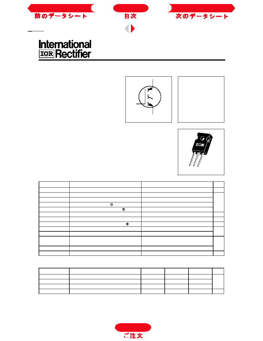
IRGPH50M
Short Circuit Rated
Fast IGBT
INSULATED GATE BIPOLAR TRANSISTOR
Parameter
Min.
Typ.
Max.
Units
R
JC
Junction-to-Case
--
--
0.64
R
CS
Case-to-Sink, flat, greased surface
--
0.24
--
°C/W
R
JA
Junction-to-Ambient, typical socket mount
--
--
40
Wt
Weight
--
6 (0.21)
--
g (oz)
Features
· Short circuit rated - 10µs @ 125°C, V
GE
= 15V
· Switching-loss rating includes all "tail" losses
· Optimized for medium operating frequency (1 to
10kHz) See Fig. 1 for Current vs. Frequency
V
CES
= 1200V
V
CE(sat)
2.9V
@V
GE
= 15V, I
C
= 23A
E
C
G
n-channel
Absolute Maximum Ratings
Parameter
Max.
Units
V
CES
Collector-to-Emitter Voltage
1200
V
I
C
@ T
C
= 25°C
Continuous Collector Current
42
I
C
@ T
C
= 100°C
Continuous Collector Current
23
A
I
CM
Pulsed Collector Current
84
I
LM
Clamped Inductive Load Current
84
t
sc
Short Circuit Withstand Time
10
µs
V
GE
Gate-to-Emitter Voltage
±20
V
E
ARV
Reverse Voltage Avalanche Energy
20
mJ
P
D
@ T
C
= 25°C
Maximum Power Dissipation
200
W
P
D
@ T
C
= 100°C
Maximum Power Dissipation
78
T
J
Operating Junction and
-55 to +150
T
STG
Storage Temperature Range
°C
Soldering Temperature, for 10 sec.
300 (0.063 in. (1.6mm) from case)
Mounting torque, 6-32 or M3 screw.
10 lbf·in (1.1N·m)
TO-247AC
PD - 9.1030
Thermal Resistance
Insulated Gate Bipolar Transistors (IGBTs) from International Rectifier have
higher usable current densities than comparable bipolar transistors, while at
the same time having simpler gate-drive requirements of the familiar power
MOSFET. They provide substantial benefits to a host of high-voltage, high-
current applications.
These new short circuit rated devices are especially suited for motor control
and other applications requiring short circuit withstand capability.
Description
curve
Revision 1
Next Data Sheet
Index
Previous Datasheet
To Order
C-472
IRGPH50M
Notes:
Repetitive rating; V
GE
=20V, pulse width
limited by max. junction temperature.
( See fig. 13b )
Repetitive rating; pulse width limited
by maximum junction temperature.
Pulse width
80µs; duty factor
0.1%.
Pulse width 5.0µs,
single shot.
Switching Characteristics @ T
J
= 25°C (unless otherwise specified)
Parameter
Min. Typ. Max. Units
Conditions
Q
g
Total Gate Charge (turn-on)
--
89
130
I
C
= 23A
Q
ge
Gate - Emitter Charge (turn-on)
--
22
33
nC
V
CC
= 400V
See Fig. 8
Q
gc
Gate - Collector Charge (turn-on)
--
26
39
V
GE
= 15V
t
d(on)
Turn-On Delay Time
--
42
--
T
J
= 25°C
t
r
Rise Time
--
32
--
ns
I
C
= 23A, V
CC
= 960V
t
d(off)
Turn-Off Delay Time
--
280
820
V
GE
= 15V, R
G
= 5.0
t
f
Fall Time
--
190
410
Energy losses include "tail"
E
on
Turn-On Switching Loss
--
1.6
--
E
off
Turn-Off Switching Loss
--
3.3
--
mJ
See Fig. 9, 10, 11, 14
E
ts
Total Switching Loss
--
4.9
11
t
sc
Short Circuit Withstand Time
10
--
--
µs
V
CC
= 720V, T
J
= 125°C
V
GE
= 15V, R
G
= 5.0
, V
CPK
< 1000V
t
d(on)
Turn-On Delay Time
--
32
--
T
J
= 150°C,
t
r
Rise Time
--
21
--
ns
I
C
= 23A, V
CC
= 960V
t
d(off)
Turn-Off Delay Time
--
490
--
V
GE
= 15V, R
G
= 5.0
t
f
Fall Time
--
440
--
Energy losses include "tail"
E
ts
Total Switching Loss
--
10
--
mJ
See Fig. 10, 14
L
E
Internal Emitter Inductance
--
13
--
nH
Measured 5mm from package
C
ies
Input Capacitance
--
1900
--
V
GE
= 0V
C
oes
Output Capacitance
--
140
--
pF
V
CC
= 30V
See Fig. 7
C
res
Reverse Transfer Capacitance
--
24
--
= 1.0MHz
Parameter
Min. Typ. Max. Units
Conditions
V
(BR)CES
Collector-to-Emitter Breakdown Voltage
1200
--
--
V
V
GE
= 0V, I
C
= 250µA
V
(BR)ECS
Emitter-to-Collector Breakdown Voltage
20
--
--
V
V
GE
= 0V, I
C
= 1.0A
V
(BR)CES
/
T
J
Temp. Coeff. of Breakdown Voltage
--
1.1
--
V/°C
V
GE
= 0V, I
C
= 1.0mA
V
CE(on)
Collector-to-Emitter Saturation Voltage
--
2.3
2.9
I
C
= 23A
V
GE
= 15V
--
3.0
--
V
I
C
= 42A
See Fig. 2, 5
--
2.8
--
I
C
= 23A, T
J
= 150°C
V
GE(th)
Gate Threshold Voltage
3.0
--
5.5
V
CE
= V
GE
, I
C
= 250µA
V
GE(th)
/
T
J
Temp. Coeff. of Threshold Voltage
--
-13
-- mV/°C V
CE
= V
GE
, I
C
= 250µA
g
fe
Forward Transconductance
11
15
--
S
V
CE
= 100V, I
C
= 23A
I
CES
Zero Gate Voltage Collector Current
--
--
250
µA
V
GE
= 0V, V
CE
= 1200V
--
--
2000
V
GE
= 0V, V
CE
= 1200V, T
J
= 150°C
I
GES
Gate-to-Emitter Leakage Current
--
--
±100
nA
V
GE
= ±20V
Electrical Characteristics @ T
J
= 25°C (unless otherwise specified)
V
CC
=80%(V
CES
), V
GE
=20V, L=10µH,
R
G
= 5.0
, ( See fig. 13a )
Next Data Sheet
Index
Previous Datasheet
To Order
C-473
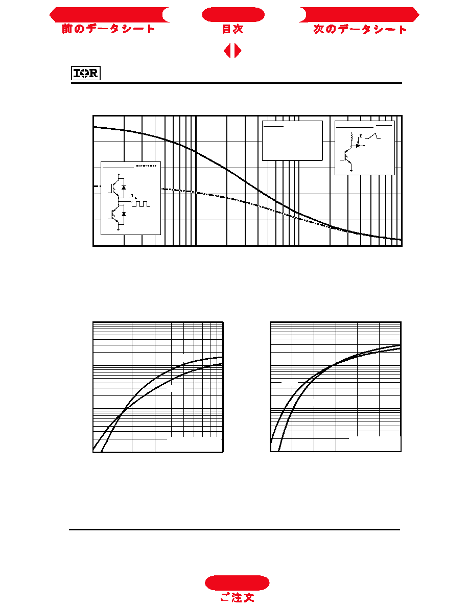
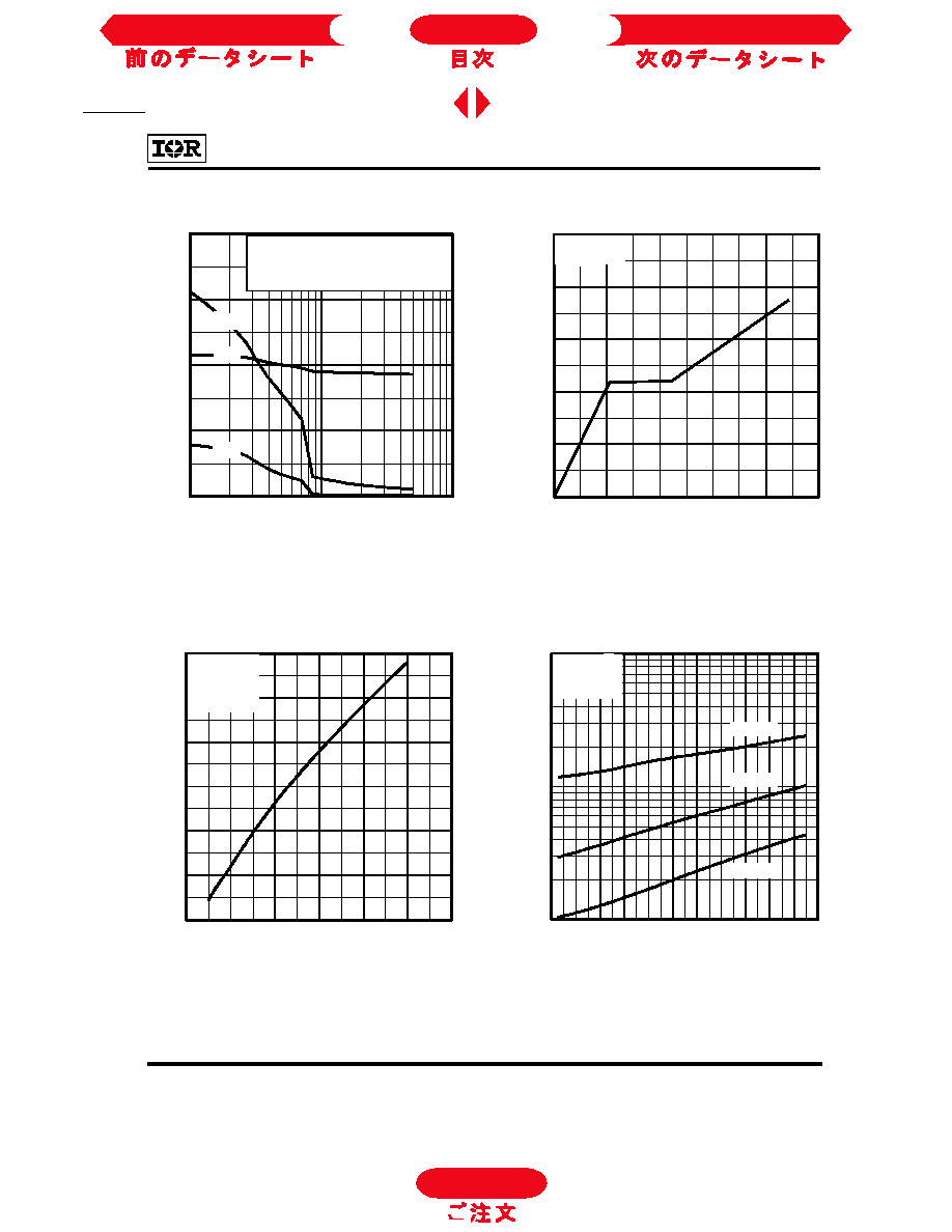
Fig. 1 - Typical Load Current vs. Frequency
(For square wave, I=I
RMS
of fundamental; for triangular wave, I=I
PK
)
Fig. 2 - Typical Output Characteristics
Fig. 3 - Typical Transfer Characteristics
IRGPH50M
0
1 0
2 0
3 0
4 0
5 0
0 .1
1
1 0
1 0 0
L
O
A
D
C
U
R
R
E
N
T
(
A
)
f, F re quency (kH z)
60 % of ra ted
vo lta g e
Ideal d iod es
S qu a re w ave :
F or b oth :
D u ty c y cle : 5 0 %
T = 1 2 5 °C
T = 9 0 ° C
G a te d riv e as sp e c ifie d
sin k
J
P o w e r D is sip a tio n = 4 0W
Tria n g u la r w a ve :
C la mp vo lta g e:
80 % o f ra te d
1
1 0
1 0 0
1 0 0 0
1
1 0
C E
C
I
,
C
o
l
l
e
c
t
o
r
-
t
o
-
E
m
i
t
t
e
r
C
u
r
r
e
n
t
(
A
)
1 50 °C
25 °C
V , C ollector-to-E m itter V oltage (V )
V = 15 V
20 µ s P U L S E W ID T H
GE
1
1 0
1 0 0
1 0 0 0
5
1 0
1 5
2 0
C
I
,
C
o
l
l
e
c
t
o
r
-
t
o
-
E
m
i
t
t
e
r
C
u
r
r
e
n
t
(
A
)
1 5 0°C
2 5°C
V , G a te -to -E m itte r V o lta g e (V)
V = 1 0 0V
5 µ s P U L S E W ID T H
C C
G E
To Order
Next Data Sheet
Index
Previous Datasheet
C-474
Fig. 5 - Collector-to-Emitter Voltage vs.
Case Temperature
Fig. 4 - Maximum Collector Current vs.
Case Temperature
IRGPH50M
Fig. 6 - Maximum Effective Transient Thermal Impedance, Junction-to-Case
0
1 0
2 0
3 0
4 0
5 0
2 5
5 0
7 5
1 0 0
1 2 5
1 5 0
M
a
x
i
m
u
m
D
C
C
o
l
l
e
c
t
o
r
C
u
r
r
e
n
t
(
A
)
T , C ase T em perature (°C )
C
V = 1 5V
GE
1 .0
1 .5
2 .0
2 .5
3 .0
3 .5
4 .0
4 .5
5 .0
5 .5
6 .0
-6 0
-4 0
-2 0
0
2 0
4 0
6 0
8 0
1 0 0 1 2 0 1 4 0 1 6 0
T , C ase T em p erature (°C )
C
C
E
V
,
C
o
l
l
e
c
t
o
r
-
t
o
-
E
m
i
t
t
e
r
V
o
l
t
a
g
e
(
V
)
I = 4 6A
I = 2 3A
I = 12A
C
C
C
V = 1 5V
8 0 µs P U L S E W ID T H
G E
0 .0 1
0 .1
1
0 .0 0 0 0 1
0 .0 0 0 1
0 .0 0 1
0 .0 1
0 .1
1
1 0
t , R e c ta n gu lar P u ls e D u ra tion (s e c )
1
t
h
J
C
D = 0 .5 0
0 .0 1
0 .0 2
0 .0 5
0 .1 0
0 .2 0
S IN G L E P U LS E
(T H E R M A L R E S P O N S E )
T
h
e
r
m
a
l
R
e
s
p
o
n
s
e
(
Z
)
P
t
2
1
t
D M
N ote s :
1 . D u ty fa ct or D = t / t
2 . P e a k T = P x Z + T
1
2
J
D M
th J C
C
To Order
Next Data Sheet
Index
Previous Datasheet
C-475
IRGPH50M
Fig. 7 - Typical Capacitance vs.
Collector-to-Emitter Voltage
Fig. 8 - Typical Gate Charge vs.
Gate-to-Emitter Voltage
Fig. 9 - Typical Switching Losses vs. Gate
Resistance
Fig. 10 - Typical Switching Losses vs.
Case Temperature
0
1 0 0 0
2 0 0 0
3 0 0 0
4 0 0 0
1
10
1 0 0
C E
C
,
C
a
p
a
c
i
t
a
n
c
e
(
p
F
)
V , C ollector-to-E m itter V oltage (V )
C res
C oes
C ies
V = 0 V , f = 1 M H z
C = C + C , C S H O R T E D
C = C
C = C + C
G E
ie s g e g c c e
re s g c
o e s c e g c
0
4
8
12
16
20
0
20
4 0
60
8 0
1 0 0
G
E
V
,
G
a
t
e
-
t
o
-
E
m
i
t
t
e
r
V
o
l
t
a
g
e
(
V
)
Q , T otal G a te C ha rge (nC )
G
V = 4 00 V
I = 2 3 A
CE
C
4.8
5.0
5.2
5.4
5.6
5.8
6.0
0
10
20
30
40
50
60
G
T
o
t
a
l
S
w
i
t
c
h
i
n
g
L
o
s
s
e
s
(
m
J
)
R , Gate Resistance (
)
A
V = 960V
V = 15V
T = 25°C
I = 23A
CC
GE
C
C
1
1 0
1 0 0
-6 0
-4 0
-2 0
0
2 0
4 0
6 0
8 0
1 0 0 1 2 0 1 4 0 1 6 0
T , C a se T em perature (°C )
C
T
o
t
a
l
S
w
i
t
c
h
i
n
g
L
o
s
s
e
s
(
m
J
)
R = 5
V = 1 5V
V = 9 60 V
I = 46 A
I = 23 A
I = 11 A
C
C
C
G
G E
C C
To Order
Next Data Sheet
Index
Previous Datasheet