 | –≠–ª–µ–∫—Ç—Ä–æ–Ω–Ω—ã–π –∫–æ–º–ø–æ–Ω–µ–Ω—Ç: IRKT136 | –°–∫–∞—á–∞—Ç—å:  PDF PDF  ZIP ZIP |
135 A
140 A
160 A
Bulletin I27117 rev. C 03/02
1
SERIES
IRK.136, .142, .162
NEW INT-A-pak Power Modules
I
T(AV)
135
140
160
A
@ T
C
85
85
85
∞C
I
T(RMS)
300
310
355
A
I
TSM
@ 50Hz
3200
4500
4870
A
@ 60Hz
3360
4712
5100
A
I
2
t @ 50Hz
51.5
102
119
KA
2
s
@ 60Hz
47
92.5
108
KA
2
s
I
2
t
515.5
1013
1190
KA
2
s
V
RRM
400 to 1600
V
T
J
range
- 40 to 125
∞C
Major Ratings and Characteristics
Features
High Voltage
Electrically Isolated by DBC Ceramic ( Al
2
O
3
)
3500 V
RMS
Isolating Voltage
Industrial Standard Package
High Surge Capability
Glass Passivated Chips
Modules uses High Voltage Power thyristor/diodes
in three Basic Configurations
Simple Mounting
UL E78996 approved
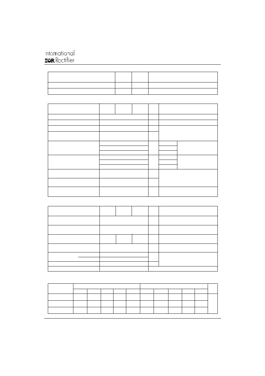
Parameters IRK.136.. IRK.142.. IRK.162.. Units
THYRISTOR/DIODE and
THYRISTOR/THYRISTOR
Applications
DC Motor Control and Drives
Battery Charges
Welders
Power Converters
Lighting Control
Heat and Temperature Control
CASE STYLE NEW INT-A-PAK
www.irf.com

IRK.136, .142, .162 Series
2
Bulletin I27117 rev. C 03/02
www.irf.com
Type number
Voltage
V
RRM
/V
DRM
, Maximum repetitive V
RSM
/V
DSM
, Maximum non-repetitive
I
RRM /
I
DRM
Code
peak reverse voltage
peak reverse voltage
@ 125∞C
V
V
m A
IRK.136
04
400
500
50
IRK.142
08
800
900
IRK.162
12
1200
1300
14
1400
1500
16
1600
1700
I
T(AV)
Max. average on-state current
135
140
160
A
180∞ conduction, half sine wave
@ Case temperature
85
85
85
∞C
I
T(RMS)
Max. RMS on-state current
300
310
355
A
as AC switch
I
TSM
Maximum peak, one-cycle
3200
4500
4870
A
t = 10ms No voltage
on-state, non-repetitive
3360
4712
5100
t = 8.3ms reapplied
surge current
2700
3785
4100
t = 10ms 100% V
RRM
2800
3963
4300
t = 8.3ms reapplied
Sine half wave,
I
2
t
Maximum I
2
t for fusing
51.5
102
119
KA
2
s
t = 10ms No voltage
Initial T
J
= T
J
max.
47
92.5
108
t = 8.3ms reapplied
36.5
71.6
84
t = 10ms 100% V
RRM
33.3
65.4
76.7
t = 8.3ms reapplied
I
2
t
Maximum I
2
t for fusing
515.5
1013
1190
KA
2
s t = 0.1 to 10ms, no voltage reapplied
V
T(TO)1
Low level value of threshold
0.86
0.83
0.8
V
(16.7% x
x I
T(AV)
< I <
x I
T(AV)
), @ T
J
max.
voltage
V
T(TO)2
High level value of threshold
1.05
1
0.98
(I >
x I
T(AV)
), @ T
J
max.
voltage
r
t1
Low level value on-state
2.02
1.78
1.67
m
(16.7% x
x I
T(AV)
< I <
x I
T(AV)
), @ T
J
max.
slope resistance
r
t2
High level value on-state
1.65
1.43
1.38
(I >
x I
T(AV)
), @ T
J
max.
slope resistance
V
TM
Maximum forward voltage drop
1.57
1.55
1.54
V
I
TM
=
x I
T(AV)
, T
J
= 25∞C, 180∞conduction
I
H
Maximum holding current
200
mA
Anode supply = 6V initial I
T
= 30A, T
J
= 25∞C
I
L
Maximum latching current
400
mA
Anode supply = 6V resistive load = 1
Gate pulse: 10V, 100µs, T
J
= 25∞C
t
gd
Typical delay time
1
T
J
= 25
o
C
Gate Current=1A dIg/
dt
=1A/µs
t
gr
Typical rise time
2
µs
T
J
= 25
o
C
Vd=0,67% V
DRM
t
q
Typical turn-off time
50 - 200
I
TM
= 300 A; -dI/dt = 15 A/µs; T
J
= T
J
max
V
r
= 50 V; dV/dt = 20 V/µs; Gate 0 V, 100
Parameter
IRK.136
IRK.142
IRK.162
Units Conditions
Forward Conduction
Switching
Electrical Specifications
Voltage Ratings
IRK.136, .142, .162 Series
3
Bulletin I27117 rev. C 03/02
www.irf.com
Thermal and Mechanical Specifications
T
J
Max. junction operating
-40 to 125
∞C
temperature range
T
stg
Max. storage temperature
-40 to 150
∞C
range
R
thJC
Max. thermal resistance,
0.18
0.18
0.16
K/W
DC operation, per junction
junction to case
R
thCS
Max. thermal resistance,
0.05
K/W
Mounting surface smooth, flat and greased
case to heatsink
Per module
T
Mounting
IAP to heatsink
4 to 6
Nm
torque ± 10% busbar to IAP
4 to 6
wt
Approximate weight
200 (7.1)
g(oz)
Case Style
New Int-A-Pak
A mounting compound is recommended and
the torque should be rechecked after a period
of 3 hours to allow for the spread of the
compound. Lubricated threads.
Triggering
P
GM
Max. peak gate power
12
W
tp
5ms, T
J
= T
J
max.
P
G(AV)
Max. average gate power
3
W
f=50Hz, T
J
= T
J
max.
I
GM
Max. peak gate current
3
A
tp
5ms, T
J
= T
J
max.
-V
GT
Max. peak negative
10
V
gate voltage
V
GT
Max. required DC gate
4
V
T
J
= - 40∞C
Anode supply = 6V, resistive
voltage to trigger
2.5
T
J
= 25∞C
load; Ra = 1
1.7
T
J
= T
J
max.
I
GT
Max. required DC gate
270
T
J
= - 40∞C
Anode supply = 6V, resistive
current to trigger
150
mA
T
J
= 25∞C
load; Ra = 1
80
T
J
= T
J
max.
V
GD
Max. gate voltage
0.3
V
@ T
J
= T
J
max., rated V
DRM
applied
that will not trigger
I
GD
Max. gate current
10
mA
that will not trigger
di/
dt
Max. rate of rise of
300
A/µs
@ T
J
= T
J
max., I
TM
= 400A
rated V
DRM
applied
turned-on current
Sinusoidal conduction @ T
J
max.
Rectangular conduction @ T
J
max.
Devices
Units
180
o
120
o
90
o
60
o
30
o
180
o
120
o
90
o
60
o
30
o
IRK.136
0.007
0.01
0.013
0.0155
0.017
0.009
0.012
0.014
0.015
0.017
IRK.142
0.0019
0.0019
0.0020
0.0020
0.0021
0.0018
0.0022
0.0023
0.0023
0.0020 K/W
IRK.162
0.0030
0.0031
0.0032
0.0033
0.0034
0.0029
0.0036
0.0039
0.0041
0.0040
R Conduction (per Junction)
(The following table shows the increment of thermal resistance R
thJC
when devices operate at different conduction angles than DC)
Parameter
IRK.136
IRK.142
IRK.162
Units Conditions
Parameter
IRK.136
IRK.142
IRK.162
Units Conditions
Blocking
I
RRM
Maximum peak reverse and
50
mA
T
J
= 125
o
C
I
DRM
off-state leakage current
V
INS
RMS isolation voltage
3500
V
50Hz, circuit to base, all terminals shorted, t = 1s
dV/dt critical rate of rise of off-state voltage
1000
V/µs
T
J
= T
J
max., exponential to 67% rated V
DRM
IRK.136, .142, .162 Series
4
Bulletin I27117 rev. C 03/02
www.irf.com
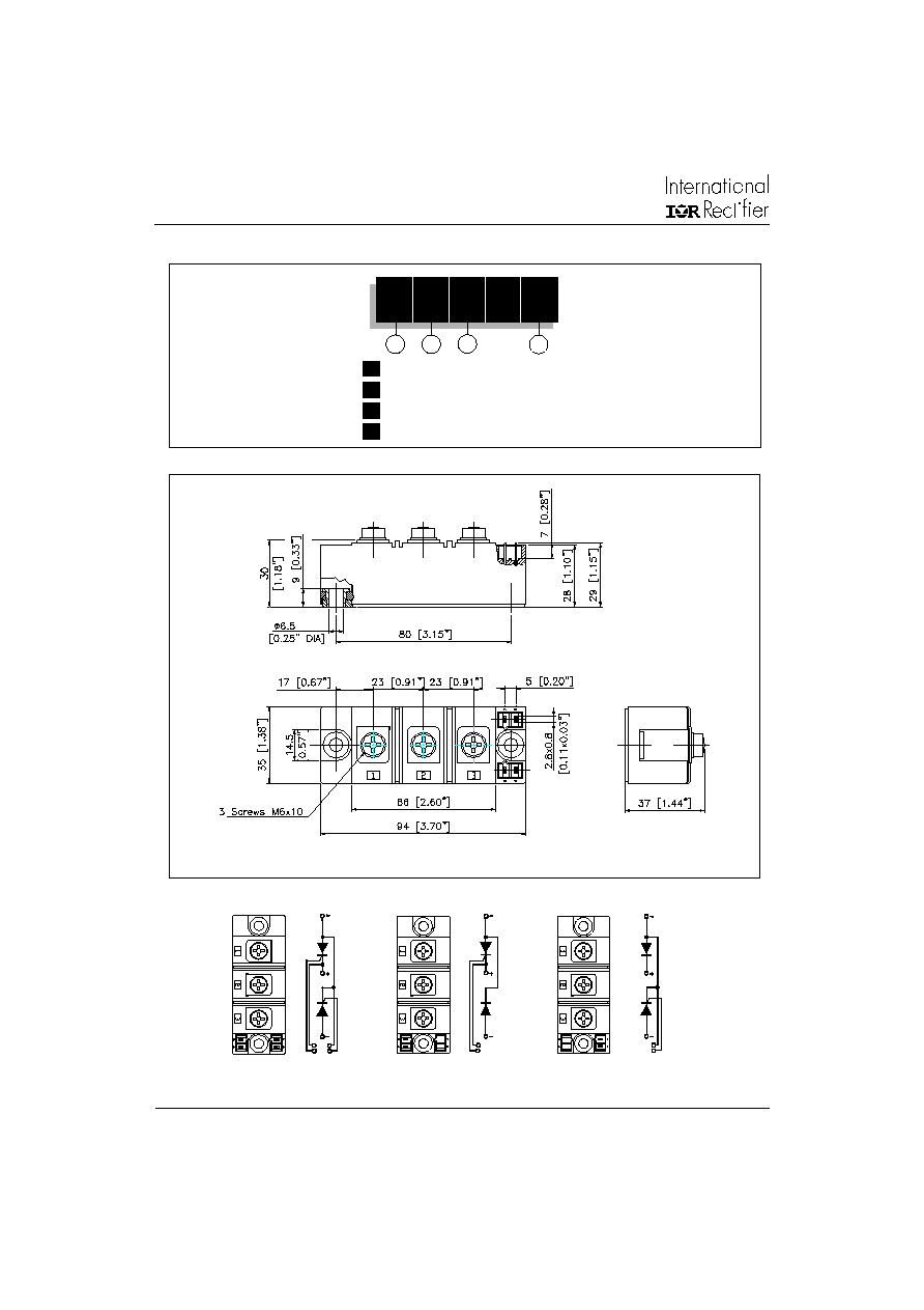
Outline Table
1
2
3
1
-
Module Type
2
-
Circuit Configuration
3
-
Current Rating: I
T(AV)
4
-
Voltage Code: Code x 100 = V
RRM
4
Device Code
Ordering Information Table
IRK
T
162
/
16
Dimensions are in millimeters and [inches]
NOTE: To order the Optional Hardware see Bulletin I27900
5
4
3
6
7
1
2
1
2
3
4
5
2
1
3
7
6
IRKT
IRKH
IRKL
IRK.136, .142, .162 Series
5
Bulletin I27117 rev. C 03/02
www.irf.com
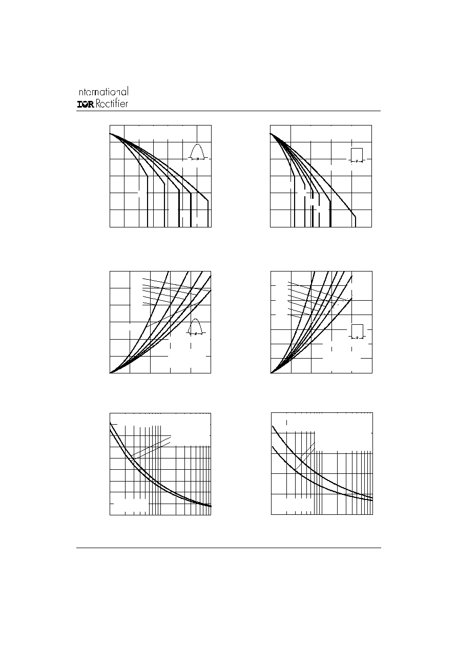
Fig.5 - Maximum Non-Repetitive Surge Current
Fig. 6 - Maximum Non-Repetitive Surge Current
Fig. 1 - Current Ratings Characteristics
Fig. 4 - On-State Power Loss Characteristics
Fig. 3 - On-State Power Loss Characteristics
Fig. 2 - Current Ratings Characteristics
7 0
8 0
9 0
10 0
11 0
12 0
13 0
0
5 0
1 0 0
15 0
2 00
25 0
D C
3 0
6 0
9 0
1 2 0
1 8 0
A ve rag e O n -state C urre n t (A )
M
a
x
i
m
u
m A
l
l
o
w
a
b
l
e
C
a
s
e
T
e
mp
e
r
a
t
u
r
e
(
C
)
C o n d u c tio n P e r io d
IRK .1 3 6 .. Se ries
R (D C ) = 0 .1 8 K/W
thJ C
0
5 0
1 0 0
1 5 0
2 0 0
2 5 0
3 0 0
0
3 0
6 0
9 0
12 0
15 0
RM S Lim it
C o nd uc tio n A ng le
M
a
x
i
m
u
m
A
v
er
a
g
e O
n
-
s
t
a
t
e
P
o
w
e
r
L
o
s
s
(
W
)
A ve rag e O n -state C urre n t (A)
180
120
90
60
30
IRK .136.. Se ries
Per Junctio n
T = 125 C
J
0
5 0
1 0 0
1 5 0
2 0 0
2 5 0
3 0 0
3 5 0
0
50
1 00
1 50
2 00
2 50
RM S Lim it
C o n d uc tio n P e riod
M
a
x
i
m
u
m
Av
er
a
g
e O
n
-
s
t
a
t
e
P
o
w
e
r
L
o
s
s
(
W
)
A ve ra g e O n -sta te C urre n t (A)
D C
180
120
90
60
30
IRK .136.. Se ries
Per Junctio n
T = 12 5 C
J
12 0 0
14 0 0
16 0 0
18 0 0
20 0 0
22 0 0
24 0 0
26 0 0
28 0 0
30 0 0
1
1 0
10 0
N um b er O f Eq ua l A m p litud e H a lf C yc le C urre nt P ulses (N )
A t A ny R a te d Lo a d C o nd itio n A n d W ith
R ated V A p plied Follo w ing Surge .
RRM
P
e
a
k
H
a
l
f
S
i
n
e
W
a
v
e
O
n
-
s
ta
t
e
C
u
r
r
e
n
t
(
A
)
In itial T = 125 C
@ 60 Hz 0.00 83 s
@ 50 Hz 0.01 00 s
J
IRK.136.. Se rie s
Per Junc tion
10 0 0
15 0 0
20 0 0
25 0 0
30 0 0
35 0 0
0 .0 1
0.1
1
P
e
ak
Ha
l
f
S
i
n
e
W
a
v
e
O
n
-
s
t
a
te
C
u
r
r
e
n
t
(
A
)
Pulse Tra in D ura tion (s)
Maxim um No n Repetitive Surge Curre nt
O f Co nd uctio n M ay Not Be M ainta ined .
IRK.1 36.. Se ries
Pe r Ju nctio n
In itial T = 125 C
N o V oltag e Re ap plie d
Ra te d V Re ap plie d
J
R R M
V ers us Pulse Train D ura tio n. C ontrol
7 0
8 0
9 0
10 0
11 0
12 0
13 0
0
2 0
4 0
6 0
8 0
10 0
12 0
14 0
30
60
90
120
180
M
a
x
i
mu
m A
l
l
o
w
a
b
l
e
C
a
s
e
T
e
m
p
e
r
a
t
u
r
e
(
C
)
C o nd uctio n A ng le
A ve rag e Forw ard C urre n t (A )
IRK.136.. Series
R (D C ) = 0.18 K/W
thJ C